Note: Descriptions are shown in the official language in which they were submitted.
CA 02577162 2007-02-14
WO 2006/026621 PCT/US2005/030852
1
MOLYBDENUM SPUTTERING TARGETS
TECHNICAL FIELD OF THE INVENTION
The present invention relates to forms of molybdenum, their use as
sputtering targets and method of their manufacture.
BACKGROUND OF THE INVENTION
The sputtering technique is a film-forming technique with which a plasma
is utilized to generate ions striking a sputtering target so as to result in
atoms of
the sputtering target depositing on a substrate as a film. The sputtering
technique
is particularly used to produce a metallic layer in various manufacturing
processes
used in the semiconductor and the photoelectric industries. The properties of
films formed during sputtering is related to the properties of the sputtering
target
itself, such as the size of the respective crystal grain and the formation of
secondary phase with distribution characteristics.
Various sputtering techniques are used in order to effect the deposition of a
film over the surface of a substrate. Deposited metal films, such as metal
films on
a flat panel display device, can be formed by a magnetron sputtering apparatus
or
other sputtering techniques. The magnetron sputtering apparatus induces plasma
ions of a gas to bombard a target, causing surface atoms of the target
material to
be ejected therefrom and to be deposited as a film or layer on the surface of
a
substrate. Conventionally, a sputtering source in the form of a planar disc or
rectangle is used as the target, and ejected atoms travel along a line-of-
sight
trajectory to deposit on top of a wafer whose deposition face is parallel to
the
erosion face of the target.
However, a tubular-shaped sputtering target can also be used. In this case,
the plasma is external and the atoms are sputtered from the exterior of the
tube.
The flat substrate is slowly passed over the target. Typically, its motion is
horizontal, and in a direction at a right angle to the target axis, which is
also
horizontal. Thus the substrate can be gradually coated as it passes over the
target.
In many cases, sputtering targets, particularly those containing
molybdenum, have a wrought microstructure with non-uniform grain texture,
CA 02577162 2007-02-14
WO 2006/026621 PCT/US2005/030852
2
which may change from one sputtering target to the next. These "non-
uniformities" lead to non-uniform films being deposited onto substrates and
devices, particularly flat panel displays that do not operate optimally.
In other cases, molybdenum-based sputtering targets are manufactured
using a conventional thermomechanical working step. Unfortunately, this
methodology generally induces heterogeneity of grain size and texture. The
heterogeneity in the sputtering targets typically leads to sputtered films
that do not
possess the uniformity desired in most semiconductor and photoelectric
applications.
In some applications, large plates of pure molybdenum are required as
sputtering targets. In such cases, the production of large plates is
accomplished
through the machining and assembly of multiple plates, often referred to as
segmented plates. The preparation of segmented plates requires an increased
amount of machining and assembly cost compared to the production of a single
plate ingot. Additionally, the assembly of different plates creates
variability in the
large segmented plate, which can cause unacceptable variability in films
formed
by sputtering the large plate target.
Therefore, there is a need in the art for molybdenum sputtering targets that
overcome the deficiencies of the prior art and have a fine grain size and
uniform
grain texture.
SUMMARY OF THE INVENTION
The present invention is directed to molybdenum, sputtering targets
characterized as having no or minimal texture banding or through thickness
gradient. The molybdenum sputtering targets having a fine, uniform grain size
as
well as uniform texture, have high purity and can be micro-alloyed to improved
performance.
The present invention is additionally directed to a tubular-shaped sputtering
target
formed by:
A) placing molybdenum powder in a mold and pressing the powder at a
pressure of from 200 to 250 MPa and sintering the pressed piece at a
temperature of from 1780 to 2175 C to form a billet;
CA 02577162 2007-02-14
WO 2006/026621 PCT/US2005/030852
3
B) removing the center of the billet to form a tubular billet having an inner
diameter IDi and an outer diameter ODI;
C) working the tubular billet to form a worked billet having an inner diameter
ID and an outer diameter ODf such that the ratio of ODi to ODf is at least
3:1; and
D) heat treating the tubular billet at a temperature of from 815 to 1375 C.
The present invention is also directed to a tubular-shaped sputtering target
containing molybdenum having a uniform texture, which features particularly a
110 orientation parallel to the longitudinal direction and a 111 orientation
relative
to the radial direction.
The present invention is additionally directed to a method of making a
tubular sputtering target that includes:
A) placing molybdenum powder in a mold and pressing the powder at a
pressure of from 200 to 250 MPa and sintering the pressed piece at a
temperature of from 1780 to 2175 C to form a billet;
B) removing the center of the billet to form a tubular billet having an inner
diameter IDi and an outer diameter ODI;
C) working the tubular billet to form a worked billet having an inner diameter
ID and an outer diameter ODf such that the ratio of OD, to ODf is at least
3 :1; and
D) heat treating the tubular billet at a temperature of from 815 to 1375 C.
Embodiments of the present invention are directed to a disc-shaped
sputtering target formed by:
I) placing molybdenum powder in a mold and pressing the powder at
a pressure of from 200 to 250 MPa and sintering the pressed piece
at a temperature of from 1780 to 2175 C to form a billet having a
diameter of D ;
II) extruding the billet to form an extruded billet having a diameter of
D2 such that the ratio of D. to D2 is from 3:1 to 5:1;
III) applying a first heat treatment to the extruded billet at a
temperature of from 900 to 1300 C;
CA 02577162 2007-02-14
WO 2006/026621 PCT/US2005/030852
4
IV) upset forging the extruded billet at a temperature of from 870 to
1200 C to form a forged billet having a diameter Df such that the
ratio of Df to D2 is from 1.5:1 to 3:1; and
V) applying a second heat treatment to the forged billet at a
temperature of from 1200 to 1400 C.
Embodiments of the invention are also directed to a disc-shaped sputtering
target containing molybdenum having a uniform grain and texture.
Other embodiments of the invention are directed to large molybdenum
plates having a non-segmented construction, weighing at least 300 kg, and
containing at least 99% by weight of molybdenum.
Additional embodiments of the invention are directed to a process for
preparing the above-described plates, which includes the steps of:
i) pouring powder into a sheet bar mold;
ii) consolidating the powder by cold isostatic pressing (C.I.P.) at a
pressures
of from 100 to 250 MPa (15 to 36 ksi) to form a sheet bar;
iii) sintering the sheet bar at a temperature of at least 1600 C to form an
ingot
having a density of at least 90% of the theoretical density;
iv) preheating the ingot at a temperature of from 1100 to 1450 C;
v) hot rolling the ingot at a temperature of from 1050 to 1400 C to effect a
reduction in the thickness and an increase in the length of the ingot; and
vi) heat treating the rolled ingot at a temperature of from 850 to 950 C.
The present invention is further directed to sputtering targets and sintering
tiles that include the above-described molybdenum plate.
The present invention is additionally directed to a method of sputtering
that includes subjecting any of the above-described sputtering targets to
sputtering
conditions and thereby sputtering the target.
The present invention is further directed to a method of sputtering that
includes subjecting the above-described sputtering target to sputtering
conditions
and thereby sputtering the target.
The present invention is further directed to a method for making a thin
film including the steps of:
(a) sputtering the above-described sputtering target;
CA 02577162 2007-02-14
WO 2006/026621 PCT/US2005/030852
(b) removing Mo atoms from the target; and
(c) forming a thin film comprising molybdenum onto a substrate.
The present invention also provides a thin film made in accordance with
the above-described method. The thin films can be used in electronic
components
5 such as semiconductor devices, thin film transistors, TFT-LCD devices, black
matrix devices that enhance image contrast in Flat Panel Displays, solar
cells,
sensors, and gate device for CMOS (complementary metal oxide semiconductor)
with tunable work functions.
DESCRIPTION OF THE DRAWINGS
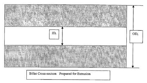
FIG. 1 is a schematic view of a consolidated hollow billet according to the
invention;
FIG. 2 is a schematic view of a hollow billet being extruded according to
the present invention for extrusion of a tube;
FIGS. 3A, 3B and 3C show electron backscatter diffraction (EBSD)
electron micrographs relative to the longitudinal (z), radial (ND) and
tangential (x)
directions, respectively, of a tubular sputtering target according to the
present
invention;
FIG. 4 shows the EBSD micrograph of 3B under higher magnification;
F1G. 5 shows the EBSD Pole Figure analysis of a tubular sputtering target
according to the present invention;
FIG. 6 shows the EBSD Inverse Pole Figure analysis of a tubular
sputtering target according to the present invention;
FIG. 7 is a schematic showing a solid billet being extruded according to
the invention for intermediate work pieces;
FIGS. 8A and 8B show schematic views of upset forging a billet according
to the present invention;
FIGS. 9A and 9B show sputtering target plates according to the present
invention being cut from forged billets; and
FIGS. l0A and 10B show a billet being hammer forged according to one
embodiment of this invention.
CA 02577162 2007-02-14
WO 2006/026621 PCT/US2005/030852
6
DETAILED DESCRIPTION OF THE INVENTION
Other than in the operating examples or where otherwise indicated, all
numbers or expressions referring to quantities of ingredients, reaction
conditions,
etc., used in the specification and claims are to be understood as modified in
all
instances by the term "about." Various numerical ranges are disclosed in this
patent application. Because these ranges are continuous, they include every
value
between the minimum and maximum values. Unless expressly indicated
otherwise, the various numerical ranges specified in this application are
approximations.
As used herein, the term "banding" refers to non-uniformities in the grain
or texture, the grain size, or grain orientation that occur in a strip or
pattern along
the surface of the sputtering target. As used herein, the term "through
thickness
gradient" refers to changes in grain or texture, grain size, or grain
orientation
moving from the edge of the target to the center of the target.
The forms of molybdenum, sputtering targets described herein below are
characterized as having no or minimal banding or through thickness gradient.
As such, the present invention is directed to molybdenum sputtering targets
having fine, uniform grain size as well as uniform texture, substantially free
of
both texture banding and through thickness gradient from a center to an edge
of
the target, with high purity and optionally micro-alloyed for improved
performance.
In the present invention, the molybdenum sputtering targets are very pure,
as such, the molybdenum sputtering targets have a purity of at least 99.5%, in
some cases 99.9%, n other cases 99.95%, in some instances at least 99.99% and
in
other instances at least 99.999%. As used herein, the term "purity" refers to
the
weight percentage of molybdenum in the sputtering target.
The present invention provides a tubular-shaped sputtering target and its
method of manufacture. The present method involves the use of pure
molybdenum powder as a starting material, and its consolidation to a
substantially
fully dense article in the form of a tube. The tubular form produced has a
fine,
uniform grain size, and a texture which is substantially uniform throughout,
and
does not change from tube to tube. Such tubular forms yield thin films that
have
CA 02577162 2007-02-14
WO 2006/026621 PCT/US2005/030852
7
trie required purity, and a thickness which is both easily predictable and
uniform
across the area of a given substrate.
ln an embodiment of the invention, the tubular-shaped sputtering target
has a texture that is substantially free of banding and substantially free of
any
through thickness gradient.
According to the present invention, a tubular-shaped sputtering target is
formed by the pressing and sintering of molybdenum powder to form a billet,
removing the center of the billet, working the billet, and heat treating the
billet to
form a tubular-shaped sputtering target.
In the present invention, ammonium dimolybdate is selected to meet
required purity specifications, and then reduced to molybdenum metal powder in
hydrogen using conventional hydrogen reduction processes. The ammonium
dimolybdate can be at least 95% pure, in some cases at least 99% pure, in
other
cases at least 99.5% pure and in certain instances 99.999% pure. The purity of
the
ammonium dimolybdate can range between any of the values recited above.
Typically, the molybdenum powder is placed in a mold and the powder is
pressed at a pressure of at least 16 ksi, in some cases at least 30 ksi and in
other
cases at least 32 ksi. Also, the powder can be pressed at a pressure of up to
40 ksi,
in some cases up to 37 ksi and in other cases up to 35 ksi. The molybdenum
powder in the mold can be pressed at any pressure recited above or at
pressures
ranging between any of the pressures recited above.
Further, when the pressed billet is sintered in the mold, it is sintered at a
temperature of at least 1785 C, in some cases at least 1800 C and in other
cases at
least 1850 C. Also, the pressed billet can be sintered at a temperature of up
to
2200 C, in some cases up to 2175 C and in other cases up to 2150 C. The
pressed molybdenum billet in the mold can be sintered at any temperature
recited
above or at temperatures ranging between any of the temperatures recited
above.
In an embodiment of the invention, the pressing is performed isostatically.
In another embodiment of the invention, the powder is sintered in hydrogen.
As shown in FIG. 1, the center of the consolidated billet is removed
through trepanning such that the ID, is smaller than the inside diameter of
the
finished tubular form. The ODi is selected such that the ratio of reduction in
CA 02577162 2007-02-14
WO 2006/026621 PCT/US2005/030852
8
cross-sectional area normal to the billet length is at least 3:1, in some
cases at least
3.5:1 and in other cases at least 4:1. Also, the reduction in cross-sectional
area
normal to the billet length can be up to 12:1, in some cases up to 10:1 and in
other
cases up to 8:1. In a particular embodiment of the invention, the reduction in
cross-sectional area normal to the billet length is 4.9:1 or higher. The
reduction in
cross-sectional area normal to the billet length can be any of the values or
range
between any of the values recited above.
The tubular billet is worked to form a worked billet having an inner
diameter ID and an outer diameter ODf such that the ratio of ODI to ODf is as
described above.
In an embodiment of the invention, the tubular billet is worked by extruding
the
billet, as shown in FIG. 2. In this embodiment, the billet is extruded with a
reduction ratio (created by the change of OD, to ODf) in cross-sectional area
as
described above. The billet length may be variable. The product form ID is
controlled through the use of mandrel tooling.
In a particular embodiment of the invention, the tubular billet can be
extruded at a temperature of at least 925 C, in some cases at least 950 C, and
in
other cases at least 1000 C. Also, the tubular billet can be extruded at a
temperature of up to 1370 C, in some cases up to 1260 C and in other cases up
to
1175 C. The tubular billet can be extruded at any temperature recited above or
at
a temperature ranging between any of the temperatures recited above.
In another embodiment of the invention, the working, i.e., reduction ratio
(created by the change of ODi to ODf) in cross-sectional area, is achieved
through
a rotary forging process that replaces the extrusion.
In an embodiment of the invention, after working the billet, it is heat
treated at a temperature of at least 815 C, in some instances at least 925 C,
in some
cases at least 950 C and in other cases at least 1000 C. Also, the heat
treatment
can be carried out at up to 1375 C, in some cases up to 1260 C and in other
cases
up to 1175 C. The heat treatment can be at any temperature or range between
any
temperatures recited above.
CA 02577162 2007-02-14
WO 2006/026621 PCT/US2005/030852
9
In a particular embodiment of the invention, the heat treatment is carried
out at from 1250 to 1375 C.
In another particular embodiment of the invention, the heat treatment is
carried out at from 815 to 960 C.
While not wishing to be limited to any single theory, under some heat
treatment conditions, it is believed that subjecting the extruded tubular
form to heat treatment results in recrystallization, yielding a strain-free,
equiaxial grain structure.
However, in some embodiments of the invention, the heat treatment is
applied for "stress-relief' purposes only.
After heat treatment, the tubular form is machined to its final dimensions.
In an embodiment of the invention, the tubular-shaped sputtering target
has a uniform texture which is a 110 orientation parallel to the longitudinal
direction and a 111 orientation relative to the radial direction.
As indicated above, the present invention provides a source of
molybdenum in the form of a tube. The tube can be used in a sputtering process
whereby thin films are deposited on a substrate. In many cases, the components
containing thin-film-deposited substrates are used in a flat panel display
(FPD).
The invention provides molybdenum in a form and with properties which were not
previously available, allowing improvements in the manufacturability and the
performance of the FPD's.
A particular advantage of the present tubular-shaped sputtering target is its
uniform texture. The crystallographic texture of a tube made according to the
invention was determined and is detailed below.
FIGS. 3A, 3B and 3C show the texture of the sample relative to the
longitudinal (z), radial (ND) and tangential (x) directions, respectively.
FIG. 4
shows the top part of FIG. 3B at higher magnification, so the grains can be
distinguished. FIG. 5 shows the Pole Figures, and FIG. 6 shows the Inverse
Pole
Figures.
The material is fully recrystallized and strain-free, as seen by the fact that
there is no significant color variation within each grain. The texture is well
defined, but not very strong (the highest peak is 3.6 times random). The most
CA 02577162 2007-02-14
WO 2006/026621 PCT/US2005/030852
obvious component of texture is 110 parallel to the longitudinal direction, as
seen
by the predominant red in FIG. 3A. Another noticeable feature is a sharp 111
peak parallel to the radial direction. There is only the slightest variation
of texture
with radius. There is no banding of texture at all. The fine, uniform grain
size,
5 and the uniformity of texture through the thickness of the tube and along
the
length of the tube are features which distinguish the present invention from
the
prior art. These features allow for more uniform film deposition during
sputtering
operations.
Thus, the present invention provides a sputtering target having a uniform
10 and fine texture and grain structure. In an embodiment of the invention,
the grain
size is at least 22 m, and in some cases at least 45 m. More importantly,
however, the average grain size is not more than 125 m, in some cases not
more
than 90 m and in other cases not more than 65 m. When the grain size is too
large, thin films formed from sputtering the present sputtering target will
not have
the desired uniform texture and/or film thickriess. The grain size in the
present
sputtering target can be any value or range between any values recited above.
Embodiments of the invention are also directed to a novel method of
manufacturing molybdenum sputtering targets, which produces performance
superior to that which is presently known in the art. This method of
manufacture
involves the use of pure molybdenum powder as a starting material and its
consolidation to a substantially fully dense article in the form of a plate.
The
inventive plate, which is produced through a multi-directional
thermomechanical
working process as described below, has a fine, uniform grain size and a
texture
which is substantially uniform throughout the plate. Such plates yield thin
films
that have the required purity, and a thickness that is both easily predictable
and
uniform across the area of the substrate.
In an embodiment of the invention, the plates have a texture that is
substantially
free of banding and substantially free of any through thickness gradient.
In the present multi-directional thermomechanical working process,
ammonium dimolybdate is reduced to molybdenum metal powder in hydrogen
using methodologies well known in the art. In an embodiment of the invention,
CA 02577162 2007-02-14
WO 2006/026621 PCT/US2005/030852
11
the ammonium dimolybdate is 99.95%, in some cases 99.9% and in other cases
99.5% pure.
Thus, in a first step I), the molybdenum powder is placed in a mold and
pressed at a pressure of at least 100 MPa, in some cases at least 200 MPa and
in
other cases at least 250 MPa. Also, the powder can be pressed at a pressure of
up
to 275 MPa. The molybdenum powder in the mold can be pressed at any pressure
recited above or at pressures ranging between any of the pressures recited
above.
Further, after the molybdenum powder is pressed in the mold, it is sintered
at a temperature of at least 1785 C. Also, the powder can be sintered at a
temperature of up to 2175 C, in some cases up to 2200 C. The pressed
molybdenum workpiece can be sintered at any temperature recited above or at
temperatures ranging between any of the temperatures recited above.
In an embodiment of the invention, the pressing is performed isostatically.
In another embodiment of the invention, the pressed powder is sintered in
hydrogen. Thus, the molybdenum metal powder can be placed in a rubber mold,
isostatically pressed and the pressed piece then sintered in hydrogen to form
a
billet with a cross-sectional area which can be from 1.5 to 4, in some cases
from 2
to 3, and in a particular embodiment approximately 2.4 times the size of the
intended target cross-sectional area of the eventual sputtering target. In
other
words, the billet has a diameter of D .
The billet is then preheated, prior to extruding, to a temperature of at least
900 C, in some cases 925 C and in other cases at least 950 C. Also, the billet
can
be preheated to a temperature of up to 1260 C, in some cases 1225 C and in
other
cases up to 1175 C. The preheated temperature can be any value or can range
between any values recited above.
As shown in FIG. 7, the billet is extruded to form an extruded billet having
a diameter of D2, such that the ratio of reduction (D :D2) in cross-sectional
area is
at least 2.5:1, in some cases at least 3:1 and in other cases at least 3.5:1.
Also, the
ratio of reduction can be up to 12:1, in some cases 10:1 and in other cases up
to
8:1. The ratio of reduction can be any value or range between any values
recited
above. The billet length can be variable.
CA 02577162 2007-02-14
WO 2006/026621 PCT/US2005/030852
12
In an alternative embodiment, rotary forging or hammer forging can be
used in place of the extrusion operation to provide a billet with the
aforementioned ratio of reduction (D :D2) in cross-sectional area.
In order to prepare the extruded billet for upset forging, it is subjected to
a
first heat treatment step. This heat treatment step generally provides stress
relief.
The first heat treatment is conducted at a temperature of at least 800 C, in
some
cases at least 815 C, in some cases at least 830 C and in other cases at a
temperature of at least 850 C. Also, the first heat treatment can be conducted
at a
temperature up to 960 C, in some cases up to 930 C and in other cases up to
900 C. The temperature of the first heat treatment step can be any value
recited
above or can range between any values recited above.
The billet is also cut to a length so that it will not buckle. In an
embodiment of the invention, the billet is cut to a length such that the
billet's
aspect ratio (Length/Diameter) is less than or equal to 2.0, in some cases
less than
or equal to 1.6.
After the first heat treatment and before upset forging, the heat-treated
extruded
billet is preheated to a temperature of at least 900 C, in some cases at least
925 C,
in other cases at least 950 C, in some situations at least 975 C and in other
cases
at least 1000 C. Also, the heat-treated extruded billet can be preheated to a
temperature of up to 1300 C, in some cases up to 1260 C, in other cases up to
1200 C and in some instances up to 1150 C. Prior to upset forging, the heat-
treated extruded billet can be preheated to any temperature recited above or
can
range between any temperature recited above.
As shown in FIGS. 8A and 8B, the heat-treated extruded billet is subjected
to upset forging such that the ratio of D2, the heat-treated extruded billet
cross-
sectional area, to Df, the forged billet cross-sectional area, is from 1:1.5
to 1:3, in
some cases 1:1.75 to 1:2.5, and in other cases from 1:1.8 to 1:2.25. In an
embodiment of the invention, the ratio of D2 to Df is approximately 1:2 0.2.
Specifically, FIG. 8A shows the billet at the start of the upset forging
process and
FIG. 8B shows the billet at the end of the upset forging process.
The upset forging of the extruded billet is carried out at a temperature of at
least 800 C, in some cases at least 900 C, in other cases at least 925 C and
in
CA 02577162 2007-02-14
WO 2006/026621 PCT/US2005/030852
13
some instances at least 950 C. Also, the upset forging of the extruded billet
can
be carried out at up to 1300 C, in some cases up to 1260 C, in other cases up
to
1200 C, in some instances up to 1100 C and in other instances up to 1000 C.
The
forging temperature allows the billet to be forged to form a forged billet
having a
diameter Df as described above. The forging temperature can be any temperature
described above or can range between any of the temperatures recited above.
After forging, the forged billet is subjected to a second heat treatment step.
The second heat treatment step is a recrystallization step that provides a
strain-free
equiaxial grain structure. The second heat treatment is conducted at a
temperature
of at least 1200 C, in some cases at least 1250 C, in some cases at least 1275
C
and in other cases at a temperature of at least 1300 C. Also, the second heat
treatment can be conducted at a temperature up to 1400 C, in some cases up to
1375 C and in other cases up to 1350 C. The temperature of the second heat
treatment step can be any value recited above or can range between any values
recited above.
In an alternative embodiment, the second heat treatment provides stress
relief only and not recrystallization. In this embodiment, the heat treatment
is
carried out at a temperature of at least 800 C, in some cases 815 C and in
other
cases at least 850 C. Also, the heat treatment can be carried out at a
temperature
of up to 1000 C, in some cases up to 960 C and in other cases up to 925 C. The
temperature of the second heat treatment step under this embodiment can be any
value recited above or can range between any values recited above.
As indicated above, the second heat treatment is applied at a temperature
and for a time that provides a billet that has a strain-free equiaxial grain
structure.
Thus, after the second heat treatment, a billet is provided that is completely
recrystallized and strain free.
As shown in FIG. 9A, material affected during upset forging by the
centering disks (CD) is removed. The material affected by the centering disks
is
not generally usable as target material. Sputtering targets are sliced from
the billet
according to the orientation shown in FIG. 9B. The entirety of the billet is
usable
as target once the centering disk affected material is removed.
CA 02577162 2007-02-14
WO 2006/026621 PCT/US2005/030852
14
In an alternative embodiment as shown in FIGS. l0A and IOB, the upset
forging operation is replaced by a hammer/upset forging such that the ratio of
D2,
the heat-treated extruded billet cross-sectional area, to Df, the forged
billet cross-
sectional area, is as described above. FIG. l0A shows the billet at the start
of the
hammer forging operation and FIG. lOB shows the billet after the hammer
forging
operation. After the hammer forging operation, the billet is given a second
heat
treatment as described above. In other words, a disc-shaped portion is cut
from
the heat-treated forged billet to provide a disc-shaped sputtering target.
The grain and texture of the resulting sputtering target is generally
analyzed using electron backscatter diffraction (EBSD). Because of the above-
described process, the grain and texture from target to target is very
consistent.
The targets are typically sampled from the center, mid-radius, and edge on the
XZ
plane, i.e., the radial-axial plane.
In an embodiment of the present invention, a sputtering target is provided
having a uniform and fine texture and grain structure. In an embodiment of the
invention, the grain size is at least 22 gm and in some cases at least 65 m.
More
importantly, however, the average grain size is not more than 125 m, in some
cases not more than 90 gm and in other cases not more than 65 gm as determined
by electron backscatter diffraction. When the grain size is too large and/or
non-
uniform, thin films formed from sputtering the present sputtering target will
not
have the desired uniform texture and/or film thickness. The grain size in the
present sputtering target can be any value or range between any values recited
above.
The present invention also provides a method of making a sputtering target
including the steps, as described above, of:
I) placing molybdenum powder in a mold and pressing the powder at
the pressures indicated above and sintering the pressed piece at
temperatures indicated above to form a billet having a diameter of
Do;
II) extruding the billet to form an extruded billet having a diameter of
D2 such that the ratio of Do to D2 is as indicated above;
CA 02577162 2007-02-14
WO 2006/026621 PCT/US2005/030852
III) applying a first heat treatment to the extruded billet at the
temperatures indicated above;
IV) upset forging the extruded billet at the temperatures indicated
above to form a forged billet having a diameter Df such that the
5 ratio of Df to D2 is as indicated above;
V) applying a second heat treatment to the forged billet at the
temperatures indicated above; and optionally
VI) cutting a disc-shaped portion from the heat-treated forged billet to
provide a disc-shaped sputtering target.
10 Embodiments of the invention provide large molybdenum plates having a
non-segmented construction. As used herein, the term "non-segmented" refers to
plates made in one piece and not to plates made by combining or joining two or
more plates. Typically, the present plates weigh at least 300 kg, in some
cases at
least 350 kg and in other cases at least 400 kg. The plates according to the
15 invention include at least 99%, in some cases at least 99.5% and in other
cases at
least 99.9% by weight of molybdenum.
In an embodiment of the invention, the large molybdenum plates have a
fine, uniform grain size where the average grains are not more than 100 m, in
some cases not more than 60 m, and in other cases not more than 20 m. In
this
embodiment, the grain size can be at least 5 m and in some cases at least 10
m.
The grain size can be any value recited above or range between any values
recited
above.
In an embodiment of the invention, the large molybdenum plates include a
backing plate to provide support.
ln another embodiment of the invention, the large plate has a texture that is
substantially free of banding and substantially free of any through thickness
gradient.
In an embodiment of the invention, the plates have a rectangular cross-
sectional
shape and have a length of at least 0.8 m, in some cases at least 1.2 m and in
other
cases at least 2 m and up to 2.6 m, in some cases up to 3.4 m and in other
cases up
to 4 m; a width of at least 0.7 m, in some cases at least 0.9 m and in other
cases at
least 1.2 m and up to 1.7 m, in some cases up to 2.0 m and in other cases up
to 2.5
CA 02577162 2007-02-14
WO 2006/026621 PCT/US2005/030852
16
in; and a height (thickness) of at least 0.008 m, in some cases at least 0.012
m and
in other cases at least 0.018 m and up to 0.020 m, in some cases up to 0.032 m
and
in other cases up to 0.064 m. The dimensions of the rectangular plate can be
any
of the values recited above and can range between any of the values recited
above.
In another embodiment of the invention, the plates have a square cross
sectional shape and have a length of at least 0.8 m, in some cases at least
1.0 m
and in other cases at least 1.2 m and up to 1.6 m, in some cases up to 2.0, in
some
situations up to 2.5 m, and in other cases up to 3.0 m; a substantially equal
width
and height (thickness) of at least 0.008 m, in some cases at least 0.012 m and
in
other cases at least 0.018 m and up to 0.020 m, in some cases up to 0.032 m
and in
other cases up to 0.064 m. The dimensions of the square plate can be any of
the
values recited above and can range between any of the values recited above.
In another embodiment of the invention, a portion can be cut from the
plate to form either a circular or cylindrical cross-sectional shaped portion
having
a length (thickness) of at least 0.008 m, in some cases at least 0.010 m and
in other
cases at least 0.012 m and up to 0.018 m, in some cases up to 0.032 m and in
other
cases up to 0.064 m; and a diameter of at least 0.7 m, in some cases at least
0.9 m
and in other cases at least 1.2 m and up to 1.75 m, in some cases up to 2.0 m,
in
other cases up to 2.5 m, and in some instances up to 3.0 m. The dimensions of
the
circular portion can be any of the values recited above and can range between
any
of the values recited above.
As is known in the art and regardless of the particular shape of the
sputtering target, when the dimensions of the sputtering target reach a size
where
support is needed, a backing plate is included with the sputtering target.
In making the large molybdenum plate according to the invention,
molybdenum powder is used. The powder is prepared by thermal and hydrogen
reduction of ammonium molybdate that is at least 99%, in some cases at least
99.5% and in other cases at least 99.9% pure to produce molybdenum metal
powder. The powder is typically screened to produce a particle morphology and
size distribution to sinter. The particle size typically has a weight average
value
of at least 0.1 m, in some cases at least 0.5 m, in other cases at least 1
m, in
some instances at least 5 m, in other instances at least 10 m, in some
situations
CA 02577162 2007-02-14
WO 2006/026621 PCT/US2005/030852
17
at least 15 m and in other situations at least 20 m. Also, the particle size
typically has a weight average value and up to 150 m, in some cases up to 125
m, in other cases up to 100 m, in some instance up to 75 m, in other
instances
up to 50 m and in some situations up to 40 m. The particle size of the
powder
can be any of the values recited above and can range between any of the values
recited above.
The particle morphology can typically be described as irregularly-shaped
agglomerates of fine particles.
The molybdenum powder is poured into a sheet bar mold and
jolted/tapped.
The molybdenum powder is then consolidated by cold isostatic pressing (CIP) at
a
pressure of at least 100, in some cases at least 125 and in other cases at
least 150
Mpa. Also, the CIP pressure can be up to 250, in some cases up to 225, and in
other cases up to 200 Mpa. The CIP pressure is a pressure sufficient to form a
sheet bar. The CIP pressure can be any value recited above or range between
any
values recited above.
After the CIP process, the sheet bar is sintered at a temperature of at least
1600 C, in some cases 1650 C and in other cases at least 1700 C. Also, the
sintering temperature can be up to 1800 C, in some cases up to 1750 C and in
other cases up to 1725 C. The sintering temperature is a temperature
sufficient to
form an ingot having a density of at least 90% of the theoretical density. The
sintering temperature can be any temperature or range between any temperatures
recited above.
The sintering is performed for at least 4, in some cases at least 10 and in
other cases at least 16 hours. Also, the sintering is performed for up to 32,
in
some cases up to 24 and in other cases up to 20 hours. The time for sintering
is a
length of time sufficient to achieve at least 90% of the theoretical density.
The
length of time for sintering can be any value recited above or range between
any
values recited above.
The sintered bar, or ingot, is preheated to a temperature of at least 1100 C,
in
some cases at least 1150 C and in other cases at least 1200 C. Also, the ingot
can
be preheated to a temperature of up to 1450 C, in some cases up to 1350 C and
in
CA 02577162 2007-02-14
WO 2006/026621 PCT/US2005/030852
18
other cases up to 1300 C. The ingot can be preheated to any temperature or
range between any temperatures recited above.
The preheated ingot is hot rolled at a temperature of at least 1050 C, in
some cases at least 1100 C and in other cases at least 1150 C. Also, the ingot
can
be hot rolled at a temperature of up to 1400 C, in some cases up to 1300 C and
in
other cases up to 1250 C. The hot rolling effects a reduction in the thickness
and
an increase in the length of the ingot. The hot rolling temperature can be any
value or range between any value recited above.
The reduction achieve from hot rolling can be at least 50%, in some cases
75% and in other cases at least 98% of the thickness of the pre-hot rolled
ingot.
Also, the length of the ingot can increase at least 50%, in some cases at
least 75% and in other cases at least 150% and can increase up to 300%, in
some
cases up to 400% and in other cases up to 500%. The length of the ingot can
increase to any value or range between any of the values recited above.
The thickness of the hot rolled ingot can be further reduced by subsequent
reduction, maintaining the integrity of the plate. The subsequent reduction
can be
at least 10%, in some cases at least 15% and in other cases at least 20% and
can be
up to 30%, in some cases up to 28% and in other cases up to 25% of the hot
rolled
ingot thickness. The subsequent reduction can be any value or range between
any
of the values recited above.
During the rolling reduction process, the plates can be reheated to maintain
the temperatures indicated above. Typically, the plates are inspected for
integrity
throughout the rolling process. Also, the plates can be precision leveled to
achieve optimum flatness for subsequent machining/grinding operations in order
to achieve the desired final dimensions.
The roll reduced ingot is heat treated at a temperature of at least 850 C, in
some cases at least 860 C and in other cases at least 880 C and can be up to
950 C, in some cases up to 920 and in other cases up to 900 C. This heat
treatment step can be carried out any temperature or range between any of the
temperatures recited above.
The roll reduced ingot heat treatment is performed for at least 30 minutes,
in some cases at least 45 minutes and in other cases at least 60 minutes.
Also, the
CA 02577162 2007-02-14
WO 2006/026621 PCT/US2005/030852
19
heat treatment can be performed for up to 180 minutes, in some cases up to 120
minutes and in other cases up to 90 minutes. The length of time for the heat
treatment can be any value recited above or range between any values recited
above.
During or after the above-described process, the integrity of an ingot can
be conducted using ultrasonic techniques.
In an embodiment of the invention, in preparing any of the sputtering
targets described above, microalloys can be included in the molybdenum powder
prior to pressing. Non-limiting examples of suitable microalloys include those
comprising one or more metallic materials selected from Ta, Nb, Cr, W and/or
V.
In a particular embodiment of the invention, the microalloy has a body-
centered
cubic (BCC) structure.
When microalloys are used they are typically processed by adding one or
more metallic materials into the molybdenum powder before the powder pressing
stage described above. The described steps in forming ingots or billets are
followed as indicated above.
When microalloys are used, they are included in amounts that provide the
particular properties desired. As such, the metallic materials can be included
at up
to 1000 ppm, in some cases up to 750 ppm, in other cases up to 500 ppm, in
some
situations up to 300 ppm, in other situations up to 150 ppm, and in some
instances
up to 75 ppm. Also, when included, the metallic materials can be included at a
level of at least 10 ppm, in some cases at least 20 ppm and in other cases at
least
ppm.
When microalloys are included, they are typically included to provide
25 particular affects on the molybdenum that is finally produced. As a non-
limiting
example, the molybdenum can take on a BCC structure by intentionally adding W,
V and/or Cr or combinations thereof. These BCC metallic elements, when
included with the molybdenum, create a localized lattice stress. The stress
decreases the energy barrier for (a) atoms leaving the sputtering targets when
sputtering (i.e. increasing the sputtering rates of the targets), and (b) the
etch of
thin film during photolithographic processes (for example by either liquid
etch or
dry etch, such as by plasma etch or reactive etch). When the microalloy is
CA 02577162 2007-02-14
WO 2006/026621 PCT/US2005/030852
included, it is included at a level that provides the above-described effect,
but not
at a level that would compromise any properties of the film produced.
Additionally, the present invention provides a method of sputtering,
whereby any of the above-described sputtering targets are subjected to
sputtering
5 conditions and are thereby sputtered.
Any suitable sputtering method can be used in the present invention.
Suitable sputtering methods include, but are not limited to, magnetron
sputtering,
pulse laser sputtering, ion beam sputtering, triode sputtering, and
combinations
thereof.
10 The present invention also provides a method of making a thin film
including the steps of:
(a) sputtering the above-described sputtering target;
(b) removing Mo atoms from the target; and
(c) forming a thin film comprising molybdenum onto a substrate.
15 In an embodiment of the invention, after (b), a step including supplying a
reactive gas to the Mo can be added. A reactive gas is a gas that includes a
component that can react with the molybdenum either in a gaseous state or once
deposited onto a substrate to form a molybdenum compound. As a non-limiting
example, the reactive gas can be oxygen, nitrogen and/or a silicon containing
gas.
20 The thin film applied by the present method can have any desired
thickness. The thickness of the thin film will depend on the end use
application
desired. Typically, the thickness of the thin film can be at least 0.5 nm, in
some
situations I nm, in some cases at least 5 nm, in other cases at least 10 nm,
in some
situations at least 25 nm, in other situations at least 50 nm, in some
circumstance
at least 75 nm and in other circumstances at least 100 nm. Also, the film
thickness
can be up to 10 m, in some cases up to 5 m, in other cases up to 2 m, in
some
situations up to 1 m and in other situations up to 0.5 m. The film thickness
can
be any of the stated values or can range between any of the values stated
above.
The thin film can be or be part of a flat panel display.
Due to the uniformity of grain size and texture through the thickness of the
molybdenum sputtering targets, the films obtained from such targets have
excellent uniformity.
CA 02577162 2007-02-14
WO 2006/026621 PCT/US2005/030852
21
In a particular embodiment of the invention a very thin film is provided.
In this embodiment, the thin film is at least 100 A, in some cases at least
250 A
and in other cases at least 500 A. In this embodiment, the thin film can be up
to
5,000 .A, in some cases up to 3,000 A, in other cases up to 2,500 A and in
some
situations up to 2,000 A.
Any suitable substrate may be used in the invention. Suitable substrates
for the thin film used in the flat panel display devices (FPD) include, but
are not
limited to, flexible foils, plastic substrates, glass substrates, ceramic
substrates,
and combinations thereof. The plastic substrates include, but are not limited
to,
polynorbomene, polyimide, polyarylate, polycarbonate, polyethylenenaphthanate
(PEN), polyethyleneterephthalate (PET), and the like. A non-limiting example
of
a ceramic substrate includes sapphire.
In addition to molybdenum thin films on various substrates, MoOX
(oxidation), MoNx (nitridation), MoSi, (silicidation) can also be produced by
reactive sputtering or ion implantation.
The invention encompasses products used in various applications. In one
embodiment, a thin film made in accordance with the invention can be used in
thin film transistor (TFT)-liquid crystal display (LCD) applications. Also, in
another embodiment, the invention encompasses a thin film used in solar cell
applications, sensor applications, semiconductor devices and metal gates for
CMOS technology (complementary metal oxide semiconductor). In one
embodiment, the invention is directed to a TFT- LCD device containing
molybdenum thin films that serve as gate electrodes that have excellent
uniformity. Another embodiment is directed to thin film solar cell
applications,
where the invention encompasses solar cells in which Mo thin films function as
a
back contact for the following illustrative device structure: MoOz containing
front
contact/p-layer/junction layer/n-layer/Mo back contact, in which the p-layer
releases electrons when it is struck by light, resulting in a lack of
electrons, and n-
layer is negatively charged.
In sensor applications, an MoO3 film can be produced by reactive
sputtering from a Mo target for use as a gas sensor, such as for ammonia
detection. In another embodiment, the invention encompasses either molybdenum
CA 02577162 2007-02-14
WO 2006/026621 PCT/US2005/030852
22
or nitrided molybdenum films used as gate devices for CMOS processes
(complementary metal oxide semiconductor) with a tunable work function
depending on the nitrogen-doping level.
When improving the picture quality of a FPD, increasing the contrast in
bright settings is easier than increasing display brightness. An MoO,, film
can be
used to form a black matrix by reactive sputtering from molybdenum sputtering
target to enhance image contrast. Traditionally, either Cr or Cr02 target is
used to
form a black matrix in Flat Panel Display, which has both health and
environmental concerns.
The invention and various embodiments thereof have been described
above. It will be obvious to those skilled in the art that various changes and
modifications may be made therein without departing from the scope of the
invention as defined in the specification and the appended claims.