Note: Descriptions are shown in the official language in which they were submitted.
CA 02577730 2007-01-26
INTERCONNECTED NANOSYSTEMS
FIELD OF THE INVENTION
[0001] The present invention relates generally to the field of nanotechnology,
and more
particularly, to interconnects for nanotubes, nanowires and other nanoscale
structures and
devices.
BACKGROUND INFORMATION
[0002] Essentially all devices needed to make the equivalent of a modem
digital or analog
circuit out of nanotubes and/or nanowires have been demonstrated in prototype
experiments,
and elementary logic circuits have been demonstrated. Various researchers have
claimed that
nanowire/nanotube devices are superior to CMOS in various metrics, such as
transconductance
per width or mobility. When properly phrased, these claims are true. The
underlying,
unspoken motivation remains, however, that the devices are or can be smaller
than spatial
resolution limits posed by lithography, which would provide a route to extend
Moore's law into
the domain of nanotechnology.
[0003] The nanotube and nanowire devices developed to date have been contacted
by
lithographically fabricated electrodes. This is not a scalable technique for
massively parallel
processing, integrated nanosystems, due to the geometrical limits of
lithography. The potential
high-density circuitry possible with nanowires and nanotubes will not be
realized if each
nanowire and nanotube is contacted lithographically.
[0004] Fault-tolerant architectural schemes have recently been proposed to
tackle this
interconnect problem. For example, using N lithographically fabricated wires,
it is possible to
address individually 2N nanowires using a binary-tree multiplexing scheme.
Since the spacing
between the nanowires is beyond the limits of lithography, the electrical
connections between
the nanowires and lithographically fabricated wires are random, but could in
principle be
measured after the manufacturing process. With this technique, each chip
manufactured would
have its own unique firmware, specific to the nano-level physical hardware
defects.
[0005] However, a more manufacturable interconnect is needed that allows
efficient
implementation and full scalability of integrated nanosystems.
1
CA 02577730 2007-01-26
SUMMARY
[00061 Described below are exemplary embodiments of wireless interconnects for
nanodevices and nanosystems. These embodiments are examples only and are not
intended to
limit the invention.
[0007] The devices, systems and methods described herein provide wireless
interconnects
for nanodevices and nanosystems. More specifically, communication to or from a
nanodevice
is provided with a nanostructure-based antenna, preferably formed from, but
not limited to, a
single wall nanotube (SWNT). Other nanostructure-based antenna include double
walled
nanotubes, semiconducting nanowires, metal nanowires and the like. The use of
a
nanostructure-based antenna eliminates the need to provide a physical
communicative
connection to the nanodevice, while at the same time allowing communication
between the
nanodevice and other nanodevices or outside systems.
[0008] In one embodiment, a wirelessly interconnected system includes a
nanodevice with
a nanostructure-based antenna coupled thereto and an outside system configured
to
communicate with the nanodevice using the nanostructure-based antenna. The
nanodevice is
configured to communicate over the nanostructure-based antenna,.
[0009] In another embodiment, a method of fabricating an interconnected
nanosystem
includes forming a nanodevice having a communication lead and coupling a
nanostructure-
based antenna to the communication lead. Preferably, the coupling of a
nanostructure-based
antenna to the communication lead comprises forming a carbon nanotube on the
lead.
[0010] In yet another embodiment, a method of communicating with a
nanostructured
device by wirelessly transmitting information from a first device, and
wirelessly receiving
information at a second device, wherein at least one of the first and second
devices is a nano-
structured device
[0011) In yet another embodiment, an interconnected system includes a first
device and a
second device wirelessly coupled to the first device, wherein one of the first
and second devices
is a nanodevice.
[0012] In yet another embodiment, an interconnected system includes a first
device and a
second device wirelessly coupled to the first device, wherein one of the first
and second devices
includes a nanostructure-based antenna.
[0013] The above and other preferred features, including various novel details
of
implementation and combination of elements will now be more particularly
described with
reference to the accompanying drawings and pointed out in the claims. It will
be understood
2
CA 02577730 2007-01-26
that the particular methods and apparatus are shown by way of illustration
only and not as
limitations. As will be understood by those skilled in the art, the principles
and features
explained herein may be employed in various and numerous embodiments.
BRIEF DESCRIPTION OF THE FIGURES
[0014] The details of the invention, including fabrication, structure and
operation, may be
gleaned in part by study of the accompanying figures, in which like reference
numerals refer to
like segments.
[0015] FIG. 1 depicts a schematic of one exemplary embodiment of a nano-
structure
device.
[0016] FIG. 2 depicts a block diagram of one exemplary embodiment of an
interconnected
nanosystem.
[0017] FIG. 3 depicts a block diagram of a carbon nanotube receiving antenna
and dipole
transmitting antenna.
[0018] FIG. 4 depicts a graph illustrating conductance measurements of the
carbon
nanotube receiving antenna shown in Fig. 3.
100191 It should be noted that the figures are not drawn to scale and that
elements of similar
structures or functions are generally represented by like reference numerals
for illustrative
purposes throughout the figures. It also should be noted that the figures are
only intended to
facilitate the description of the preferred embodiments.
DETAILED DESCRIPTION
[0020] Each of the additional features and teachings disclosed below may be
utilized
separately or in conjunction with other features and teachings to provide
wireless interconnects,
such as nanostructure-based antennas, for nanodevices and nanosystems.
Representative
examples of the present invention, which examples utilize many of these
additional features
and teachings both separately and in combination, will now be described in
further detail with
reference to the attached drawings. This detailed description is merely
intended to teach a
person of skill in the art further details for practicing preferred aspects of
the present teachings
and is not intended to limit the scope of the invention. Therefore,
combinations of features and
steps disclosed in the following detail description may not be necessary to
practice the
invention in the broadest sense, and are instead taught merely to particularly
describe
representative examples of the present teachings.
3
CA 02577730 2007-01-26
[0021] Moreover, the various features of the representative examples and the
dependent
claims may be combined in ways that are not specifically and explicitly
enumerated in order to
provide additional useful embodiments of the present teachings. In addition,
it is expressly
noted that all features disclosed in the description and/or the claims are
intended to be disclosed
separately and independently from each other for the purpose of original
disclosure, as well as
for the purpose of restricting the claimed subject matter independent of the
compositions of the
features in the embodiments and/or the claims. It is also expressly noted that
all value ranges
or indications of groups of entities disclose every possible intermediate
value or intermediate
entity for the purpose of original disclosure, as well as for the purpose of
restricting the claimed
subject matter.
[0022] The disclosure provided herein relates to United States Provisional
Patent
Application Serial No. 60/601,230, filed on August 12, 2004, which application
is incorporated
herein by reference as if set forth in full.
[0023] The devices, systems and methods described herein provide wireless
interconnects
for nanodevices and nanosystems. More specifically, communication to or from a
nanodevice
is provided with a nanostructure-based antenna, preferably formed from, but
not limited to, a
single wall nanotube (SWNT). Other nanostructure-based antenna include double
walled
nanotubes, semiconducting nanowires, metal nanowires and the like. The use of
a
nanostructure-based antenna eliminates the need to provide a physical
communicative
connection to the nanodevice, while at the same time allowing communication
between the
nanodevice and other nanodevices or outside systems, i.e., systems larger than
nanoscale such
as those formed from semiconductor fabrication processes such as CMOS, GaAs,
bipolar
processes and the like.
[0024] Nanostructure-based antennas can be used for other antenna applications
as well,
including, but not limited to RFID applications. In some cases, each
nanostructure, i.e.,
nanotube or nanowire, can be a separate antenna. In other cases, the
nanostructure can be just
part of an antenna. For example, nanotubes can be used as components of
composite materials
wherein the nanotube-based composite material serves as the antenna.
[0025] FIG. 1 depicts an exemplary embodiment of a nanodevice 10 capable of
wireless
communication. The nanodevice 10 has multiple nanostructure-based antennas 16,
such as
nanotube antennas, that together form antenna arrays 11 extending from each of
the four sides
of the nanodevice 10. Preferably, each nanotube antenna 16 within the arrays
11 has a separate
resonant frequency and is configured to communicate over a separate wireless
frequency
4
CA 02577730 2007-01-26
channel corresponding to that resonant frequency. In this manner, a
multichannel
communication signal transmitted from another device or outside system can be
received by the
nanodevice 10. Because each nanotube 16 within the array s 11 receives
information on a
separate channel, each of the array 11 can act as a communication port where
each antenna 16
effectively acts as an input/output connection.
[0026] For instance, in this embodiment, the nanodevice 10 has fourteen
circuit inputs 18
per device side, each connected to a separate nanotube antenna 16. The input
signals for each
of these inputs 18 are transmitted from another device or outside system on
fourteen separate
channels so that each nanostructure-based antenna 16 receives only the
communications
transmitted over the respective resonant frequency. This allows the transfer
of separate, unique
amounts of information to each individual input 18 via the respective
nanostructure-based
antennas 16.
[0027] The nanodevice 10 can have any number of nanotube antennas 16
configured to
receive, transmit or both. In embodiments where each nanotube antenna 16 is
tuned to a
separate resonant frequency, the number of nanotube antennas 16 available to
receive data on
separate channels is limited only by the available bandwidth.
[0028] The nanodevice 10 can be any nanoscale device, or device having
nanoscale
components. The internal structure 12 of the nanodevice 10 can range from
simple nanotubes
or nanoelectrodes to more complex integrated nanosystems having nanotubes,
nanowires,
nanotransistors, self-assembling DNA and the like. Furthermore, the term
nanoscale is not
intended to limit the systems and methods herein but instead to facilitate
reference to any
apparatus, structure, device, thing or object measured with reference to
nanometers. One of
skill in the art will readily recognize that the term nanoscale can include
structures that are less
than one nanometer in size, while also including structures that are greater
than 1000
nanometers in size.
[0029] The nanostructure-based antennas 16 can be formed from any nanoscale
structure
that acts as an antenna. In a preferred embodiment, nanostructure-based
antennas 16 are
formed from carbon single walled nanotubes (SWNTs). Each carbon SWNT antenna
16 can be
tuned to a resonant frequency by adjustment of it's length. For instance, a
one centimeter
carbon SWNT antenna 16 has a resonant frequency of 4 Gigahertz.
[0030] In a preferred embodiment, a carbon SWNT antenna is formed or grown, as
described in greater detail in copending Application Serial No. (attorney
docket
no. 703538.4093, filed August 5, 2005, entitled "SYNTHESIS OF SINGLE-WALLED
CA 02577730 2007-01-26
CARBON NANOTUBES" is incorporated herein by reference, in a single furnace
system
comprising a modified CVD reaction chamber which reduces the turbulence of the
gas flow of
the hydrocarbon source provided during the growth phase. The reduced
turbulence creates an
enhanced environment for ultra-long nanotube formation. In addition, a raised
platform,
comprising an underlayer of metal, is deposited onto a substrate. The raised
platform allows
the nanotube to grow freely suspended from the substrate in the low turbulence
gas flow. This
reduces any steric force impedance caused by the substrate and enables the
nanotube to be
grown to lengths on the order of centimeters.
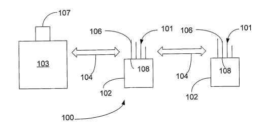
[0031) FIG. 2 depicts an exemplary embodiment of an interconnected nanosystem
100,
including nanodevices 102 and an outside system 103. Here, each nanodevice has
multiple
nanotube antennas 106 that together form an nanotube antenna array 101.
Preferably, each
nanotube antenna 106 within the array 101 has a separate resonant frequency
and is configured
to communicate over a separate wireless frequency channel corresponding to
that resonant
frequency. In this manner, a multichannel communication signal transmitted
from outside the
outside system 103 via an antenna 107 can be received by the nanodevice 102.
Because each
nanotube 106 within the array 101 receives information on a separate channel,
array 101 can
act as a communication port where each antenna 106 effectively acts as an
input/output
connection.
[0032] For instance, in this embodiment each nanodevice 102 has four circuit
inputs 108,
each connected to a separate nanotube antenna 106. The input signals for each
of these inputs
108 are transmitted from the outside system 103 on four separate channels over
communication
path 104 so that each nanostructure-based antenna 106 receives only the
communications
transmitted over the respective resonant frequency. This allows the transfer
of separate, unique
amounts of information from the outside system 103 to each individual input
108 via the
respective nanostructure-based antenna 106.
[0033] The interconnected nanosystem 100 is not limited to communication
solely between
the outside system 103 and a nanodevice 102. Each of the nanodevices 102 can
communicate
with other nanodevices 102 in a similar manner over communication path 104.
[0034] Each nanodevice 102 can have any number of nanotube antennas 106
configured to
receive, transmit or both. In embodiments where each nanotube antenna 106 is
tuned to a
separate resonant frequency, the number of nanotube antennas 106 available to
receive data on
separate channels is limited only by the available bandwidth in communication
path 104 or
6
CA 02577730 2007-01-26
each individual channel. However, other techniques can be used to increase the
data
transferring capacity of system 100, such as time or code signal multiplexing
and the like.
[0035] Antenna Experiment: As shown in Fig. 3, an unbalanced dipole
transmitting
antenna, which is resonant at f=2.8GHz, was placed about 2 inches from a
sample comprising a
carbon nanotube receiving antenna with electrode spacing of 200 micrometers.
The nanotube
antenna was formed in accordance with the method described above.
[0036] In examining the nanotube receiving antenna, using a lock-in amplifier,
the
nanotube current was measured as a function of the RF radiation field being ON
or OFF and
whether the field was applied at the transmitting antenna's resonant frequency
(fr-2.8GHz) or
not (f=1GHz). The transmitting antenna was driven at a single frequency in CW
mode with a
power of +5dBm by a network analyzer.
[0037] The measured data, shown in Fig. 4, indicates there is a 0.3
millisiemens decrease in
the nanotube's DC conductance when RF radiation at the resonant frequency of
the
transmitting antenna (f=2.8GHz) was applied to the receiving nanotube antenna.
When the
transmitting antenna is driven at a frequency far removed from its resonance,
e.g. f=1GHz, no
change in the CNT's conductance was noticed, because the transmitting antenna
efficiency was
low. These results indicate that the CNT on the sample is acting as a
receiving antenna.
[0038] In the foregoing specification, the invention has been described with
reference to
specific embodiments thereof. It will, however, be evident that various
modifications and
changes may be made thereto without departing from the broader spirit and
scope of the
invention. For example, each feature of one embodiment can be mixed and
matched with other
features shown in other embodiments. Features and processes known to those of
ordinary skill
may similarly be incorporated as desired. Additionally and obviously, features
may be added
or subtracted as desired. Accordingly, the invention is not to be restricted
except in light of the
attached claims and their equivalents.
7