Note: Descriptions are shown in the official language in which they were submitted.
CA 02577901 2007-02-22
- 1 -
External package capable of being radio-tagged
The invention relates to an external package,
particularly one enclosing a product with a radio tag,
such as an RFID (Radio Frequency IDentification) tag,
and/or in whose proximity there is such a tag.
Groceries, cigarettes, tobacco in general, chewing gum,
chocolates and much more are typically packaged in
foils which keep the content fresh. The foils are often
made of paper or another support (such as a polymer
film) onto which a thin electrically conductive layer,
normally a metal layer, typically aluminum, has been
put. In this case, the thin metal layer has quite a few
effects; among other things it has a shiny appearance,
forms a barrier layer for oxygen and moisture, reflects
the radiation of heat and has a correspondingly
insulating character.
A drawback of this external package with an
electrically conductive layer when using RFID tags,
particularly EPC (Electronic Product Code) tags and EAS
(Electronic Article Surveillance) tags, as is currently
being planned on a grand scale, is that the
electrically conductive layer of the external package
produces an electrically conductive area which shields
electromagnetic waves undesirably, in similar fashion
to in what is known as a Faraday cage, or reflects them
and hence makes it difficult or even impossible to use
radio tags and/or miscellaneous electric components on
the product and/or on the external package.
It is therefore an object of the present invention to
provide an external package having a support and an
electrically conductive layer which does not prevent
the use of tags in the surroundings of the external
package.
CA 02577901 2007-02-22
- 2 -
This object is achieved by the subject matter of the
independent and dependent claims, the description and
the figures.
The invention relates to an external package for a
product having an electric component, comprising at
least one support and an electrically conductive layer,
where the electrically conductive layer has a structure
and/or a coating which reduces the shielding produced
by its conductive area in the surroundings of the
external package such that the use of an electric
component which delivers or receives information
externally through the external package and/or whose
power supply is fed through the external package is not
adversely affected or is adversely affected only to an
extent such that the component is still operable.
In this context, the term "in the surroundings" covers
the following:
Firstly a tag which is arranged directly on the product
and/or within the external package.
Secondly a tag which is in proximity to the external
package.
The shielding by the external package means that
disturbances in the case of conventional tags within
and/or directly on the external packages and also in
the case of tags which are outside the external
package, but in proximity thereto, normally arise as a
result of the electromagnetic waves being reflected by
the metal, for example. In this context, the term "in
the surroundings" or "close" means "in the region of
the typical reading range of the tags", for example
typically up to approximately 70 cm at 13.56 MHz, and
in the case of UHF (Ultra High Frequency - 850 -
950 MHz) this may be up to approximately 2 m, and in
the GHz range even more still (several meters).
CA 02577901 2007-02-22
- 3 -
The term "that the component is still operable" means
the shielding which is still tolerable and may not
indicate a specific value, since this is dependent on
many factors such as transmission power, transmission
frequency and/or the type of component, such as the
type of radio tag. Shielding which is no longer
tolerable is a reduction in the reading distance by
half (e.g. from 70 cm to 35 cm), for example, and/or
exists when any information is shielded down to below
the noise limit and/or the power supply for a radio
frequency tag is reduced to below the minimum operating
voltage.
A shielding-reducing coating for the conductive layer
of the external package may be used as an alternative
to the structure and/or in addition to it and
preferably has a high electrical impedance (e.g.
> 10'5 Ohm m) or is insulating.
By way of example, the visually metallic effect can be
achieved merely by very thin metal layers (of a few
10 nm, which have very poor electrical conductivity on
account of the small layer thickness and/or because
they have a very high level of interruption owing to
their production process, e.g. vapor deposition,
sputtering), which can then be brought into line with
the further requirements of the external package using
various lacquer layers.
It is equally possible to put an image on the external
package, possibly even over the structure.
The structure in the conductive layer changes the
shielding and/or reflection effects such that induced,
shielding and/or reflecting currents in the conductive
layer (e.g. as a result of eddy currents) are reduced
or even prevented. As a result, the electromagnetic
radiation then penetrates the external package and/or
it is possible for coupling, particularly inductive,
CA 02577901 2007-02-22
- 4 -
capacitive, near-field or far-field coupling, to take
place. It is then possible to transmit electric power
and/or information in the surroundings of the external
package, even in the region of the transmission powers
of RFID tags.
The transmission powers are usually stipulated by laws.
An overview of the transmission powers which can be
used for RFID applications is given in (Klaus
Finkenzeller, "RFID-Handbuch" [RFID manual], 2nd
edition, Hauser Verlag Munich, 2000, ISBN
3-446-21278-7), for example. Accordingly, the limit
value for the carrier power for 13.56 MHz applications
in Germany is 68.5 dB A at a distance of 3 m and
13.5 dB A at a distance of 30 m from the transmitter,
with the magnetic H field for the radio installation
being measured. The power limits vary for different
frequencies and for different countries.
The structure interrupts the electrically conductive
area of the electrically conductive layer once or a
plurality of times, with the interruption preferably
dividing at least the area above a coil of the electric
component, for example, into two halves, for example.
The structure disturbs the shielding most effectively
when it is arranged opposite and in the center of a
coil of the electric component.
By way of example, the structure is a simple recess
which completely or partly passes through the
conductive area of the electrically conductive layer.
The shape of the recesses is irrelevant, only the size
and shape of the remaining conductive regions is
important, which need to be designed such that eddy
currents are prevented.
The structure divides the conductive area of the
electrically conductive layer into at least two smaller
conductive areas. The structure can also divide the
= CA 02577901 2007-02-22
- 5 -
conductive area of the electrically conductive layer
into many small conductive areas, however. By way of
example, the structure comprises at least two parallel
and/or at least two nonparallel recesses. In this case,
what is important is not the shape of the recesses but
rather the size and shape of the remaining conductive
area (with the same area, for example, an open circle
has hardly any effect but a closed circle has a very
pronounced shielding effect), and at a given frequency
a smaller area produces little shielding but a larger
scale produces greater shielding.
The external package can be produced by putting an
electrically conductive layer onto a support, for
example paper or foil, and then patterning it in a
subsequent work step. The structure is preferably made
using simple means and/or minimal actions.
By way of example, what is known as dry phase
patterning is particularly advantageous (for example
see the publication by Pira International Copyr. 2002,
"RFID in Packaging", Dr. Peter Harrp, "Pira on
printing", ISBN 1858029457; PAELLA Project ACREO, dry
phase patterning method; Antenna for EAS RFID p.49
fig.6.2), since this uses no wet-chemical methods.
Advantageously, the conductive layer of the external
package is patterned in large volumes and/or
inexpensively by a dry patterning method, for example
using a patterned scratching method (which is also
suitable for roll-to-roll).
It is naturally also possible to use any other
patterning direct or indirect, additive or subtractive
methods, however, depending on the type of external
package (e.g. patterned vapor deposition, printing with
a protective lacquer and a subsequent wet or dry
etching method).
CA 02577901 2007-02-22
= - 6 -
= For metals, the structure can be made by wet chemical
means using etching processes, by dry process steps
such as dry etching, cutting and/or punching processes
and/or by dry patterning using impression, the
impressed points being removed with a knife and/or
being able to be filled with another material.
Conversely, it is also possible to put an already
patterned electrically conductive layer onto the
support, however, as is possible by means of printing
(e.g. conductive pastes, conductive silver, organically
based materials) or bonding/lamination (e.g. aluminum,
copper, silver), for example. The electrically
conductive layer can also be put on in patterned form
by vapor deposition and/or sputtering. Other methods
are lamination, electroplating, spraying, dunking,
blade coating and/or printing.
In this case, the electrically conductive layer is
patterned/interrupted such that, although the electric
power is interrupted, the external package and
particularly the foil used as support are patterned as
an entire still mechanical layer or a portion thereof,
and the support is essentially retained. It is not even
necessary to cut through the electrically conductive
area completely, and only the conductive connection
within the area is interrupted during patterning.
The depth of the recess in the structure matches the
thickness of the external package's electrically
conductive layer. It can make up the entire thickness
of the layer or just a portion of the thickness so long
as it is ensured that the structure interrupts the
conductive contact within the conductive area and/or
the resistance within the conductive area is so high
that the shielding produced by the conductive area does
not adversely affect the use of radio tags.
CA 02577901 2007-02-22
A
_ 7 -
=
The width of the structure is arbitrary so long as it
interrupts the conductive area. By way of example, the
width of the structure is typically a few 10 - 500 m.
The minimum width is dependent only on the process used
(in order to guarantee secure electrical interruption).
The structure does not just remove and/or expel
material from the electrically conductive layer, for
example, but rather it is also possible to work and/or
impress another, for example insulating, material into
the electrically conductive layer, so that shielding
within the external package is prevented to a
sufficient extent. The use of additionally introduced
material may turn out to be advantageous particularly
for applications in which the freshness preservation
effect of the external package, particularly also on
the barrier properties of the external package toward
air (oxygen and/or moisture), is in the foreground.
The external package can, but does not have to, be
visually shaped by the structure, it may also comprise
any other layers, both for visual and for functional
purposes, with graphical forms of the external package
being able to be produced by the structure or supported
by the structure or else being put on the external
package without disturbance by the structure.
The size of the remaining continuously conductive areas
is dependent on the frequency used and on the size of
the antennas used. In this context, when inductive
coupling is used the size of the antennas used is
crucial and when electromagnetic waves are used the
frequency is crucial. One practicality found is that
for general prevention of shielding the following is
true: the smaller the individual areas the better. A
preferred maximum size for the still remaining
conducting area of the electrically conductive layer
for inductive coupling is taken to be approximately
half the area of the transmission antenna, and for
CA 02577901 2007-02-22
- 8 -
larger areas the degree of shielding increases
"rapidly", as can be seen from figure 7 using a real
measurement.
The areas patterned in this manner may take any form
(image, logo and/or writing) so long as it is ensured
that overall no shielding character arises. The
structure can attain a wide variety of visual effects,
in particular it is also able to be used for marketing
purposes, or for brand protection, or theft prevention
or other security features. As an alternative or in
addition, the structure may also have other technical
functional electrical effects, for example antennas for
RFID tags can be produced by the structure.
In this context, in accordance with one advantageous
refinement, the structure and/or a portion thereof
forms an electric component, for example when it is in
the form of an antenna (e.g. coil form or interrupted
bar form) for RFID tags and/or other radio tags. In
this context, the tag is also situated directly on the
portion of the external package with the structure, for
example.
It is naturally also possible to produce other electric
components using the structure, such as capacitors. For
this, however, conductive layers are required on both
sides of the external package's support. Similarly, it
is also possible to produce resistive tracks by means
of a suitable form for the conductor tracks.
By way of example, one portion (normally the largest
portion) of the overall external package is patterned
and altered using methods as discussed, so that it no
longer shields and/or reflects electromagnetic
radiation, and at least one other portion of the
external package is patterned and altered such that
this structure can be used as an antenna for an RFID
tag or radio tag or for other purposes, for example.
= CA 02577901 2007-02-22
- 9 -
The typically used external packages for groceries,
cigarettes, tobacco in general, chewing gum,
chocolates, butter, margarine, cheese, etc. comprise
paper or another support, for example including a
polymer film (PET, PES, PEN, polyimide, etc.), as the
support material with an electrically conductive layer
laminated thereon. The possible materials for producing
the electrically conductive layer include all metals
(e.g. aluminum, copper, silver, gold, chromium,
titanium, tin, zinc, iron, etc. and any alloys),
conductive pastes (e.g. conductive silver, CarbonBlack
(which are pastes with graphite/carbon black)),
conductive organically based materials (e.g.
polyaniline, Pedot/Pss, or the like) or organometallic
systems (e.g. inks with dissolved metal compounds) or
combinations thereof.
The thickness of the support varies and is typically
20-100 g/mA2 in the case of paper, with 30-50 g/mz being
usual, for example. In the case of polymer films, it is
possible to use any thicknesses, depending on the type
of external package, with 10-50 m (e.g. PET, PPS or
similar materials) being typical, for example. The
thickness of the conductive laminated layer is 3 to
50 m, preferably 5-15 m (e.g. for aluminum-laminated
paper for cigarette packages, for example) . This may
naturally also vary for the other materials or methods
mentioned. It is naturally also possible to put on
further layers apart from those mentioned, e.g. a
protective lacquer to prevent scratching or as a seal,
and also, naturally, colored layers for visual
misprinting or else further layers for other purposes.
In this case, particularly the radio tags are in the
foreground as the electric component. Examples of these
are RFID tags, particularly EPC (Electronic Product
Code) tags and/or EAS (Electronic Article Surveillance)
tags. These tags are based on nationally or
CA 02577901 2007-02-22
= '
- 10 -
internationally released frequency bands for signal
transmission, these typically being: 125-135 kHz,
13.56 MHz, 860-950 MHz or 2.45 GHz. In some cases,
other frequency bands may also be used, such as
approximately 6-8 MHz for theft prevention tags.
It is naturally also possible to produce other fields
of use, e.g. use of remote controls (typically in the
region of approximately 20 - 60 MHz), mobile radio (850
- 2000 MHz) and radio (LW, SW, VHF or comparable) or
satellite radio. It is also possible to design external
packaging such that it does not need to be removed in
microwave ovens (e.g. for heating meals).
The patterning may also be made such that certain
frequency ranges and/or directions of polarization are
passed and others are shielded or reflected, e.g. using
the size and shape of the conductive areas.
The electric component may also comprise at least one
functional layer made of organically based material
and/or may generally be associated with polymer
electronics or with organic electronics.
The patterned external package can then be fed back
into the conventional packaging process.
The invention is explained in more detail below using
exemplary embodiments:
Figure 1 schematically shows a conductive area in which
a structure interrupts the electrically conductive
connection within the area.
Figure 2 shows the same patterned conductive area, with
the dimensions of the structure being able to be seen.
= CA 02577901 2007-02-22
.
- 11 -
Figures 3 and 4 show patterned electrically conductive
components in relation to the position of the
structure.
Figure 5 shows an example of a structure, and
Figure 6 finally shows an external package with the
position shown for the inner coil and on the outside a
corresponding coil which corresponds to the coil shown
on the inside.
Figure 7 shows a real measurement for the shielding
effect of a conductive layer which is pushed between a
transmitter and a receiver antenna.
Figure 1 shows an external package 1 with a structure 2
on it, it being clearly visible that the structure 2
does not go right through, but extends over more than
half of the external package. A structure 2 which goes
right through is naturally also covered by the
invention.
Figure 2 shows the external package 1 in a perspective
view on which it is possible to see the support 13 and
the electrically conductive layer 14 with the structure
2.
The position of the structure 2 and its dimensions can
be seen in figure 2. The width 4 of the structure 2 can
be chosen freely so long as the electrical conductivity
is interrupted by the width 4 of this structure 2. The
same applies to the depth 3 of the structure 2 (the
depth may also cover the entire conductive layer, for
security reasons even right into the support material).
Only the length 5 of the structure 2 is related to the
coil of the electric component and/or of the radio tag
(not shown in figure 2) such that it measures at least
half of the coil.
CA 02577901 2007-02-22
'
- 12 -
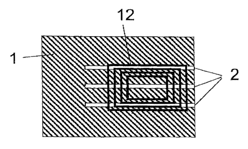
Figure 3 shows the external package 1 with a structure
2 which does not cover the entire length of the
electrically conductive area, but the entire length of
the antenna 12 (the antenna shown here, merely by way
of example and schematically, is a coil for inductive
coupling). The form of the antenna may be quite
different, depending on the field of use; e.g. in the
form of a dipole.
Figure 4 shows a similar design to that in figure 3
with the difference that in this case the structure 2
extends only asfar as at least half of the extent of
the coil 12. In both cases, shielding by the
electrically conductive layer of the external package
is prevented to such an extent that the use of radio
tags is appropriate, that is to say the component is
still operable.
Figure 5 shows an example of a structure which can be
put onto the electrically conductive layer of the
external package 1 over a large area. It is possible to
see a diamond-shaped structure with a large number of
parallel and a large number of nonparallel recesses 7
in which the electrically conductive area 6 of the
electrically conductive layer of the external package 1
is divided into a large number of small areas.
Shielding, which would sensitively disturb the use of
radio tags, is effectively prevented by this means
because small conductive areas bring about no
disturbances in the radio link between the radio tag
and the reader. Particularly if the position of the
coil within the external package is not clear, it makes
sense to put on a large-area structure, as shown here,
because the most effective prevention of shielding is
achieved by a recess in the electrically conductive
area opposite the coil of the electric component, said
coil always being automatically covered too with
application over a large area.
CA 02577901 2007-02-22
- 13 -
Figure 6 shows the shielding area (i.e. the external
package) in the form of a packet 10. An external
transmission antenna 8 is opposite the receiver antenna
11 which is in the packet. On the basis of the prior
art, the electromagnetic radiation between the
transmission antenna 8 and the receiver antenna 11 is
shielded by the packet between them, which has a
conductive area in or on it, so that no radio link is
set up. However, the structure 9 based on the invention
interrupts the conductive area, and it is therefore
possible to set up radio contact between the
transmitter 8 and the receiver 11. The same naturally
also applies if the receiver antenna 11 is not "inside"
the packet but rather on and outside the external
package but in its surroundings.
The structure 9 shown is just one example and, on the
basis of the invention, the structure may naturally
take all possible forms, e.g. including the form shown
in figure 5.
Figure 7 shows a measurement of the shielding effect of
a conductive layer. Between the transmission antenna 8
and the reception antenna 11, a conductive layer,
namely the external package layer 1, is pushed from the
left to the right in the direction of the arrow 18. The
graph at the top now shows the induced voltage measured
at 11 as a function of the overlap by the conductive
layer 1. It can clearly be seen that up to an
approximately 1/3 overlap the induced voltage remains
constant, that is to say there is no shielding effect.
With a larger overlap, a rapid drop in the induced
voltage then occurs, that is to say that a severe
shielding effect occurs. With a complete overlap, it is
almost impossible to measure any induced voltage
(essentially noise), which indicates a largely full
shielding effect. A similar response is also obtained
when the transmitter and receiver antennas are situated
CA 02577901 2007-02-22
/
- 14 -
on one side of the conductive foil and the conductive
foil is passed very close to one of the antennas.
The possibly of reducing the shielding by electrically
conductive external packages, disclosed here for the
first time, allows very simple means and minimum
intervention to be used to reduce the unwanted
shielding effect of conductive areas to magnetic and
electromagnetic fields significantly. It is therefore
possible to accommodate radio tags, for example, within
or in the surroundings of metallized packages without
adversely affecting their operability.
The already publicized intention of many companies to
put RFID tags on a large number of products in future
is also made possible here for products which are
packed in metal foils, metallized and/or metal-
laminated paper or foil and/or composite materials
which contain metal layers.