Note: Descriptions are shown in the official language in which they were submitted.
CA 02578468 2007-02-26
WO 2006/036431 PCT/US2005/030761
MEMS DEVICE HAVING DEFORMABLE MEMBRANE CHARACTERIZED BY
MECHANICAL PERSISTENCE
BACKGROUND
Field of the Invention
[0001] The field of the invention relates to microelectromechanical systems
(MEMS).
Description of the Related Art
[0002] Microelectromechanical systems (MEMS) include micro mechanical
elements,
actuators, and electronics. Micromechanical elements may be created using
deposition, etching,
and or other micromachining processes that etch away parts of substrates
and/or deposited material
layers or that add layers to form electrical and electromechanical devices.
One type of MEMS
device is called an interferometric modulator. As used herein, the term
interferometric modulator
or interferometric light modulator refers to a device that selectively absorbs
and/or reflects light
using the principles of optical interference. In certain embodiments, an
interferometric modulator
may comprise a pair of conductive plates, one or both of which may be
transparent and/or
reflective in whole or part and capable of relative motion upon application of
an appropriate
electrical signal. In a particular embodiment, one plate may comprise a
stationary layer deposited
on a substrate and the other plate may comprise a metallic membrane separated
from the stationary
layer by an air gap. As described herein in more detail, the position of one
plate in relation to
another can change the optical interference of light incident on the
interferometric modulator.
Such devices have a wide range of applications, and it would be beneficial in
the art to utilize
and/or modify the characteristics of these types of devices so that their
features can be exploited in
improving existing products and creating new products that have not yet been
developed.
SUMMARY
[0003] The system, method, and devices of the invention each have several
aspects, no
single one of which is solely responsible for its desirable attributes.
Without limiting the scope of
this invention, its more prominent features will now be discussed briefly.
After considering this
discussion, and particularly after reading the section entitled "Detailed
Description of Certain
Embodiments" one will understand how the features of this invention provide
advantages over
other display devices.
CA 02578468 2007-02-26
WO 2006/036431 PCT/US2005/030761
[0005] In an embodiment, a MEMS device comprises a substrate and a first
layer.
The first layer and the substrate are configured to have a first cavity
therebetween. The first cavity
has a first pressure. The first layer is movable with respect to the substrate
in response to a voltage
applied to at least the first layer. The MEMS device further comprises a
second layer, with the
second layer and the first layer configured to have a second cavity
therebetween. The second
cavity has a second pressure. The MEMS device further comprises a structure in
fluid
communication with at least one of the first and second cavities. The
structure is configured to
manipulate at least one of the first and second pressures to alter a speed of
motion of the first layer.
[0004] In another embodiment, a MEMS device comprises a substrate. The MEMS
device further comprises a first layer comprising at least one aperture. The
first layer and the
substrate are configured to have a first cavity therebetween. The first layer
is movable with respect
to the substrate in response to a voltage applied to at least the first layer.
The MEMS device
further comprises a second layer comprising at least one aperture. The second
layer and the first
layer are configured to have a second cavity therebetween. The first and
second cavities are in
fluid communication through the at least one aperture of the first layer.
[0005] In another embodiment, a method manufactures a MEMS device. The method
comprises providing a substrate. The method further comprises providing a
first sacrificial layer.
The method further comprises forming a first layer comprising at least one
aperture. The first
sacrificial layer is disposed between the substrate and the first layer. The
method further comprises
providing a second sacrificial layer. The first layer is disposed between the
first sacrificial layer
and the second sacrificial layer. The method further comprises forming a
second layer comprising
at least one aperture. The second sacrificial layer is disposed between the
second layer and the first
layer.
[0006] In another embodiment, a method operates a MEMS device. The method
comprises providing a MEMS device comprising a substrate and a first layer.
The first layer and
the substrate have a first cavity therebetween. The first cavity has a first
pressure. The first layer
is movable with respect to the substrate in response to a voltage applied to
at least the first layer.
The MEMS device further comprises a second layer. The second layer and the
first layer have a
second cavity therebetween. The second cavity has a second pressure. The MEMS
device further
comprises a structure in fluid communication with at least one of the first
and second cavities. The
structure is configured to manipulate at least one of the first and second
pressures. The method
further comprises manipulating at least one of the first and second pressures
using the structure.
[0007] In another embodiment, a MEMS device comprises means for supporting a
MEMS device. The MEMS device further comprises means for reflecting light. The
supporting
means and the reflecting means have a first cavity therebetween. The first
cavity has a first
pressure. The reflecting means is movable with respect to the supporting
means. The MEMS
-2-
CA 02578468 2007-02-26
WO 2006/036431 PCT/US2005/030761
device further comprises means for bounding at least a portion of a second
cavity. The second
cavity is located between the reflecting means and the bounding means. The
second cavity has a
second pressure. The MEMS device further comprises means for manipulating at
least one of the
first and second pressures.
[0008] In another embodiment, a MEMS device comprises means for supporting a
MEMS device. The MEMS device further comprises means for conducting
electricity. The
conducting means comprises at least one aperture. The conducting means is
movable with respect
to the supporting means in response to a voltage applied to at least the
conducting means. The
supporting means and the conducting means have a first cavity therebetween.
The MEMS device
further comprises means for dampening movement of the conducting means. The
dampening
means comprises at least one aperture. The conducting means and the dampening
means have a
second cavity therebetween.
[0009] In another embodiment, a MEMS device comprises means for supporting a
MEMS device. The MEMS device further comprises means for conducting
electricity. The
conducting means comprises at least one aperture. The supporting means and the
conducting
means have a first cavity therebetween. The conducting means is movable with
respect to the
supporting means in response to a voltage applied to at least the conducting
means. The MEMS
device further comprises means for bounding at least a portion of a second
cavity. The bounding
means comprises at least one aperture. The bounding means and the conducting
means have a
second cavity therebetween. The first and second cavities are in fluid
communication through the
at least one aperture of the conducting means.
BRIEF DESCRIPTION OF THE DRAWINGS
[0010] Figure 1 is an isometric view depicting a portion of one embodiment of
an
interferometric modulator display in which a movable reflective layer of a
first interferometric
modulator is in a relaxed position and a movable reflective layer of a second
interferometric
modulator is in an actuated position.
[0011] Figure 2 is a system block diagram illustrating one embodiment of an
electronic device incorporating a 3x3 interferometric modulator display.
[0012] Figure 3 is a diagram of movable mirror position versus applied voltage
for
one exemplary embodiment of an interferometric modulator of Figure 1.
[0013] Figure 4 is an illustration of a set of row and column voltages that
may be
used to drive an interferometric modulator display.
[0014] Figure 5A illustrates one exemplary frame of display data in the 3x3
interferometric modulator display of Figure 2.
[0015] Figure 5B illustrates one exemplary timing diagram for row and column
signals that may be used to write the frame of Figure 5A.
-3-
CA 02578468 2007-02-26
WO 2006/036431 PCT/US2005/030761
100161 Figures 6A and 6B are system block diagrams illustrating an embodiment
of a
visual display device comprising a plurality of interferometric modulators.
[0017] Figure 7A is a cross section of the device of Figure 1.
[0018] Figure 7B is a cross section of an alternative embodiment of an
interferometric modulator.
[0019] Figure 7C is a cross section of another alternative embodiment of an
interferometric modulator.
[0020] Figure 7D is a cross section of yet another alternative embodiment of
an
interferometric modulator.
[0021] Figure 7E is a cross section of an additional alternative embodiment of
an
interferometric modulator.
[0022] Figures 8A, 8B, and 8C illustrate geometric variations in the movable
reflective layer that affect the actuation and release times of the modulator
so as to improve the
operational response of the modulator.
[0023] Figure 9 is a partial perspective view of a modulator that includes
holes in the
movable layer.
100241 Figure 10A is a cross sectional view of a modulator that includes holes
in the
movable layer and additionally includes an upper air flow control layer
(otherwise called a
dampening layer) that can function to increase the mechanical persistence of
the actuated state.
[0025] Figure lOB is a cross sectional view of the modulator of Figure l0A
additionally including a structure configured to control one or more pressures
in the modulator.
100261 Figure lOC is a cross sectional view of a modulator that includes holes
in one
or more structural supports or posts of the modulator.
[0027] Figures 11A and 11B are flow charts illustrating an exemplary
fabrication
process for fabricating at least a portion of an interferometric modulator.
[0028] Figure 12A is a plan view of a partially fabricated interferometric
modulator
using the fabrication process embodiment of Figures 11A and 11B.
[0029] Figure 12B is a cross sectional view of the modulator of Figure 12A
taken
along line 12B-12B.
[0030] Figure 13A is a plan view of a partially fabricated interferometric
modulator
using the fabrication process embodiment of Figures 11A and 11B.
[0031] Figure 13B is a cross sectional view of the modulator of Figure 13A
taken
along line 13B-13B.
[0032] Figure 14A illustrates a plan view of a partially fabricated
interferometric
modulator using the fabrication process embodiment of Figures 11A and 11B.
-4-
CA 02578468 2007-02-26
WO 2006/036431 PCT/US2005/030761
[0033] Figures 14B and 14C illustrate cross sectional views of the partially
fabricated
interferometric modulator of Figure 14A taken along lines 14B-14B and 14C-14C
respectively.
DETAILED DESCRIPTION OF THE PREFERRED EMBODIMENTS
[0034] The following detailed description is directed to certain specific
embodiments
of the invention. However, the invention can be embodied in a multitude of
different ways. In this
description, reference is made to the drawings wherein like parts are
designated with like numerals
throughout. As will be apparent from the following description, the
embodiments may be
implemented in any device that is configured to display an image, whether in
motion (e.g., video)
or stationary (e.g., still image), and whether textual or pictorial. More
particularly, it is
contemplated that the embodiments may be implemented in or associated with a
variety of
electronic devices such as, but not limited to, mobile telephones, wireless
devices, personal data
assistants (PDAs), hand-held or portable computers, GPS receivers/navigators,
cameras, MP3
players, camcorders, game consoles, wrist watches, clocks, calculators,
television monitors, flat
panel displays, computer monitors, auto displays (e.g., odometer display,
etc.), cockpit controls
and/or displays, display of camera views (e.g., display of a rear view camera
in a vehicle),
electronic photographs, electronic billboards or signs, projectors,
architectural structures,
packaging, and aesthetic structures (e.g., display of images on a piece of
jewelry). MEMS devices
of similar structure to those described herein can also be used in non-display
applications such as
in electronic switching devices.
[0035] A deformable mechanical membrane (or layer) useful to form a display
device
is provided, wherein the membrane has a faster deformation time constant on
actuation than
relaxation time constant upon release from actuation. This improves the
mechanical persistence of
the actuated state of the membrane, which is desirable in some display
embodiments. In some
embodiments, apertures are formed in the membrane to decrease pressure,
including liquid and/or
gas pressures, on the membrane when actuated. In other embodiments, a
dampening layer is
disposed in close proximity to the membrane to apply greater pressure on the
membrane in the
direction towards the actuated position, thereby slowing the motion of the
membrane when
released from an actuated state. Other embodiments comprise structures, such
as a heating element
or vacuum device, to manipulate pressures above and/or below the mechanical
membrane to affect
the mechanical persistence of the display device. In an exemplary embodiment,
a mechanical
membrane is disposed between a back plate and a substrate. In some
embodiments, the term
"below" refers to the direction from the mechanical membrane towards the
substrate and the term
"above" refers to the direction from the mechanical membrane towards the back
plate. Also, in
some embodiments, a direction towards the actuated position is the same as a
direction from the
mechanical membrane towards the substrate and a direction towards the released
position is the
same as a direction from the mechanical membrane towards the back plate.
-5-
CA 02578468 2007-02-26
WO 2006/036431 PCT/US2005/030761
[0036] As used herein, the term layer is to be given its broadest ordinary
meaning.
Moreover, a layer may comprise several additional sublayers and is not limited
to homogeneous
substances of a thin uniform thickness. Although many of the layers are
depicted as having a
relatively thin sheetlike expanse or region lying over or under another, a
layer as used herein may
comprise a shorter expanse or region or multiple expanses or regions.
[0037] One interferometric modulator display embodiment comprising an
interferometric MEMS display element is illustrated in Figure 1. In these
devices, the pixels are
in either a bright or dark state. In the bright ("on" or "open") state, the
display element reflects a
large portion of incident visible light to a user. When in the dark ("off' or
"closed") state, the
display element reflects little incident visible light to the user. Depending
on the embodiment, the
light reflectance properties of the "on" and "off' states may be reversed.
MEMS pixels can be
configured to reflect predominantly at selected colors, allowing for a color
display in addition to
black and white.
[0038] Figure 1 is an isometric view depicting two adjacent pixels in a series
of
pixels of a visual display, wherein each pixel comprises a MEMS
interferometric modulator. In
some embodiments, an interferometric modulator display comprises a row/column
array of these
interferometric modulators. Each interferometric modulator includes a pair of
reflective layers
positioned at a variable and controllable distance from each other to form a
resonant optical cavity
with at least one variable dimension. In one embodiment, one of the reflective
layers may be
moved between two positions. In the first position, referred to herein as the
relaxed position, the
movable reflective layer is positioned at a relatively large distance from a
fixed partially reflective
layer. In the second position, referred to herein as the actuated position,
the movable reflective
layer is positioned more closely adjacent to the partially reflective layer.
Incident light that reflects
from the two layers interferes constructively or destructively depending on
the position of the
movable reflective layer, producing either an overall reflective or non-
reflective state for each
pixel.
[0039] The depicted portion of the pixel array in Figure 1 includes two
adjacent
interferometric modulators 12a and 12b. In the interferometric modulator 12a
on the left, a
movable reflective layer 14a is illustrated in a relaxed position at a
predetermined distance from an
optical stack 16a, which includes a partially reflective layer. In the
interferometric modulator 12b
on the right, the movable reflective layer 14b is illustrated in an actuated
position adjacent to the
optical stack 16b.
[0040] The optical stacks 16a and 16b (collectively referred to as optical
stack 16), as
referenced herein, typically comprise of several fused layers, which can
include an electrode layer,
such as indium tin oxide (ITO), a partially reflective layer, such as
chromium, and a transparent
dielectric. The optical stack 16 is thus electrically conductive, partially
transparent and partially
-6-
CA 02578468 2007-02-26
WO 2006/036431 PCT/US2005/030761
reflective, and may be fabricated, for example, by depositing one or more of
the above layers onto
a transparent substrate 20. In some embodiments, the layers are patterned into
parallel strips, and
may form row electrodes in a display device as described further below. The
movable reflective
layers 14a, 14b may be formed as a series of parallel strips of a deposited
metal layer or layers
(orthogonal to the row electrodes of 16a, 16b) deposited on top of posts 18
and an intervening
sacrificial material deposited between the posts 18. When the sacrificial
material is etched away,
the movable reflective layers 14a, 14b are separated from the optical stacks
16a, 16b by a defined
gap 19. A highly conductive and reflective material such as aluminum may be
used for the
reflective layers 14, and these strips may form column electrodes in a display
device.
[0041] With no applied voltage, the cavity 19 remains between the movable
reflective
layer 14a and optical stack 16a, with the movable reflective layer 14a in a
mechanically relaxed
state, as illustrated by the pixel 12a in Figure 1. However, when a potential
difference is applied
to a selected row and column, the capacitor formed at the intersection of the
row and column
electrodes at the corresponding pixel becomes charged, and electrostatic
forces pull the electrodes
together. If the voltage is high enough, the movable reflective layer 14 is
deformed and is forced
against the optical stack 16. A dielectric layer (not illustrated in this
Figure) within the optical
stack 16 may prevent shorting and control the separation distance between
layers 14 and 16, as
illustrated by pixel 12b on the right in Figure 1. The behavior is the same
regardless of the
polarity of the applied potential difference. In this way, row/column
actuation that can control the
reflective vs. non-reflective pixel states is analogous in many ways to that
used in conventional
LCD and other display technologies.
[0042] Figures 2 through 5B illustrate one exemplary process and system for
using an
array of interferometric modulators in a display application.
[0043] Figure 2 is a system block diagram illustrating one embodiment of an
electronic device that may incorporate aspects of the invention. In the
exemplary embodiment, the
electronic device includes a processor 21 which may be any general purpose
single- or multi-chip
microprocessor such as an ARM, Pentium , Pentium II , Pentium III , Pentium N
, Pentium
Pro, an 8051, a MIPS , a Power PC , an ALPHA , or any special purpose
microprocessor such
as a digital signal processor, microcontroller, or a programmable gate array.
As is conventional in
the art, the processor 21 may be configured to execute one or more software
modules. In addition
to executing an operating system, the processor may be configured to execute
one or more software
applications, including a web browser, a telephone application, an email
program, or any other
software application.
[0044] In one embodiment, the processor 21 is also configured to communicate
with
an array driver 22. In one embodiment, the array driver 22 includes a row
driver circuit 24 and a
column driver circuit 26 that provide signals to a panel or display array
(display) 30. The cross
-7-
CA 02578468 2007-02-26
WO 2006/036431 PCT/US2005/030761
section of the array illustrated in Figure 1 is shown by the lines 1-1 in
Figure 2. For MEMS
interferometric modulators, the row/column actuation protocol may take
advantage of a hysteresis
property of these devices illustrated in Figure 3. It may require, for
example, a 10 volt potential
difference to cause a movable layer to deform from the relaxed state to the
actuated state.
However, when the voltage is reduced from that value, the movable layer
maintains its state as the
voltage drops back below 10 volts. In the exemplary embodiment of Figure 3,
the movable layer
does not relax completely until the voltage drops below 2 volts. There is thus
a range of voltage,
about 3 to 7 V in the example illustrated in Figure 3, where there exists a
window of applied
voltage within which the device is stable in either the relaxed or actuated
state. This is referred to
herein as the "hysteresis window" or "stability window." For a display array
having the hysteresis
characteristics of Figure 3, the row/colunun actuation protocol can be
designed such that during
row strobing, pixels in the strobed row that are to be actuated are exposed to
a voltage difference of
about 10 volts, and pixels that are to be relaxed are exposed to a voltage
difference of close to zero
volts. After the strobe, the pixels are exposed to a steady state voltage
difference of about 5 volts
such that they remain in whatever state the row strobe put them in. After
being written, each pixel
sees a potential difference within the "stability window" of 3-7 volts in this
example. This feature
makes the pixel design illustrated in Figure 1 stable under the same applied
voltage conditions in
either an actuated or relaxed pre-existing state. Since each pixel of the
interferometric modulator,
whether in the actuated or relaxed state, is essentially a capacitor formed by
the fixed and moving
reflective layers, this stable state can be held at a voltage within the
hysteresis window with almost
no power dissipation. Essentially no current flows into the pixel if the
applied potential is fixed.
[0045] In typical applications, a display frame may be created by asserting
the set of
column electrodes in accordance with the desired set of actuated pixels in the
first row. A row
pulse is then applied to the row I electrode, actuating the pixels
corresponding to the asserted
column lines. The asserted set of column electrodes is then changed to
correspond to the desired
set of actuated pixels in the second row. A pulse is then applied to the row 2
electrode, actuating
the appropriate pixels in row 2 in accordance with the asserted column
electrodes. The row 1
pixels are unaffected by the row 2 pulse, and remain in the state they were
set to during the row 1
pulse. This may be repeated for the entire series of rows in a sequential
fashion to produce the
frame. Generally, the frames are refreshed and/or updated with new display
data by continually
repeating this process at some desired number of frames per second. A wide
variety of protocols
for driving row and column electrodes of pixel arrays to produce display
frames are also well
known and may be used in conjunction with the present invention.
[0046] Figures 4, 5A and 5B illustrate one possible actuation protocol for
creating a
display frame on the 3x3 array of Figure 2. Figure 4 illustrates a possible
set of column and row
voltage levels that may be used for pixels exhibiting the hysteresis curves of
Figure 3. In the
-8-
CA 02578468 2007-02-26
WO 2006/036431 PCT/US2005/030761
Figure 4 embodiment, actuating a pixel involves setting the appropriate column
to -Vbias, and the
appropriate row to +OV, which may correspond to -5 volts and +5 volts
respectively Relaxing the
pixel is accomplished by setting the appropriate column to +Vbias, and the
appropriate row to the
same +OV, producing a zero volt potential difference across the pixel. In
those rows where the row
voltage is held at zero volts, the pixels are stable in whatever state they
were originally in,
regardless of whether the column is at +Vbias, or -Vbias. As is also
illustrated in Figure 4, it will
be appreciated that voltages of opposite polarity than those described above
can be used, e.g.,
actuating a pixel can involve setting the appropriate column to +Vbias, and
the appropriate row to
-OV. In this embodiment, releasing the pixel is accomplished by setting the
appropriate column to
-Vbias, and the appropriate row to the same -OV, producing a zero volt
potential difference across
the pixel.
[0047] Figure 5B is a timing diagram showing a series of row and column
signals
applied to the 3x3 array of Figure 2 which will result in the display
arrangement illustrated in
Figure 5A, where actuated pixels are non-reflective. Prior to writing the
frame illustrated in
Figure 5A, the pixels can be in any state, and in this example, all the rows
are at 0 volts, and all the
columns are at +5 volts. With these applied voltages, all pixels are stable in
their existing actuated
or relaxed states.
[0048] In the Figure 5A frame, pixels (1, 1), (1, 2), (2, 2), (3, 2) and (3,
3) are
actuated. To accomplish this, during a "line time" for row 1, columns 1 and 2
are set to -5 volts,
and column 3 is set to +5 volts. This does not change the state of any pixels,
because all the pixels
remain in the 3-7 volt stability window. Row 1 is then strobed with a pulse
that goes from 0, up to
volts, and back to zero. This actuates the (1, 1) and (1, 2) pixels and
relaxes the (1, 3) pixel. No
other pixels in the array are affected. To set row 2 as desired, column 2 is
set to -5 volts, and
columns 1 and 3 are set to +5 volts. The same strobe applied to row 2 will
then actuate pixel (2, 2)
and relax pixels (2, 1) and (2, 3). Again, no other pixels of the array are
affected. Row 3 is
similarly set by setting columns 2 and 3 to -5 volts, and column 1 to +5
volts. The row 3 strobe
sets the row 3 pixels as shown in Figure 5A. After writing the frame, the row
potentials are zero,
and the column potentials can remain at either +5 or -5 volts, and the display
is then stable in the
arrangement of Figure 5A. It will be appreciated that the same procedure can
be employed for
arrays of dozens or hundreds of rows and columns. It will also be appreciated
that the timing,
sequence, and levels of voltages used to perform row and column actuation can
be varied widely
within the general principles outlined above, and the above example is
exemplary only, and any
actuation voltage method can be used with the systems and methods described
herein.
[0049] Figures 6A and 6B are system block diagrams illustrating an embodiment
of a
display device 40. The display device 40 can be, for example, a cellular or
mobile telephone.
-9-
CA 02578468 2007-02-26
WO 2006/036431 PCT/US2005/030761
However, the same components of display device 40 or slight variations thereof
are also illustrative
of various types of display devices such as televisions and portable media
players.
[0050] The display device 40 includes a housing 41, a display 30, an antenna
43, a
speaker 45, an input device 48, and a microphone 46. The housing 41 is
generally formed from any
of a variety of manufacturing processes as are well known to those of skill in
the art, including
injection molding, and vacuum forming. In addition, the housing 41 may be made
from any of a
variety of materials, including but not limited to plastic, metal, glass,
rubber, and ceramic, or a
combination thereof. In one embodiment the housing 41 includes removable
portions (not shown)
that may be interchanged with other removable portions of different color, or
containing different
logos, pictures, or symbols.
[0051] The display 30 of exemplary display device 40 may be any of a variety
of
displays, including a bi-stable display, as described herein. In other
embodiments, the display 30
includes a flat-panel display, such as plasma, EL, OLED, STN LCD, or TFT LCD
as described
above, or a non-flat-panel display, such as a CRT or other tube device, as is
well known to those of
skill in the art. However, for purposes of describing the present embodiment,
the display 30
includes an interferometric modulator display, as described herein.
[0052] The components of one embodiment of exemplary display device 40 are
schematically illustrated in Figure 6B. The illustrated exemplary display
device 40 includes a
housing 41 and can include additional components at least partially enclosed
therein. For example,
in one embodiment, the exemplary display device 40 includes a network
interface 27 that includes
an antenna 43 which is coupled to a transceiver 47. The transceiver 47 is
connected to the
processor 21, which is connected to conditioning hardware 52. The conditioning
hardware 52 may
be configured to condition a signal (e.g. filter a signal). The conditioning
hardware 52 is connected
to a speaker 45 and a microphone 46. The processor 21 is also connected to an
input device 48 and
a driver controller 29. The driver controller 29 is coupled to a frame buffer
28 and to the array
driver 22, which in turn is coupled to a display array 30. A power supply 50
provides power to all
components as required by the particular exemplary display device 40 design.
[0053] The network interface 27 includes the antenna 43 and the transceiver 47
so that
the exemplary display device 40 can communicate with one ore more devices over
a network. In
one embodiment the network interface 27 may also have some processing
capabilities to relieve
requirements of the processor 21. The antenna 43 is any antenna known to those
of skill in the art
for transmitting and receiving signals. In one embodiment, the antenna
transmits and receives RF
signals according to the IEEE 802.11 standard, including IEEE 802.11(a), (b),
or (g). In another
embodiment, the antenna transmits and receives RF signals according to the
BLUETOOTH
standard. In the case of a cellular telephone, the antenna is designed to
receive CDMA, GSM,
AMPS or other known signals that are used to communicate within a wireless
cell phone network.
-10-
CA 02578468 2007-02-26
WO 2006/036431 PCT/US2005/030761
The transceiver 47 pre-processes the signals received from the antenna 43 so
that they may be
received by and further manipulated by the processor 21. The transceiver 47
also processes signals
received from the processor 21 so that they may be transmitted from the
exemplary display device
40 via the antenna 43.
[00541 In an alternative embodiment, the transceiver 47 can be replaced by a
receiver.
In yet another alternative embodiment, network interface 27 can be replaced by
an image source,
which can store or generate image data to be sent to the processor 21. For
example, the image
source can be a digital video disc (DVD) or a hard-disc drive that contains
image data, or a
software module that generates image data.
[0055] Processor 21 generally controls the overall operation of the exemplary
display
device 40. The processor 21 receives data, such as compressed image data from
the network
interface 27 or an image source, and processes the data into raw image data or
into a format that is
readily processed into raw image data. The processor 21 then sends the
processed data to the
driver controller 29 or to frame buffer 28 for storage. Raw data typically
refers to the information
that identifies the image characteristics at each location within an image.
For example, such image
characteristics can include color, saturation, and gray-scale level.
[0056] In one embodiment, the processor 21 includes a microcontroller, CPU, or
logic
unit to control operation of the exemplary display device 40. Conditioning
hardware 52 generally
includes amplifiers and filters for transmitting signals to the speaker 45,
and for receiving signals
from the microphone 46. Conditioning hardware 52 may be discrete components
within the
exemplary display device 40, or may be incorporated within the processor 21 or
other components.
[0057] The driver controller 29 takes the raw image data generated by the
processor
21 either directly from the processor 21 or from the frame buffer 28 and
reformats the raw image
data appropriately for high speed transmission to the array driver 22.
Specifically, the driver
controller 29 reformats the raw image data into a data flow having a raster-
like format, such that it
has a time order suitable for scanning across the display array 30. Then the
driver controller 29
sends the formatted information to the array driver 22. Although a driver
controller 29, such as a
LCD controller, is often associated with the system processor 21 as a stand-
alone Integrated Circuit
(IC), such controllers may be implemented in many ways. They may be embedded
in the processor
21 as hardware, embedded in the processor 21 as software, or fully integrated
in hardware with the
array driver 22.
[0058] Typically, the array driver 22 receives the formatted information from
the
driver controller 29 and reformats the video data into a parallel set of
waveforms that are applied
many times per second to the hundreds and sometimes thousands of leads coming
from the
display's x-y matrix of pixels.
-11-
CA 02578468 2007-02-26
WO 2006/036431 PCT/US2005/030761
[0059] In one embodiment, the driver controller 29, array driver 22, and
display array
30 are appropriate for any of the types of displays described herein. For
example, in one
embodiment, driver controller 29 is a conventional display controller or a bi-
stable display
controller (e.g., an interferometric modulator controller). In another
embodiment, array driver 22 is
a conventional driver or a bi-stable display driver (e.g., an interferometric
modulator display). In
one embodiment, a driver controller 29 is integrated with the array driver 22.
Such an embodiment
is common in highly integrated systems such as cellular phones, watches, and
other small area
displays. In yet another embodiment, display array 30 is a typical display
array or a bi-stable
display array (e.g., a display including an array of interferometric
modulators).
[0060] The input device 48 allows a user to control the operation of the
exemplary
display device 40. In one embodiment, input device 48 includes a keypad, such
as a QWERTY
keyboard or a telephone keypad, a button, a switch, a touch-sensitive screen,
a pressure- or heat-
sensitive membrane. In one embodiment, the microphone 46 is an input device
for the exemplary
display device 40. When the microphone 46 is used to input data to the device,
voice commands
may be provided by a user for controlling operations of the exemplary display
device 40.
[0061] Power supply 50 can include a variety of energy storage devices as are
well
known in the art. For example, in one embodiment, power supply 50 is a
rechargeable battery,
such as a nickel-cadmium battery or a lithium ion battery. In another
embodiment, power supply
50 is a renewable energy source, a capacitor, or a solar cell, including a
plastic solar cell, and solar-
cell paint. In another embodiment, power supply 50 is configured to receive
power from a wall
outlet.
[0062] In some implementations control programmability resides, as described
above,
in a driver controller which can be located in several places in the
electronic display system. In
some cases control programmability resides in the array driver 22. Those of
skill in the art will
recognize that the above-described optimization may be implemented in any
number of hardware
and/or software components and in various configurations.
[0063] The details of the structure of interferometric modulators that operate
in
accordance with the principles set forth above may vary widely. For example,
Figures 7A-7E
illustrate five different embodiments of the movable reflective layer 14 and
its supporting
structures, wherein each embodiment comprises a modulator cavity 19. Figure 7A
is a cross
section of the embodiment of Figure 1, where a strip of metal material 14 is
deposited on
orthogonally extending supports 18. In Figure 7B, the moveable reflective
layer 14 is attached to
supports at the corners only, on tethers 32. In Figure 7C, the moveable
reflective layer 14 is
suspended from a deformable layer 34, which may comprise a flexible metal. The
deformable
layer 34 connects, directly or indirectly, to the substrate 20 around the
perimeter of the deformable
layer 34. These connections are herein referred to as support posts. The
embodiment illustrated in
-12-
CA 02578468 2007-02-26
WO 2006/036431 PCT/US2005/030761
Figure 7D has support post plugs 42 upon which the deformable layer 34 rests.
The movable
reflective layer 14 remains suspended over the cavity, as in Figures 7A-7C,
but the deformable
layer 34 does not form the support posts by filling holes between the
deformable layer 34 and the
optical stack 16. Rather, the support posts are formed of a planarization
material, which is used to
form support post plugs 42. The embodiment illustrated in Figure 7E is based
on the embodiment
shown in Figure 7D, but may also be adapted to work with any of the
embodiments illustrated in
Figures 7A-7C as well as additional embodiments not shown. In the embodiment
shown in Figure
7E, an extra layer of metal or other conductive material has been used to form
a bus structure 44.
This allows signal routing along the back of the interferometric modulators,
eliminating a number
of electrodes that may otherwise have had to be formed on the substrate 20.
[0064] In embodiments such as those shown in Figure 7, the interferometric
modulators function as direct-view devices, in which images are viewed from
the front side of the
transparent substrate 20, the side opposite to that upon which the modulator
is arranged. In these
embodiments, the reflective layer 14 optically shields some portions of the
interferometric
modulator on the side of the reflective layer opposite the substrate 20,
including the deformable
layer 34 and the bus structure 44. This allows the shielded areas to be
configured and operated
upon without negatively affecting the image quality. This separable modulator
architecture allows
the structural design and materials used for the electromechanical aspects and
the optical aspects of
the modulator to be selected and to function independently of each other.
Moreover, the
embodiments shown in Figures 7C-7E have additional benefits deriving from the
decoupling of
the optical properties of the reflective layer 14 from its mechanical
properties, which are carried
out by the deformable layer 34. This allows the structural design and
materials used for the
reflective layer 14 to be optimized with respect to the optical properties,
and the structural design
and materials used for the deformable layer 34 to be optimized with respect to
desired mechanical
properties.
[0065] In some embodiments of display devices made from this modulator design,
it is
desirable for the moveable layer to transition from the unactuated/relaxed
state to the
actuated/deformed state very quickly. At the same time, it can be advantageous
for the opposite
transition back to the relaxed state to occur slowly, even when no voltage is
present across the
electrodes of a given pixel. This can be referred to as mechanical
persistence, whereby the
moveable layer will deform quickly in response to a voltage pulse across the
electrodes, but will
remain in the deformed state for a while after the pulse is over and the
voltage returns to zero. In
some display embodiments, this mechanical persistence makes the formed image
persist for the
time necessary to sequentially actuate all the rows of the display, at which
point a "refresh" can be
performed before the image decays due to relaxation of the individual
modulators. In addition, if a
set of moveable layers in a display are not fully relaxed between image
refresh cycles, a refresh or
-13-
CA 02578468 2007-02-26
WO 2006/036431 PCT/US2005/030761
update can be performed faster and with less energy since the set of moveable
layers are already at
least partially actuated when the refresh/update is performed.
[0066] Stable operation of the MEMS interferometric modulator is achieved by
selecting mechanical design features of the interferometric modulator that
optimize the actuation
and release times for the particular row/colunin actuation protocol. Described
herein are certain
structures and methods of making interferometric modulators having varying
release and actuation
times. In general, the mechanical persistence of the movable layer may be
changed by
manipulating forces acting upon the movable layer, such as a differential gas
pressure, a
differential liquid pressure, or a combination of liquid and gas pressures.
Typically, the pressure
acting upon the movable layer will be from a gas occupying a space above
and/or below the
movable layer. Accordingly, in some embodiments the pressure(s) exerted on the
movable layer is
a gas, such as air. In other embodiments, the gas may be any gas suitable for
use in an
interferometric modulator. In other embodiments, a liquid may occupy the space
above and/or
below the movable layer. Accordingly, in some embodiments the pressure(s)
exerted on the
movable layer is a liquid, such as liquids typically used in LCD displays or
any other liquid
suitable for use in displays. A differential pressure that acts in a direction
towards the actuated
position will decrease actuation time and increase release time. Conversely, a
differential pressure
that acts in a direction towards the opposite of the actuated position will
increase actuation time
and decrease release time.
[0067] Manipulation of the mechanical persistence of the movable layer allows
an
interferometric modulator to be operated without using the hysteresis property
of the modulator
(illustrated in Figures 3 through 5). Instead, the processes and systems
described herein may be
used with row/column actuation protocols which maintain voltages to the MEMS
interferometric
modulators that are above or below the "hysteresis window" or "stability
window." These
protocols may advantageously operate the MEMS interferometric modulator at
lower voltages than
the voltages employed with the processes and systems described with reference
to Figures 3
through 5. Examples of such actuation protocols are described in U.S. Patent
Application No.
11/112,487, entitled "Device and Method for Display Memory Using Manipulation
of Mechanical
Response," filed April 22, 2005, incorporated by reference herein in its
entirety.
[0068] The mechanical persistence of the movable layer may be changed by
manipulating a differential pressure acting upon the movable layer. Such a
differential pressure
may be pressure exerted on the movable layer from gas and/or liquid. A
differential pressure that
acts in a direction of the actuated position will decrease actuation time and
increase release time.
Conversely, a differential pressure that acts in a direction opposite of the
actuated position will
increase actuation time and decrease release time. Figures 8 through 14
illustrate such methods
and structures for manipulating the mechanical persistence of the movable
layer of an
-14-
CA 02578468 2007-02-26
WO 2006/036431 PCT/US2005/030761
interferometric modulator. Although many of the protocols, methods, and
apparatus described
herein reference gas pressures, these same protocols, methods, and apparatus
may be used with
pressure(s) created by liquids or a combination of gas and liquid.
[0069] Figures 8A through 8C illustrate a geometric variation in the movable
layer 14
that affects a gas pressure acting upon the movable layer, thereby affecting
actuation and release
times of the modulator so as to improve the operational response of the
modulator. When the
modulator is actuated and the cavity 19 (depicted in Figure 1 and Figures 7A
through 7E) is
collapsed, gas in the cavity 19, typically air, is forced out of the cavity
19, thereby decreasing a gas
pressure within the cavity 19. By perforating the movable layer 14, the gas is
allowed to pass out
of the cavity 19 through the movable layer 14, resulting in a decrease in the
actuation time. In
Figure 8A a solid movable layer 14 is illustrated. In Figure 8B, the movable
layer 14 includes one
or more perforations 1500 (also referred to as apertures or holes) so as to
decrease the actuation
time of the modulator. This will also increase the release time, however,
because the gas pressure
that would have built up beneath the collapsed movable layer 14 has been
discharged. In other
embodiments, the cavity 19 is filled with a liquid and the one or more
perforations 1500 in the
movable layer 14 similarly function to change the actuation and release time
of the modulator.
[0070] As illustrated in Figure 8C, the perforations 1500 may be located
anywhere on
the movable layer 14, including an edge portion 1500a on a periphery of the
movable layer 14 and
including an inside portion 1500b of the movable layer 14. As used herein, the
terms hole or
perforation are to be given their broadest ordinary meaning. Moreover, the
perforations 1500 (or
holes) may be of any size or pattern, including but not limited to rectangular
and/or circular shapes
that are scattered and/or in an ordered array.
[0071] Figures 9, 10A, lOB, and lOC illustrate embodiments of an
interferometric
modulator that exhibits a relatively high degree of mechanical persistence,
wherein the actuation
time of the modulator is decreased and the release time of the modulator is
increased as compared
to the modulator illustrated in Figures 1 and 7A-E. Referring to Figures 9,
l0A and lOB, an
interferometric modulator 501 includes an array of cavities 498a, 498b, 498c
fabricated on a
substrate 500. As described below, the cavities 498a, 498b, 498c are filled
with a gas, such as air.
However, in other embodiments, the cavities 498a, 498b, 498c may be filled
with a liquid.
[0072] As used herein, the term cavity is to be given its broadest ordinary
meaning,
including but not limited to a space or hollow area that is surrounded by
something such as, but not
limited to, one or more layers or structures. As used herein the term
substrate is to be given its
broadest ordinary meaning, including but not limited to a layer fabricated out
of any material at
least partially transmissive to light, including but not limited to glass and
plastic; the substrate may
also be fabricated into a variety of forms, including but not limited to a
homogeneous substance of
-15-
CA 02578468 2007-02-26
WO 2006/036431 PCT/US2005/030761
a thin uniform thickness, a non-homogenous substance or non-uniform thickness;
the substrate may
also have several sublayers, a shorter expanse or region or multiple expanses
or regions.
[0073] Each cavity 498a, 498b, 498c may be formed by a combination of
dielectric
and metallic materials forming mirrors on two layers. The first layer 502a,
502b, 502c forming the
cavities 498a, 498b, 498c, respectively, is a primary mirror/conductor
comprised of a transparent
conductive coating upon which a dielectric or metallic mirror has been
fabricated. In some
embodiments, layers 502a, 502b, 502c may include a lower layer 502a1, 502b1,
502c1,
respectively, comprised of indium-tin-oxide (also referred to herein as ITO).
In some
embodiments, the layers 502a, 502b, 502c may also include an upper layer
502a2, 502b2, 502c2,
respectively, comprised of chromium. The ITO functions as an optically
transparent electrical
conductor, and the chromium functions as a partial reflector. Insulating
supports 504 hold up the
second layer 506a, 506b, 506c of the cavities 498a, 498b, 498c, respectively.
The second layer
506a, 506b, 506c is also referred to as the movable layer and functions as the
secondary
mirror/conductor. The movable layer 506a, 506b, 506c may comprise aluminum and
is flexible.
The movable layer 506a, 506b, 506c is also fabricated such that it is under
tensile stress and thus
parallel to the substrate 500 in the undriven state.
[0074] As shown in Figures 9, 10A and IOB, the movable layers 506a, 506b, and
506c can include holes 550 in the deforming regions 551a, 551b, 551c,
respectively. These holes
550 reduce a gas pressure acting upon the movable layers 506a, 506b, 506c as
each movable layer
deforms downward through an intervening layer of gas that occupies the
respective cavities 498a,
498b, 498c below the movable layers 506a, 506b, 506c. Without the holes 550,
the gas occupying
cavities 498a, 498b, 498c would exert a pressure on its respective movable
layer 506a, 506b, 506c
as the movable layer deforms downward. With the holes 550, however, the gas
occupying cavities
498a, 498b, 498c is allowed to escape through the holes 550 of the respective
movable layer 506a,
506b, 506c that is deforming towards the substrate 500 resulting in a decrease
of the actuation time.
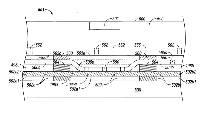
In alternative embodiments, holes 550 may be formed in one or more of the
movable layers 506a,
506b, 506c.
[0075] As shown in Figures 10A and lOB, to slow down the reverse transition
during
release of the movable layer 506a, 506b, 506c, an additional layer of material
555 (also referred to
as a dampening layer) is deposited over an array on short posts 560 that run
perpendicular to the
movable layers 506a, 506b, 506c. The layer 555 may be formed out of a variety
of materials,
including but not limited to metals, dielectric materials, glass, plastic and
polymer materials. The
layer 555 may be spin coated or deposited using general deposition techniques.
The layer 555 may
be any suitable thickness, including but not limited to 1000 angstroms to 10
microns.
[0076] In one embodiment, the layer 555 forms an upper portion of cavities
565a,
565b, 565c, and the movable layers 506a, 506b, 506c form a lower portion of
cavities 565a, 565b,
-16-
CA 02578468 2007-02-26
WO 2006/036431 PCT/US2005/030761
565c. In alternative embodiments, the layer 555 may be disposed above one or
more of the
movable layers 506a, 506b, 506c. The holes 550 in the movable layers 506a,
506b, 506c fluidly
couple the cavities 498a, 498b, 498c below the movable layers with the
cavities 565a, 565b, 565c
above the movable layers. A fluid coupling means, at least, that gas, such as
air, may pass between
the cavities above and below the movable layers 506a, 506b, 506c. In other
embodiments, the
cavities 565a, 565b, 565c may be filled with a liquid.
[0077] In some prior embodiments, the area 565a, 565b, 565c above the movable
layers 506a, 506b, 506c, respectively, was covered with a back plate 600 that
would reside a
relatively large distance away from the movable layers 506a, 506b, 506c. In
the embodiment of
Figures 10A and lOB, the layer 555 is very close to the movable layers 506a,
506b, 506c when the
movable layers are in a relaxed state, as illustrated by movable layers 506b
and 506c. In some
embodiments, the layer 555 is spaced from the unactuated or relaxed movable
layers 506b, 506c by
a distance between 200 to 2000 angstroms, including but not limited to 200,
250, 300, 350, 400,
450, 500, 550, 600, 650, 700, 750, 800, 850, 900, 950, 1000, 1050, 1100, 1150,
1200, 1250, 1300,
1350, 1400, 1450, 1500, 1550, 1600, 1650, 1700, 1750, 1800, 1850, 1900, 1950,
and 2000
angstroms. The distance between the layer 555 and unactuated movable layers
506b, 506c is a
height dimension of the corresponding cavities 565b, 565c. Because of the
close proximity of the
layer 555 and the movable layers 506a, 506b, 506c, the layer 555 traps gas,
such as air, more than
the prior embodiments which include only the more distant back plate 600. It
will be appreciated
that in the embodiments of Figures 9, 10A and l OB, the back plate 600 would
still be utilized, and
would reside over the layer 555 after installation.
[0078] In some embodiments, holes 562 in the layer 555 can be formed. These
holes
562 may be formed proximate to one or more of the movable layers 506a, 506b,
506c. To maintain
the gas and/or liquid flow restriction and gas and/or liquid pressure
manipulation provided in part
by the layer 555, in some embodiments the holes 562 may be formed in positions
that are not
aligned with the holes 550 in the movable layers, such as movable layer 506a.
In other
embodiments, at least a portion or all of the holes 562 and 550 may be
aligned. In embodiments
where the layer 555 has holes 562, the cavities 498a, 498b, 498c below the
movable layers 506a,
506b, 506c are fluidly coupled via the holes 550 with the cavities 565a, 565b,
565c above the
movable layers; the cavities 565a, 565b, 565c above the movable layers are
also in fluid
communication via the holes 562 with a space 590 between the back plate 600
and the layer 555.
Thus, with holes 562 and 550, there is fluid communication between the space
590 and the upper
cavities 565a, 565b, 565c, and the lower cavities 498a, 498b, 498c. The net
result of holes 550,
layer 555, and holes 562 is an increase in the ratio of actuation time to
relaxation time of the
interferometric modulator 501 and the movable layer(s). This improves the
mechanical persistence
-17-
CA 02578468 2007-02-26
WO 2006/036431 PCT/US2005/030761
of the interferometric modulator 501. Accordingly, the holes 550, layer 555,
and holes 562 are
each means for manipulating the pressures within the cavities of the
interferometric modulator 501.
[0079] Referring to Figure lOB, in some embodiments, a structure 591 is formed
in
the interferometric modulator 501, where the structure 591 is configured to
improve the mechanical
persistence of the interferometric modulator 501. As used herein, the term
structure is to be given
its broadest ordinary meaning, including but not limited to any definite
composition.
[0080] The structure 591 is also another means for manipulating the pressures
within
the cavities of the interferometric modulator 501. In some embodiments, the
structure may
manipulate a first gas pressure within the cavities 498a, 498b, 498c below the
movable layers 506a,
506b, 506c, and/or it may manipulate a second gas pressure within the cavities
565a, 565b, 565c
above the movable layers 506a, 506b, 506c. In other embodiments, the structure
591 may
manipulate a first liquid pressure within the cavities 498a, 498b, 498c below
the movable layers
506a, 506b, 506c, and/or it may manipulate a second liquid pressure within the
cavities 565a, 565b,
565c above the movable layers 506a, 506b, 506c. In other embodiments, the
structure may
manipulate a first pressure within the cavities 498a, 498b, 498c below the
movable layers 506a,
506b, 506c, and/or it may manipulate a second pressure within the cavities
565a, 565b, 565c above
the movable layers 506a, 506b, 506c, where the first or second pressure may be
either a gas or
liquid pressure. In one embodiment, the structure 591 is formed in the space
590 above the layer
555. In another embodiment, the structure 591 is formed on the back plate 600.
[0081] The structure 591 can be any device configured to manipulate pressures
within
the cavities of the interferometric modulator 501. In some embodiments, the
structure 591 is a
heating element configured to heat a gas occupying the cavities in fluid
communication with the
structure 591, which may include cavities 565a, 565b, 565c if holes 562 are
present in the layer
555, and may include cavities 498a, 498b, 498c if holes 550 are present in the
movable layers 506a,
506b, 506c. If the holes 562 and 550 are both present, the heating element can
be used to
simultaneously manipulate the gas pressures within the cavities above and
below the movable
layers that are in fluid communication with the heating element 591. As used
herein the term
heating element is to be given its broadest ordinary meaning, including but
not limited to a device
or component that produces heat.
[0082] In some embodiments, the heating element can be located in space 590
and is
configured to heat a gas, such as air, in the space 590 and the cavities that
are in fluid
communication with the space 590. When heated, the pressure of the gas within
the cavities
increases according to the ideal gas law PV = nRT, where P is a pressure of
the gas and T is a
temperature of the gas. Thus, in one embodiment, the heating element may be
used to slow the
release of one or more of the movable layers, such as movable layer 506A. In
this embodiment,
motion of the movable layer 506a is slowed because the heated gas in the
cavity 565a above the
-18-
CA 02578468 2007-02-26
WO 2006/036431 PCT/US2005/030761
movable layer 506a applies an increased pressure on the movable layer 506a in
the direction of the
substrate 500. The pressure from the heated gas is greater than the pressure
that would normally be
applied to the movable layer 506a when the gas is not heated by the heating
element.
[0083] In another embodiment, the heating element can be configured to heat or
cool a
liquid in the space 590 and the cavities that are in fluid communication with
the space 590. When
heated, the viscosity of the liquid within the cavities decreases. Viscosity
is a measure of the
resistance to flow. They become less viscous, therefore, as the temperature
increases. The
viscosity of water, for example, decreases from 1.77 centipoise at 0 C to 0.28
centipoise at 100 C.
Thus, in one embodiment, the heating element may be used to reduce the release
time of one or
more of the movable layers, such as movable layer 506A. In this embodiment,
motion of the
movable layer 506a is increased because the heated liquid in the cavity 565a
above the movable
layer 506a applies a decreased viscosity resistance on the movable layer 506a
in the direction of the
substrate 500 when the movable layer 506a moves through the liquid.
[0084] In other embodiments, the structure 591 is a heating element that is
configured
to both increase the speed of motion of one or more of the movable layers
during actuation of the
movable layer(s) and decrease the speed of motion of the movable layer(s)
during release of the
movable layer(s). In these embodiments, the one or more movable layers, such
as movable layer
506a, does not have apertures 550. Accordingly, the heating element is in
fluid communication
with the cavities 565a, 565b, 565c through holes 562 in the layer 555. The
heating element in
space 590 may then heat a gas, such as air, in the space 590 and the cavities
565a, 565b, 565c that
are in fluid communication with the space 590, thereby increasing the pressure
of the gas and the
force applied above the movable layers 506a, 506b, 506c. Due to the increased
pressure from the
gas pressing on the movable layers in a direction towards the actuated
position, the motion of the
movable layers will be increased during actuation of the movable layers;
likewise, the increased
pressure in a direction towards the opposite the actuated position, the motion
of the movable layers
will be slowed during the release of the movable layers. In other embodiments
where only the gas
pressure pressing the movable layer towards the actuated position is present,
the layer 555 can be
absent. In this embodiment, the post 560 may extend from the movable layer 506
to the back plate
600. The structure 591 could then be used to manipulate the gas pressure in
the space above the
movable element 506, where the space is between the back plate 600 and the
movable layer 506.
[0085] In other embodiments, the structure 591 is a vacuum device configured
to alter
pressures within the cavities of the interferometric modulator 501. As used
herein the term vacuum
device is to be given its broadest ordinary meaning, including but not limited
to a device or
component configured to manipulate a pressure, such as but not limited to a
pump that can remove
or inject gas and /or liquid into one or more spaces or cavities. In these
embodiments, the vacuum
device may be configured and used in a similar manner as the heating element
described above.
-19-
CA 02578468 2007-02-26
WO 2006/036431 PCT/US2005/030761
The vacuum device can be used to increase or decrease the pressure applied to
the movable layers
by changing, for example, a gas pressure within the cavities above and/or
below the movable
layers. For example, in some embodiments, the one or more movable layers, such
as movable layer
506a, does not have apertures 550. Accordingly, the vacuum is in fluid
communication with the
cavities 565a, 565b, 565c through holes 562 in the layer 555. The vacuum
device in space 590 may
then pump gas, such as air, in the space 590 and the cavities 565a, 565b, 565c
that are in fluid
communication with the space 590, thereby increasing the pressure of the gas
and the force applied
above the movable layers 506a, 506b, 506c. When the gas pressure in the cavity
565a is increased
by the vacuum device, the motion of the movable layer 506a will be increased
during actuation and
the motion of the movable layer 506a will be decreased during release.
[00861 In alternative embodiments, one or more of the cavities of the
modulator 501,
such as cavities 565a, 565b, 565c, are filled with liquid and the vacuum
device is configured to
pump liquid into or out of the cavities. In these embodiments, the vacuum
device is configured to
inject or remove liquid within one or more of the cavities surrounding, for
example, the movable
layer 506a of the modulator 501. In some embodiments, the vacuum device may
draw liquid from
or place liquid within a reservoir (not depicted). By manipulating the volume
of liquid within one
or more of the cavities, the vacuum device may increase or decrease the
pressure or force exerted
on the movable layer 506a.
[0087] In various embodiments, the interferometric modulator 501 and the
vacuum
device can be configured such that the vacuum device manipulates pressures
within the cavities
above the movable layers simultaneously or independent of the pressures below
the movable
layers. In some embodiments, the vacuum device is the structure 591 in the
space 590 above the
layer 555. In one such embodiment, one or more of the movable layers, such as
movable layer
506a, does not have apertures 550. Accordingly, the vacuum device is in fluid
communication with
at least the cavity 565a above the movable layer 506a. The vacuum device in
space 590 may then
increase the pressure, such as a gas pressure from air or a liquid pressure,
in the space 590 and the
cavity 565a that is in fluid conununication with the space 590, thereby
increasing the pressure and
the force applied above the movable layer 506a. Due to the increased pressure
pressing down on
the movable layer 506a, the motion of the movable layer 506a will be increased
during actuation
and the motion will slow the release of the movable layer 506a. Because the
holes 550 are not
present in the movable layer 506a, the vacuum device is not in fluid
communication with the cavity
498a below the movable layer 506a. Thus, in this embodiment, the vacuum device
can manipulate
the pressure within the cavity 565a above the movable layer 506a independent
of the pressure in
the cavity 498a below the movable layer 506a.
[0088] In other embodiments, the holes 550 in the movable layers, such as
movable
layer 506a, are present, as well as the holes 562 in the layer 555 above the
movable layer 506a.
-20-
CA 02578468 2007-02-26
WO 2006/036431 PCT/US2005/030761
The vacuum device is therefore in fluid communication with both cavities 565a
and 498a above
and below the movable layer 506a. Accordingly, the vacuum device can be used
to simultaneously
manipulate the pressures within the cavities 565a and 498a above and below the
movable layer
506a since the cavities are both in fluid communication with the vacuum
device.
[0089] Referring to Figure lOC, in alternative embodiments of the
interferometric
modulator depicted in Figures 10A and lOB, one or more of the posts 560
bordering the cavity 565
above the movable layer 506 may be configured with holes 592 and/or one or
more of the posts 504
bordering the cavity 498 below the movable layer 506 may be configured with
holes 593. In these
embodiments, the holes 592 and/or 593 in the posts 560 and/or 504,
respectively, can be used in
conjunction with a structure that is configured to improve the mechanical
persistence of the
interferometric modulator 501. The holes 592 and/or 593 are another means for
manipulating the
pressures, such as a gas pressure from air or a liquid pressure, within the
cavities of the
interferometric modulator 501. In one embodiment, the movable layer 506 and
the layer 555 above
the movable layer 506 do not have holes. Rather, the hole 592 in post 560 is
in fluid
communication with the cavity 565 above the movable layer 506. Using a
structure, such as a
heating element or vacuum device, in fluid communication with the hole 592,
the pressure within
the cavity 565 may be manipulated independent of the pressure within the
cavity 498 below the
movable layer 506. Accordingly, the mechanical persistence of the
interferometric modulator 501
and the movable layer 506 is increased when the pressure within the cavity 565
above the movable
layer 506 is manipulated by the structure via the hole 592 to be greater than
the pressure within the
cavity 498 below the movable layer 506. Moreover, in this embodiment, the
layer 555 above the
movable layer 506 can be absent. In this embodiment, the post 560 may extend
from the movable
layer 506 to the back plate 600. The hole 592 can then be used in conjunction
with a structure,
such as a heating element or vacuum device, to manipulate the pressure in the
space above the
movable element 506, where the space is between the back plate 600 and the
movable layer 506.
[0090] In an alternative embodiment, the hole 593 can be used to manipulate
the
pressure within the cavity 498 similar to the embodiments where hole 592 is
used to manipulate the
pressure within the cavity 565. Using a structure, such as a heating element
or vacuum device, in
fluid communication with the hole 593, the pressure within the cavity 498 may
be manipulated
independent of the pressure within the cavity 592 above the movable layer 506.
Accordingly, the
mechanical persistence of the interferometric modulator 501 and the movable
layer 506 is
increased when the pressure within the cavity 498 below the movable layer 506
is manipulated by
the structure via the hole 593 to be less than the pressure within the cavity
565 above the movable
layer 506. Moreover, as in other embodiments discussed previously, the layer
555 above the
movable layer 506 can be absent since the pressures within the cavities are
manipulated without
need for the layer 555.
-21-
CA 02578468 2007-02-26
WO 2006/036431 PCT/US2005/030761
[0091] In other embodiments, the holes 592 and 593 are both present in posts
560 and
504, respectively, such that the pressures within the separate cavities 565
and 498 may be
controlled simultaneously and/or independently. In these embodiments, there
can be separate
structures, such as a heating element or vacuum device, in fluid communication
with each of the
holes 592 and 593. With a separate structure in fluid communication with each
hole(s) 592 and
593, the cavities 565 and 498 may be manipulated to have different pressures.
Moreover, in some
embodiments, the structure(s) in fluid communication with the hole(s), such as
holes 592 and/or
593, may be located at an end of a row of interferometric modulators 501.
Thus, a single structure
in fluid communication with the hole(s) 592 and/or 593 can manipulate the
pressures within the
respective cavities of an entire row of an array of interferometric modulators
501, as long as the
cavities lined up in the row are in fluid communication with one another
through the holes in the
post(s) 560 and/or 593 of each interferometric modulator 501.
[0092] The structure, layers, and holes in the layers and posts of the
interferometric
modulator 501, such as layers 502a, 502b, 502c, posts 504, layer 555, layers
506a, 506b, 506c,
posts 560, posts 504, holes 562, holes 550, holes 592, or holes 593 can be
fabricated using
semiconductor manufacturing techniques, such as photolithography, deposition
(e.g., "dry"
methods such as chemical vapor deposition (CVD) and wet methods such as spin
coating),
masking, shadow masking, lift-off processing, and etching (e.g., dry methods
such as plasma etch
and wet methods). Examples of suitable techniques are described in U.S. Pat.
No. 6,040,937, filed
on Jul. 31, 1996, and U.S. Patent 5,835,255, filed May 5, 1994, both of which
are incorporated
herein in their entirety.
[0093] In some embodiments, the cavities 498a, 498b, 498c are produced by
first
fabricating a solid set of layers 502a, 502b, 502c, 506a, 506b, 506c, 555
where the cavity areas
498a, 498b, 498c, 565a, 565b, 565c are filled with a sacrificial layer of
material such as
molybdenum. The thickness of the sacrificial layer is typically selected by
taking into
consideration the desired color of the modulator in the unactuated position,
and by taking into
consideration the fabrication process (e.g., dry etch) used to remove the
sacrificial layer. In a
preferred embodiment, the thickness of the sacrificial layer is in the range
of about 400 angstroms
to about 6,000 angstroms. For example, in the illustrated embodiment, the
sacrificial layer has a
thickness of about 2,000 angstroms. An artisan will recognize from the
disclosure herein that the
sacrificial layer may include, in addition to or instead of molybdenum, one or
more other readily
removable materials such as silicon (Si), titanium (Ti), tungsten (W), and
germanium (G).
100941 After all the layers 502a, 502b, 502c, 506a, 506b, 506c, 555 are
deposited, the
sacrificial material is removed with a dry etch by exposing the layers to an
etch gas. To fabricate
the device of Figures 9, l0A and lOB, the upper cavities 565a, 565b, 565c are
also formed with
sacrificial material between the posts 560 during the initial solid state
fabrication process. The
-22-
CA 02578468 2007-02-26
WO 2006/036431 PCT/US2005/030761
layer 555 is then fabricated with the holes 562 in order to allow the dry etch
gas to contact the
sacrificial material originally deposited in cavity areas 565a, 565b, 565c and
then down to lower
cavities 498a, 498b, 498c.
[0095] In other embodiments, a lift-off processing technique is preferably
used to
form portions of the interferometric modulator, including but not limited to
the layers with
apertures, such as layers 506a and 555 having apertures 550 and 562
respectively, and/or posts 560
and 504 having holes 592 and 593 respectively. The lift-off is disclosed in
U.S. Application No.
11/155,379, entitled "Method of Fabricating Interferometric Devices Using Lift-
Off Processing
Techniques," filed June 17, 2005, incorporated herein in its entirety. The
term "lift-off processing"
includes its broad ordinary and customary meaning, including fabrication
processes resulting in the
definition of a pattern on a substrate surface (without requiring etching of
the material to remain in
the product), as may be generally used to pattern geometry of hard-to-etch
metals such as gold. In
lift-off processing, materials are deposited over a patterned underlying
material (such as a
photoresist) and then lifted off in selected areas by dissolving the
underlying material. The
patterned underlying material formed during lift-off processing may be
referred to herein as a lift-
off pattern=or as a lift-off stencil.
[0096] As discussed in U.S. Application No. 11/155,379, the lift-off process
comprises the use of a chemistry which reacts with and/or dissolves some or
all of the lift-off
materials forming the lift-off stencil under, for example, the optical stack
layers. By removing the
lift-off materials, the materials of the optical stack layer(s) above the lift-
off materials are no longer
attached, and float or "lift" off the substrate assembly with the waste
chemistry. Other layers
formed over the optical stack, e.g., a sacrificial layer, may be lifted-off
along with the optical stack.
Thus, the lift-off process advantageously provides for the patterning of a
plurality of differing and
possibly exotic layers using a known chemistry. Removal of the lift-off
materials may be
accomplished in various ways. For example, the lift-off materials may be
exposed to a liquid,
gaseous or vaporous lift-off chemistry that reacts with and/or dissolves the
lift-off materials,
followed by rinsing to remove the materials that are no longer attached. Lift-
off chemistry is
preferably applied in liquid form, which may be referred to herein as a wet
etch lift-off.
[0097] Figures 11A and 11B illustrate exemplary flow charts of fabrication
processes
3000 and 4000 for fabricating at least a portion of an interferometric
modulator, such as, for
example, the layers 506a, 506b, 506c, 555 of the embodiments of Figures 10A
and lOB. Although
the fabrication processes 3000 and 4000 describe certain embodiments as being
developed in a
stacked relationship with elements or layers being placed "above" one another,
it is understood and
contemplated herein that the stacked relationship may be developed by placing
the elements or
layers "below" one another.
-23-
CA 02578468 2007-02-26
WO 2006/036431 PCT/US2005/030761
[0098] As shown in Figure 11A, the fabrication process 3000 starts at Block
3001
where a portion of the interferometric modulator is provided, including the
substrate 500, the lower
layer 502a, 502b, 502c and the sacrificial material occupying the cavities
498a, 498b, 498c. The
process 3000 then proceeds to Block 3002, where a lift-off pattern is formed
above the sacrificial
material occupying the cavities 498a, 498b, 498c. In an embodiment, the lift-
off pattern is formed
by depositing a first lift-off material, such as a polyimide release layer
(PiRL), which may or may
not be photo-pattemable. The deposited first lift-off material is then covered
with a photoresist.
The photoresist provides a pattern geometry, and the first lift-off material
and the photoresist are
patterned accordingly to form a lift-off stencil. Processing technology using
a PiRL layer patterned
by use of an additional photoresist layer is commercially available from, for
example, Brewer
Science, Inc. of Rolla, MO. However, an artisan will recognize from the
disclosure herein that
other lift-off materials can be used. For example, the lift-off pattern may
advantageously be
formed using a single layer of patternable lift-off material such as those
commercially available
from Futurex Corporation. The thickness of the lift-off stencil is preferably
greater than the layers
subsequently deposited over the lift-off stencil, to facilitate solvent access
and subsequent removal
of the lift-off stencil. For example, in some embodiments, the thickness of
the lift-off stencil is in
the range of from about 1,500 angstroms to about 50,000 angstroms, and in
certain embodiments
may be in the range of from about 20,000 angstroms to about 30,000 angstroms.
[0099] In some embodiments, the lift-off pattern, defined by the lift-off
stencil, that is
formed above the sacrificial material occupying the cavities 498a, 498b, 498c
is configured to
provide the holes 550. The lift-off pattern may include one or many holes 550
in one or each of the
layers 506a, 506b, 506c.
[0100] The fabrication process 3000 also includes Block 3003 where the movable
layers 506a, 506b, 506c are formed by depositing one or more layers over the
partially fabricated
modulator and the lift-off materials. According to one embodiment, the movable
layers 506a,
506b, 506c comprise a mirror layer and a flexible metal conductor layer. In an
embodiment, the
mirror layer comprises an aluminum (Al) layer. The thickness of the mirror
layer is typically
selected by taking into consideration the reflectivity of the material and the
material's structural
integrity, e.g., the materials may be freestanding and should be sufficiently
thick to survive the
stresses of the fabrication processing steps and normal operation.
Furthermore, the mirror layer is
preferably thick enough to be fully reflective in the exemplary embodiment. In
an embodiment, the
thickness of the mirror layer is in the range of about 80 angstroms to about 1
micron. For example,
in the illustrated embodiment, the mirror layer has a thickness of about 300
angstroms. An artisan
will recognize from the disclosure herein that the mirror layer may include,
in addition to or instead
of aluminum, one or more other reflective materials such as silver (Ag) or
gold (Au). The movable
layer may be conductive, reflective and/or flexible, and thus, for example, a
single structure may
-24-
CA 02578468 2007-02-26
WO 2006/036431 PCT/US2005/030761
function as an electrode layer, a mirror layer and a deformable layer. In some
embodiments, e.g.,
as illustrated in Figure 7C, the reflective layer 14 is suspended from the
deformable layer 34, both
of which may function as electrode layers. Various other configurations may
also be employed.
[0101] In an embodiment, the flexible metal conductor layer in the movable
layer
comprises a nickel (Ni) layer. The thickness of the conductor layer is
typically selected by taking
into consideration the material's structural integrity and its ability to
withstand the fabrication
processing steps. In an embodiment, the thickness of the flexible metal
conductor layer is in the
range of about 300 angstroms to about 1 micron. For example, in the
illustrated embodiment, the
conductor layer in the movable layer has a thickness of about 1000 angstroms.
An artisan will
recognize from the disclosure herein that the conductor layer may include, in
addition to or instead
of nickel, one or more other conductive materials such as chromium, aluminum,
and/or an
aluminum alloy. The conductor layer may include a composite structure such as
a metal oxide
sandwich.
[0102] The skilled artisan will recognize from the disclosure herein that some
or all of
the foregoing movable layer(s) may be chosen at least in part for their
adhesion (or lack of
adhesion) to the optical stack layer(s) and/or for their adhesion to the
supporting structures or post
layer. For example, with reference to Figure 1, the materials of the movable
layer 14b are
preferably selected to minimize adhesion to the fixed partially reflective
layer 16b during actuation
of the interferometric modulator 12b. In addition, the materials of the
movable layers may be
chosen for the adhesion to one another, e.g., to maximize adhesion between the
conductor layer and
the mirror layer.
[0103] The fabrication process 3000 then moves to Block 3004, where the
movable
layer(s) are patterned using a lift-off process. In a preferred embodiment,
the remaining patterned
movable layer(s) form a second mirror, a column electrode and a mechanical
layer of an
interferometric modulator such as interferometric modulators 12a and 12b. The
movable layer may
be patterned separately from the mirror layer, e.g., to form a configuration
such as that illustrated in
Figure 7C. Lift-off processing may be used to advantageously facilitate
patterning of relatively
thick mirror layers. The movable layer is preferably highly conductive and in
tensile stress. The
movable layer preferably has the internal material integrity to withstand the
stresses of the
fabrication process and adhere to the planarization materials.
[0104] In an embodiment of lift-off fabrication process of Block 3004,
referring to
Figures l0A and lOB, removal of the lift-off stencil preferably forms a
patterned region on the
movable layer(s), such as holes 550, and exposes a portion of the underlying
sacrificial layer in the
lower cavities, such as cavities 498a, 498b, 498c. The lift-off processing
illustrated in this
embodiment advantageously allows for portions of the movable layer(s) to be
removed without
etching the deposited materials of interest for the final structure (in this
example, without directly
-25-
CA 02578468 2007-02-26
WO 2006/036431 PCT/US2005/030761
etching the movable layer). It has been found that conventional etch removal
of such portions of
the movable layer may also result in undesired premature etchir-g of the
underlying sacrificial
layer.
[0105] The skilled artisan will recognize from the disclosure herein that
various
additional processing steps may advantageously remove the sacrificial layer to
form a cavity, e.g.,
the cavity 19 in interferometric modulator 12a in Figure 1. Moreover, based on
the foregoing, the
skilled artisan will recognize from the disclosure herein that through the use
of lift-off processing,
the fabrication process 3000 may be used to advantageously avoid etch
compatibility issues and
differing and exotic chemistry issues, while advantageously consolidating
pattern forming
throughout the fabrication process, particularly during fabrication of the
movable layer(s) as
described above. The fabrication process 3000 may also be used to
advantageously reduce
processing steps and increase the availability and selection of layer
materials and fabrication
facilities for the modulator manufacturer. The fabrication process 3000 then
ends at Block 3006.
[0106] Having described Process 3000, a similar Process 4000 will now be
described
with reference to Figure 11B to form the layer 555 having holes 562 as
depicted in Figures IOA
and lOB. The layer 555 is referred to as a dampening layer in Figure 11B due
to its dampening
affect on the movable layer(s), where the dampening layer 555 contributes to a
differential pressure
on the movable layer(s) so as to slow the release time of the movable
layer(s). As shown in Figure
11B, the fabrication process 4000 starts at Block 4001 where a portion of the
interferometric
modulator is provided, including the substrate 500, the lower layer 502a,
502b, 502c the sacrificial
material occupying the cavities 498a, 498b, 498c, the movable layers 506a,
506b, 506c and the
sacrificial material above the movable layers 506a, 506b, 506c where cavities
565a, 565b, 565c are
to be formed below the dampening layer 555.
[0107] The fabrication process 4000 then moves to Block 4002 where the
dampening
layer 555 is formed by depositing one or more layers over the partially
fabricated modulator and
the lift-off materials. The dampening layer 555 may be formed out of a variety
of materials,
including but not limited to metals, dielectric materials, glass, plastic and
polymer materials. The
dampening layer 555 may be spin coated or deposited using general deposition
techniques. The
dampening layer 555 may be any suitable thickness, including but not limited
to 1000 angstroms to
microns.
[0108] The fabrication process 4000 then proceeds to Block 4003, where a lift-
off
pattern, defined by the lift-off stencil, is formed above the sacrificial
material occupying the
cavities 565a, 565b, 565c. The lift-off pattern may be formed as described
with reference to
Figure 11A. However, the lift-off pattern in this embodiment is configured to
form one or more
holes 562 in the dampening layer 555 after removal of the lift-off stencil.
The process 4000 then
moves to Block 4005 where the process 4000 ends.
-26-
CA 02578468 2007-02-26
WO 2006/036431 PCT/US2005/030761
[0109] Also, with reference to the fabrication processes illustrated in
Figures 11A
and 11B, another Block may be added to either of the fabrication processes
3000 or 4000 where a
structure is added to the interferometric modulator, the structure configured
to manipulate the
pressures within one or more of the cavities of the interferometric modulator.
The structure may be
structure 591 discussed with reference to Figure lOB, including but not
limited to a heating
element or vacuum device placed within the space 590, such as on the back
plate 600; the structure
may also be placed at an end of a row of interferometric modulators and
configured to be in fluid
communication with at least one cavity in each modulator in the row.
[0110] Also, with reference to the fabrication processes illustrated in
Figures 11A
and 11B, another Block may be added to either of the fabrication processes
3000 or 4000 where
posts above and/or below the movable layer are fabricated and hole(s) are
formed into the post(s).
These hole(s) are configured to be in fluid communication with one or more
cavities within the
interferometric modulator and are used in conjunction with a structure, such
as a heating element
or vacuum device, to manipulate the gas and/or liquid pressure(s) within the
one or more cavities.
The structure may be structure 591 and the holes may be holes 592 and/or 593
discussed with
reference to Figure lOB and 10C.
[0111] Figures 12A and 12B illustrate respectively plan and cross sectional
views of
a partially fabricated interferometric modulator 300, according to an
embodiment utilizing the lift-
off process to form apertures in the movable layer(s) 506a, 506b, 506c and/or
dampening layer 555
depicted in Figures 10A and 10B. As shown, the modulator 300 includes a
partially fabricated
interferometric modulator assembly 302, patterned lift-off materials PiRL 304
and photoresist 306,
which together form lift-off stencil 308. As shown in Figure 12B, a cross
sectional view taken
along line 12B-12B in Figure 12A, the lift-off materials may advantageously
form an upside-down
trapezoidal or rough letter "T" shape by selectively over-etching the PiRL
material 304. The T-
shape may help to facilitate lift-off because materials deposited on the upper
portion of the T-shape
are separated from materials deposited on the substrate near the base of the T-
shape. The T-shape
may also facilitate exposure of the lift-off stencil 308 to the lift-off
chemistry. Holes 550 or 562
can be formed in a region 312 as indicated in Figure 12A.
[0112] Figures 13A and 13B illustrate respectively plan and cross sectional
views of
a partially fabricated interferometric modulator 800, according to an
embodiment. As shown, the
modulator 800 includes a movable layer 802 formed over the stack 402, the lift-
off stencil 708, and
the posts 602a. As shown in Figure 13B, a cross sectional view taken along
line 13B-13B in
Figure 13A, the movable layer 802 may advantageously comprise an Al mirror
layer 804 and a Ni
conductor layer 806. The Al mirror layer 804 and Ni conductor layer 806 may be
formed in
various ways, e.g., by physical vapor deposition or sputter deposition.
Apertures may be formed in
-27-
CA 02578468 2007-02-26
WO 2006/036431 PCT/US2005/030761
the movable layer 802 using etching techniques, the lift-off process, or other
suitable patterning
techniques.
[0113] Figure 14A illustrates a plan view, and Figures 14B and 14C illustrate
cross
sectional views taken along lines 14B-14B and 14C-14C respectively, of an
interferometric
modulator 900, according to an embodiment. As shown, the modulator 900
includes patterned
movable layer 802 (including Al mirror layer 804 and Ni conductor layer 806
depicted in Figures
13B) after the lift-off process has occurred, during which the lift-off
stencil 708 was removed
(along with the portions of the movable layer 802 deposited on the lift-off
stencil 708 as shown in
Figures 14A and 14B). Removal of the lift-off stencil 708 results in the
formation of apertures
902, 904.
[0114] Figures 14B and 14C also illustrate the post-processing removal of the
sacrificial layer from the stack 402, forming an optical stack 806 that
includes the ITO layer 404,
the Cr layer 406, and the dielectric layer 408. Removal of the sacrificial
layer from the stack 402
also results in the formation of a cavity 19 of the modulator 900. The posts
602a are supporting
structures for the patterned movable layer 802 and also serve to define the
cavity 19. In an
embodiment, removal is accomplished by exposing the modulator 800 to xenon
fluoride (XeF2),
which flows through the apertures 902, 904 to chemically react with the Mo
sacrificial layer of the
stack 402, causing the sacrificial layer to be removed by a dry etching
process and thereby forming
the cavity 19. The sacrificial material occupying the cavities 565a, 565b,
565c may also be etched
away using a similar process described with reference to Figures 14A through
14C.
[0115] Although the foregoing embodiments of the process of fabricating an
interferometric modulator have been described in terms of certain preferred
embodiments, other
embodiments will be apparent to those of ordinary skill in the art from the
disclosure herein. For
example, the lift-off processes can advantageously be applied to only one,
some or none of the
various layers of the optical stack or movable layer. Moreover, various
interferometric device
structures and shapes may also be formed using the above described lift-off
processes. The skilled
artisan will also appreciate that methods described herein as being applicable
to the fabrication of
individual interferometric modulators are also suitable for the fabrication of
arrays of
interferometric modulators. Likewise, it will be understood that methods
described herein as being
applicable to the fabrication of arrays of interferometric modulators are also
suitable for the
fabrication of individual interferometric modulators.
[0116] It will be understood by those of skill in the art that numerous and
various
modifications can be made without departing from the spirit of the present
invention. Therefore, it
should be clearly understood that the forms of the present invention are
illustrative only and are not
intended to limit the scope of the present invention.
-28-