Note: Descriptions are shown in the official language in which they were submitted.
CA 02579155 2010-12-03
52867-20
Hermaphroditic Socket/Adapter
TECHNICAL FIELD
This invention relates to making electrical connections between
electrical devices.
BACKGROUND
Electrical connection pins are a popular means for connecting two
electrical devices. For example, integrated circuit (IC) packages typically
possess
a number of male electrical connection pins for mounting the IC package an
electrical socket on a printed circuit board (PCB). Each of the male
electrical
connection pins of the IC package is inserted into corresponding female
sockets in
the electrical socket on the PCB. As technology continues to advance, the size
of
electrical devices continues to decrease while the number of connections
required
between electrical devices continues to increase. Consequently, increasing the
density of electrical connection terminals for electrically connecting two
electrical
devices is necessary.
SUMMARY
According to an aspect of the invention, there is provided a terminal
assembly of the type used to electrically connect electrical devices, the
terminal
assembly comprising: an insulating support member including a first array of
apertures, each aperture extending from an upper surface to an opposite lower
surface of the insulating support member and configured to receive a socket,
and
a second array of apertures, each aperture extending from the upper surface to
the opposite lower surface of the insulating support member and configured to
receive a pin; a plurality of sockets for providing electrical connections
arranged in
a configuration corresponding with the first array of apertures, each socket
received within a corresponding aperture of the first array of apertures of
the
insulating support member and having an end with an opening configured to
1
CA 02579155 2010-12-03
52867-20
receive a pin of a corresponding terminal assembly and an opposite end
configured to contact a corresponding electrical contact; and a plurality of
pins for
providing electrical connections arranged in a configuration corresponding
with the
second array of apertures, each pin received within an opening of a
corresponding
aperture of the second array of apertures of the insulating support member and
having an end configured to be received within a socket of a corresponding
terminal assembly and an opposite end configured to contact a corresponding
electrical contact wherein the terminal assembly further comprises a plurality
of
interstitial spaces between the sockets; and a plurality of interstitial
spaces
between the pins; and wherein the plurality of sockets and the plurality of
pins are
arranged in a pattern comprising a plurality of rows and columns, each column
arranged in an alternating sequence of sockets and pins such that each
interstitial
space between the sockets is occupied by a pin and each interstitial space
between the pins is occupied by a socket; each row arranged in an alternating
sequence of sockets and pins such that each interstitial space between the
sockets is occupied by a pin and each interstitial space between the pins is
occupied by a socket.
According to another aspect of the invention, there is provided an
intercoupling component of the type used to electrically connect electrical
devices,
the intercoupling component comprising: a first terminal assembly including: a
first
insulating support member having a first array of apertures, each aperture
extending from an upper surface to an opposite lower surface of the first
insulating
support member and configured to receive a socket, and a second array of
apertures, each aperture extending from an upper surface to an opposite lower
surface of the first insulating support member and configured to receive a
pin; a
first plurality of sockets for providing electrical connections arranged in a
configuration corresponding with the first array of apertures, each socket
received
within a corresponding aperture of the first array of apertures of the first
insulating
support member and having an end with an opening configured to receive a pin
of
a corresponding terminal assembly and an opposite end configured to contact a
1a
CA 02579155 2010-12-03
52867-20
corresponding electrical contact; a first plurality of pins for providing
electrical
connections arranged in a configuration corresponding with the second array of
apertures, each pin received within an opening of a corresponding aperture of
the
second array of apertures of the first insulating support member and
configured to
be received within a socket of a corresponding terminal assembly and an
opposite
end configured to contact a corresponding electrical contact; wherein the
first
terminal assembly further comprises a plurality of interstitial spaces between
the
first plurality of sockets, and a plurality of interstitial spaces between the
first
plurality of pins; and wherein the first plurality of sockets and the first
plurality of
pins of the first terminal assembly are arranged in a pattern comprising: a
plurality
of columns, each column arranged in an alternating sequence of sockets and
pins
such that each interstitial space between the sockets is occupied by a pin and
each interstitial space between the pins is occupied by a socket; and a
plurality of
rows, each row arranged in an alternating sequence of sockets and pins such
that
each interstitial space between the sockets is occupied by a pin and each
interstitial space between the pins is occupied by a socket; a second terminal
assembly including: a second insulating support member having a third array of
apertures, each aperture extending from an upper surface to an opposite lower
surface of the second insulating support member and configured to receive a
socket, and a fourth array of apertures, each aperture extending from an upper
surface to an opposite lower surface of the second insulating support member
and
configured to receive a pin; a second plurality of sockets for providing
electrical
connections arranged in a configuration corresponding with the third array of
apertures, each socket received within a corresponding aperture of the third
array
of apertures of the second insulating support member and having an end with an
opening configured to receive a corresponding pin of the first terminal
assembly
and an opposite end configured to contact a corresponding electrical contact;
a
second plurality of pins for providing electrical connections arranged in a
configuration corresponding with the fourth array of apertures, each pin
received
within an opening of a corresponding aperture of the fourth array of apertures
of
lb
CA 02579155 2010-12-03
52867-20
the second insulating support member and having an end configured to be
received within a corresponding socket of the first terminal assembly and an
opposite end configured to contact a corresponding electrical contact.
According to another aspect of the invention, there is provided a
method of manufacturing a terminal assembly of the type used to electrically
connect electrical devices, the method comprising: providing an insulating
support
member including a first array of apertures, each aperture extending from an
upper surface to an opposite lower surface of the insulating support member
and
configured to receive a socket, and a second array of apertures, each aperture
extending from the upper surface to the opposite lower surface of the
insulating
support member and configured to receive a pin; providing a plurality of
sockets
for providing electrical connections, each socket having an end with an
opening
configured to receive a pin of a corresponding terminal assembly and an
opposite
end configured to contact a corresponding electrical contact, arranged in a
configuration corresponding with the first array of apertures such that each
socket
is received within a corresponding aperture of the first array of apertures of
the
insulating support member; and providing a plurality of pins for providing
electrical
connections, each pin having an end configured to be received within a socket
of
a corresponding terminal assembly and an opposite end configured to contact a
corresponding electrical contact, arranged in a configuration corresponding
with
the second array of apertures such that each pin is received within an opening
of
a corresponding aperture of the second array of apertures of the insulating
support member; wherein the configuration of the plurality of sockets defines
a
plurality of interstitial spaces between the sockets; the configuration of the
plurality
of pins defines a plurality of interstitial spaces between the pins; and the
plurality
of sockets and the plurality of pins are arranged in a pattern comprising a
plurality
of columns and rows, each column arranged in an alternating sequence of
sockets
and pins such that each interstitial space between the sockets is occupied by
a pin
and each interstitial space between the pins is occupied by a socket, each row
arranged in an alternating sequence of sockets and pins such that each
interstitial
1c
CA 02579155 2010-12-03
52867-20
space between the sockets is occupied by a pin and each interstitial space
between the pins is occupied by a socket.
According to another aspect of the invention, there is provided a
method of manufacturing an intercoupling component of the type used to
electrically connect electrical devices, the method comprising: providing a
first
terminal assembly including: a first insulating support member having a first
array
of apertures, each aperture extending from an upper surface to an opposite
lower
surface of the first insulating support member and configured to receive a
socket,
and a second array of apertures, each aperture extending from an upper surface
to an opposite lower surface of the first insulating support member and
configured
to receive a pin; a first plurality of sockets for providing electrical
connections
arranged in a configuration corresponding with the first array of apertures,
each
socket received within a corresponding aperture of the first array of
apertures of
the first insulating support member and having an end with an opening
configured
to receive a pin of a corresponding terminal assembly and an opposite end
configured to contact a corresponding electrical contact; and a first
plurality of pins
for providing electrical connections arranged in a configuration corresponding
with
the second array of apertures, each pin received within an opening of a
corresponding aperture of the second array of apertures of the first
insulating
support member and configured to be received within a socket of a
corresponding
terminal assembly and an opposite end configured to contact a corresponding
electrical contact; wherein the first terminal assembly further comprises a
plurality
of interstitial spaces between the first plurality of sockets, and a plurality
of
interstitial spaces between the first plurality of pins; and wherein the first
plurality
of sockets and the first plurality of pins of the first terminal assembly are
arranged
in a pattern comprising a plurality of columns, each column arranged in an
alternating sequence of sockets and pins such that each interstitial space
between
the sockets is occupied by a pin and each interstitial space between the pins
is
occupied by a socket; and a plurality of rows, each row arranged in an
alternating
sequence of sockets and pins such that each interstitial space between the
1d
CA 02579155 2010-12-03
52867-20
sockets is occupied by a pin and each interstitial space between the pins is
occupied by a socket; and providing a second terminal assembly including: a
second insulating support member having a third array of apertures, each
aperture
extending from an upper surface to an opposite lower surface of the second
insulating support member and configured to receive a socket, and a fourth
array
of apertures, each aperture extending from an upper surface to an opposite
lower
surface of the second insulating support member and configured to receive a
pin;
a second plurality of sockets for providing electrical connections arranged in
a
configuration corresponding with the third array of apertures, each socket
received
within a corresponding aperture of the third array of apertures of the second
insulating support member and having an end with an opening configured to
receive a corresponding pin of the first terminal assembly and an opposite end
configured to contact a corresponding electrical contact; and a second
plurality of
pins for providing electrical connections arranged in a configuration
corresponding
with the fourth array of apertures, each pin received within an opening of a
corresponding aperture of the fourth array of apertures of the second
insulating
support member and having an end configured to be received within a
corresponding socket of the first terminal assembly and an opposite end
configured to contact a corresponding electrical contact.
The invention relates to a terminal assembly for electrically
connecting two electrical devices. In one aspect of the invention, the
terminal
assembly includes an insulating support member for supporting female sockets
and male pins; a number of female sockets received within a first array of
apertures in the insulating support member, each aperture extending from the
upper surface of the insulating support member to the bottom surface of the
insulating support member; and a number of male pins received within a second
array of apertures in the insulating support member, each aperture extending
from
the upper surface of the insulating support member to the bottom surface of
the
insulating support member.
le
CA 02579155 2010-12-03
52867-20
Preferred embodiments of this aspect of the invention may include
one or more of the following features. The female sockets and male pins are
arranged in a pattern such that each interstitial space between the sockets is
occupied by a pin and each interstitial space between the pins is occupied by
a
socket. The terminal assembly is used to electrically connect a first circuit
board
to a second circuit board. The terminal assembly is used to electrically
connect an
IC package to a circuit board. The height of at least one of the male pins is
different than the height of every other
If
CA 02579155 2007-03-06
WO 2006/028633 PCT/US2005/028139
pin. The terminal assembly includes at least one alignment element to align
the
female sockets and male pins with corresponding male pins and female sockets
on a
second terminal assembly. For example, the terminal assembly includes at least
one
alignment guide post or at least one alignment guide hole. The alignment guide
post
is capable of serving as an electric power, voltage, or ground connection. In
these
embodiments, the alignment guide posts are advantageously dual-purposed:
serving to
both align electrical connections between electrical devices as well as to
provide an
electrical path themselves. The terminal assembly further includes a member
that
applies a downward force on the terminal assembly and to each pin and socket.
In another aspect of this invention, an intercoupling component for
electrically
connecting two electrical devices includes two terminal assemblies of the type
described above. The two terminal assemblies are used to electrically connect
two
electrical devices by inserting the male pins of the first terminal assembly
into the
female sockets of the second terminal assembly and by inserting the male pins
of the
second terminal assembly into the female sockets of the first terminal
assembly.
Among other advantages, intercoupling components having the structure
discussed above provides all of the advantages associated with traditional
socket/adapter technology (e.g., non-permanent connections) while providing a
substantial increase in the density of electrical connections between
electrical devices
or substrates (e.g., printed circuit boards) having electrical connections.
Preferred embodiments of this aspect of the invention may include one or
more of the following features. The female sockets and male pins of the first
terminal
assembly are arranged in a pattern such that each interstitial space between
the
sockets is occupied by a pin and each interstitial space between the pins is
occupied
by a socket. The female sockets and male pins of the second terminal assembly
are
arranged in a pattern corresponding to the pattern of the female sockets and
male pins
of the first terminal assembly such that each interstitial space between the
sockets is
occupied by a pin and each interstitial space between the pins is occupied by
a socket.
The intercoupling component is used to electrically connect a first circuit
board to a
second circuit board. The intercoupling component is used to electrically
connect an
IC package to a circuit board.
In certain embodiments, the first terminal assembly is identical to the second
terminal assembly. The height of at least one of the male pins of the first
terminal
2
CA 02579155 2007-03-06
WO 2006/028633 PCT/US2005/028139
assembly is different'than the height of every other pin of the first terminal
assembly.
The height of at least one of the male pins of the second terminal assembly is
different
than the height of every other pin of the second terminal assembly. Both the
first
terminal assembly and the second terminal assembly include at least one
alignment
element each to align the female sockets and male pins of the first terminal
assembly
with corresponding male pins and female sockets of the second terminal
assembly.
For example, the first terminal assembly includes at least one alignment guide
post
that is inserted into at least one alignment guide hole in the second terminal
assembly.
The alignment guide post is capable of serving as an electric power, voltage,
or
ground connection. The intercoupling component further includes a member that
applies a downward force on the intercoupling component.
The details of one or more embodiments of the invention are set forth in the
accompanying drawings and the description below. Other features, objects, and
advantages of the invention will be apparent from the description and
drawings, and
from the claims.
DESCRIPTION OF DRAWINGS
FIG. 1 is an exploded, isometric view of an intercoupling component including
two hermaphroditic terminal assemblies, an IC package, and a hold-down
assembly
positioned over a printed circuit board.
FIGS. 2A-2B are cross-sectional side views of a portion of the intercoupling
component of FIG 1.
FIG. 3 is a cross-sectional side view of a portion of an alternative
embodiment
of an intercoupling component.
Like reference symbols in the various drawings indicate like elements.
DETAILED DESCRIPTION
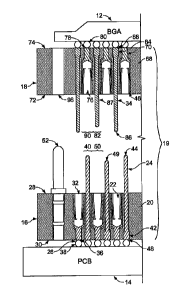
Referring to FIGS. 1, 2A, and 2B, a hermaphroditic socket/adapter assembly
10 for electrically connecting an IC package 12 to a PCB 14 is shown.
Hermaphroditic socket/adapter assembly 10, includes a first hermaphroditic
terminal
assembly 16 and a second hermaphroditic terminal assembly 18 that together
comprise an intercoupling component 19.
First hermaphroditic terminal assembly 16 includes an insulating support
member 20 for supporting female sockets 22 and male pins 24. Insulating
support
3
CA 02579155 2007-03-06
WO 2006/028633 PCT/US2005/028139
member 20 includes a first array of apertures 26, extending from the upper
surface 28
of insulating support member 20 to the bottom surface 30 of insulating support
member 20. Each female socket 22 is received within one aperture 26 of the
first
array of apertures of the insulating support member 20. Each female socket 22
has a
first end 32 configured to receive a corresponding male pin 34 of the second
hermaphroditic terminal assembly 18 and a second end 36 attached to a solder
ball 38
that establishes an electrical connection with the electrical contact 39 on
PCB 14. The
female sockets 22 received within the first array of apertures 26 of the
insulating
support member 20 are arranged such that interstitial spaces 40 exist between
the
female sockets 22.
Insulating support member 20 also includes a second array of apertures 42,
extending from the upper surface 28 of insulating support member 20 to the
bottom
surface 30 of insulating support member 20. Each male pin 24 is received
within one
aperture 42 of the second array of apertures of the insulating support member
20.
Each male pin has a first end 44 configured to be received within a
corresponding
female socket 46 of the second hermaphroditic terminal assembly 18 and a
second
end 48 attached to a solder ball 38 that establishes an electrical connection
with
electrical contact 39 on PCB 14. In some applications, it may be desirable for
at least
one male pin 49 to be of a different height than every other male pin 24 where
the
height of a pin is defined as the length from the first end of the pin 44 to
the second
end of the pin 48. Varying the height of the pins serves to decrease the force
required
to insert the first hermaphroditic terminal assembly 16 into a corresponding
hermaphroditic terminal assembly. Varying the height of the pins also serves
to
decrease the force required to extract the first hermaphroditic terminal
assembly 16
from a corresponding hermaphroditic terminal assembly into which it has been
inserted. The male pins 24 received within the second array of apertures 42 of
the
insulating support member 20 are arranged such that interstitial spaces 50
exist
between the male pins 24. Collectively, the female sockets 22 and the male
pins 24
are arranged in a pattern such that the interstitial spaces 40 between the
female
sockets 22 are occupied by male pins 24, and the interstitial spaces 50
between the
male pins 24 are occupied by female sockets 22. It is appreciated that the
female
sockets 22 and the male pins 24 could be arranged in different patterns.
4
CA 02579155 2007-03-06
WO 2006/028633 PCT/US2005/028139
First hermaphroditic terminal assembly 16 also includes two alignment guide
posts 52 located in opposite corners 54, 56 of first hermaphroditic terminal
assembly
16 and disposed through the upper surface 28 of the insulating support member
20
and two alignment guide holes 58 located in opposite corners 60, 62 of the
upper
surface 28 of the insulating support member 20. In addition, first
hermaphroditic
terminal assembly 16 includes two alignment guide posts 64 located in opposite
corners 54, 56 of first hermaphroditic terminal assembly 16 and disposed
through the
lower surface 30 of the insulating support member 20 and two alignment guide
holes
(not shown) located in opposite corners 60, 62 of the lower surface 30 of the
lo insulating support member 20.
Second hermaphroditic terminal assembly 18 includes an insulating support
member 68 for supporting female sockets 46 and male pins 34. Insulating
support
member 68 includes a first array of apertures 70, extending from the upper
surface 72
of insulating support member 68 to the bottom surface 74 of insulating support
member 68. Each female socket 46 is received within one aperture 70 of the
first
array of apertures of the insulating support member 68. Each female socket 46
has a
first end 76 configured to receive a corresponding male pin 24 of the first
hermaphroditic terminal assembly 16 and a second end 78 configured to contact
a
solder ball 80 on IC package 12. The female sockets 46 received within the
first array
of apertures 70 of the insulating support member 68 are arranged such that
interstitial
spaces 82 exist between the female sockets 46.
Insulating support member 68 also includes a second array of apertures 84,
extending from the upper surface 72 of insulating support member 68 to the
bottom
surface 74 of insulating support member 68. Each male pin 34 is received
within one
aperture 84 of the second array of apertures of the insulating support member
68.
Each male pin has a first end 86 configured to be received within a
corresponding
female socket 22 of the first hermaphroditic terminal assembly 16 and a second
end
88 configured to contact a corresponding solder ball 80 on IC package 12. In
some
applications, it may be desirable for at least one male pin 87 to be of a
different height
than every other male pin 34, where the height of a pin is defined as the
length from
the first end of the pin 86 to the second end of the pin 88. Varying the
height of the
pins serves to decrease the force required to insert the second hermaphroditic
terminal
assembly 18 into a corresponding hermaphroditic terminal assembly. Varying the
5
CA 02579155 2007-03-06
WO 2006/028633 PCT/US2005/028139
height of the pins also serves to decrease the force required to extract the
second
hermaphroditic terminal assembly 18 from a corresponding hermaphroditic
terminal
assembly into which it has been inserted. The male pins 34 received within the
second array of apertures 84 of the insulating support member 68 are arranged
such
that interstitial spaces 90 exist between the male pins 34. Collectively, the
female
sockets 46 and the male pins 34 are arranged in a pattern such that the
interstitial
spaces 82 between the female sockets 46 are occupied by male pins 34, and the
interstitial spaces 90 between the male pins 34 are occupied by female sockets
46. It
is appreciated that the female sockets 46 and the male pins 34 could be
arranged in
lo different patterns.
Second hermaphroditic terminal assembly 18 also includes two alignment
guide posts 92 located in opposite corners 94, 96 of second hermaphroditic
terminal
assembly 18 and disposed through the upper surface 72 of the insulating
support
member 68 and two alignment guide holes 98 located in opposite corners 100,
102 of
the upper surface 72 of the insulating support member 68. In addition, second
hermaphroditic terminal assembly 18 includes two alignment guide posts 104
located
in opposite corners 94, 96 of second hermaphroditic terminal assembly 18 and
disposed through the lower surface 74 of the insulating support member 68 and
two
alignment guide holes 98 located in opposite corners 100, 102 of the lower
surface 74
of the insulating support member 68.
The intercoupling component 19 is used to electrically connect IC package 12
to PCB 14. IC package 12 is secured to the lower surface 74 of insulating
support
member 68 of the second hermaphroditic terminal assembly 18 such that the
solder
balls 80 on IC package 12 are brought into contact with the second ends 78 of
the
female sockets 46 of the second hermaphroditic terminal assembly 18 and the
second
ends 88 of the male pins 34 of the second hermaphroditic terminal assembly 18.
The
alignment guide posts 104 disposed through the lower surface 74 the insulating
support member 68 of the second terminal assembly can be used to properly
align the
solder balls 80 on IC package 12 with the second ends 78 of the female sockets
46 of
the second hermaphroditic terminal assembly 18 and the second ends 88 of the
male
pins 34 of the second hermaphroditic terminal assembly 18. It is appreciated
that
other alignment elements could be used to facilitate proper alignment of the
solder
balls 80 on IC package 12 with the second ends 78 of the female sockets 46 of
the
6
CA 02579155 2007-03-06
WO 2006/028633 PCT/US2005/028139
second hermaphroditic terminal assembly 18 and the second ends of the male
pins 34
of the second hermaphroditic terminal assembly 18. It is also appreciated that
alignment elements are not required to properly align the electrical contacts
80 on IC
package 12 with the second ends 78 of the female sockets 46 of the second
hermaphroditic terminal assembly 18 and the second ends of the male pins 34 of
the
second hermaphroditic terminal assembly 18.
Hermaphroditic socket/adapter assembly 10 includes a hold-down cover 108
for securing the IC package 12 to the intercoupling component 19. Hold-down
cover
108 includes a pair of opposite walls 110 having tab members 112 that engage
the
lo intercoupling component 19. Hold-down cover 108 includes a threaded thru-
hole 114
that threadingly receives a heat sink 116 to provide a thermal path for
dissipating heat
from the IC package 12. Heat sink 116 is inserted through threaded thru-hole
114 and
a slot 118 formed in the heat sink 116 facilitates threading the heat sink 116
within the
cover, for example, with a screwdriver or coin. It is appreciated that other
mechanisms may also be used to secure the IC package 12 to the intercoupling
component 19. It is also appreciated that other heat sink arrangements may be
substituted for the version shown in FIG. 1. In some applications, a heat sink
may not
be required. Therefore, it is appreciated that the hold-down cover 108 may be
used to
secure the IC package 12 to the intercoupling component 19 without a heat
sink. It is
also appreciated that the hold-down cover itself may not be necessary to
secure the IC
package 12 to the intercoupling component 19. In some applications, the IC
package
12 may be soldered directly to the intercoupling component 19.
The second hermaphroditic terminal assembly 18 is coupled to the first
hermaphroditic terminal assembly 16 by inserting each male pin 34 of the
second
terminal assembly 18 into a corresponding female socket 22 of the first
hermaphroditic terminal assembly 16 and inserting each male pin 24 of the
first
hermaphroditic terminal assembly 16 into a corresponding female socket 46 of
the
second hermaphroditic terminal assembly 18. When the second hermaphroditic
terminal assembly 18 is coupled to the first hermaphroditic terminal assembly
16, it is
said to be mated with the first hermaphroditic terminal assembly 16. The
alignment
guide posts 92 disposed through the upper surface 72 of the insulating support
member 68 of the second hermaphroditic terminal assembly 18 are inserted into
alignment guide holes 58 in the upper surface 28 of the insulating support
member 20
7
CA 02579155 2007-03-06
WO 2006/028633 PCT/US2005/028139
of the first hermaphroditic terminal assembly 16 and the alignment guide posts
52
disposed through the upper surface 28 of the first hermaphroditic terminal
assembly
16 are inserted into alignment guide holes 98 in the upper surface 72 of the
insulating
support member 68 of the second hermaphroditic terminal assembly 18 to
properly
align the male pins 34 of the second hermaphroditic terminal assembly 18 with
the
corresponding female sockets 22 of the first hermaphroditic terminal assembly
16 and
the male pins 24 of the first hermaphroditic terminal assembly 16 with the
corresponding female sockets 46 of the second hermaphroditic terminal assembly
18.
It is appreciated that other alignment elements could be used to facilitate
proper
lo alignment of the male pins 34 of the second hermaphroditic terminal
assembly 18
with the corresponding female sockets 22 of the first hermaphroditic terminal
assembly 16 and the male pins 24 of the first hermaphroditic terminal assembly
16
with the corresponding female sockets 46 of the second hermaphroditic terminal
assembly 18. It is also appreciated that alignment elements are not required
to
properly align the male pins 34 of the second hermaphroditic terminal assembly
18
with the corresponding female sockets 22 of the first hermaphroditic terminal
assembly 16 and the male pins 24 of the first hermaphroditic terminal assembly
16
with the corresponding female sockets 46 of the second hermaphroditic terminal
assembly 18. In some applications, it may be advantageous for the alignment
guide
posts 92 disposed through the upper surface 72 of insulating support member 68
of
the second hermaphroditic terminal assembly 18 and the alignment guide posts
52
disposed through the upper surface 28 of the first hermaphroditic terminal
assembly
16 to serve as power, voltage, or ground connections.
Referring to FIG. 1, first hermaphroditic terminal assembly 16 is identical to
second hermaphroditic terminal assembly 18. In order to connect first
hermaphroditic
terminal assembly 16 to second hermaphroditic terminal assembly 18, second
hermaphroditic terminal assembly 18 is rotated 90 degrees so that the male
pins 34 of
the second hermaphroditic terminal assembly 18 are aligned with corresponding
female sockets 22 of the first hermaphroditic terminal assembly 16 and the
male pins
24 of the first hermaphroditic terminal assembly 16 are aligned with
corresponding
female sockets 46 of the second hermaphroditic terminal assembly 18. It is
appreciated that the first hermaphroditic terminal assembly 16 need not be
identical to
the second hermaphroditic terminal assembly 18.
8
CA 02579155 2007-03-06
WO 2006/028633 PCT/US2005/028139
First hermaphroditic terminal assembly 16 is secured to PCB 14 such that the
solder balls 38 attached to second ends 36 of the female sockets 22 of the
first
hermaphroditic terminal assembly 16 and the solder balls 38 attached to second
ends
48 of the male pins 24 of the first hermaphroditic terminal assembly 16 are in
contact
with the electrical contacts 39 on PCB 14. The alignment guide posts 64
disposed
through the lower surface 30 of the insulating support member 20 of the first
hermaphroditic terminal assembly 16 are inserted into alignment guide holes
128 in
PCB 14. It is appreciated that other alignment elements could be used to
facilitate
proper alignment of the solder balls 38 attached to second ends 36 of the
female
lo sockets 22 of the first hermaphroditic terminal assembly 16 and the solder
balls 38
attached to second ends 48 of the male pins 24 of the first hermaphroditic
terminal
assembly 16 with the electrical contacts 39 on PCB 14. It is also appreciated
that
alignment elements are not required.
When IC package 12 is secured to the lower surface 74 of insulating support
member 68 of the second hermaphroditic terminal assembly 18 such that the
solder
balls 80 on IC package 12 are in contact with the second ends 78 of the female
sockets 46 of the second hermaphroditic terminal assembly 18 and the second
ends 88
of the male pins 34 of the second hermaphroditic terminal assembly 18; second
hermaphroditic terminal assembly 18 is coupled to the first hermaphroditic
terminal
assembly 16 such that each male pin 34 of the second hermaphroditic terminal
assembly 18 is received within a corresponding female socket 22 of the first
hermaphroditic terminal assembly 16 and each male pin 24 of the first
hermaphroditic
terminal assembly 16 is received within a corresponding female socket 46 of
the
second hermaphroditic terminal assembly 18; and first hermaphroditic terminal
assembly 16 is secured to PCB 14 such that that the solder balls 38 attached
to second
ends 36 of the female sockets 22 of the first hermaphroditic terminal assembly
16 and
the solder balls 38 attached to second ends 48 of the male pins 24 of the
first terminal
assembly 16 are in contact with the electrical contacts 39 on PCB 14, the IC
package
12 being electrically connected to PCB 14.
FIGS. 2A and 2B illustrate the operation of intercoupling component 19. The
solder balls 38 attached to second ends 36 of the female sockets 22 of the
first
hermaphroditic terminal assembly 16 and the solder balls 38 attached to second
ends
48 of the male pins 24 of the first hermaphroditic terminal assembly 16 are in
contact
9
CA 02579155 2007-03-06
WO 2006/028633 PCT/US2005/028139
with the electrical contacts 39 on PCB 14. Similarly, the second ends 78 of
the
female sockets 46 of the second hermaphroditic terminal assembly 18 and the
second
ends 88 of the male pins 34 of the second hermaphroditic terminal assembly 18
are in
contact with the solder balls 80 on IC package 12. Referring to FIG. 2A, IC
package
12 and PCB 14 are not electrically connected. Referring to FIG. 2B,
intercoupling
component 19 is used to electrically connect IC package 12 and PCB 14. The
electrical connection between IC package 12 and PCB 14 is formed by inserting
each
male pin 34 of the second hermaphroditic terminal assembly 18 into a
corresponding
female socket 22 of the first hermaphroditic terminal assembly 16 and
inserting each
lo male pin 24 of the first hermaphroditic terminal assembly 16 into a
corresponding
female socket 46 of the second hermaphroditic terminal assembly 18.
A number of embodiments of the invention have been described.
Nevertheless, it will be understood that various modifications may be made
without
departing from the spirit and scope of the invention. For example,
hermaphroditic
terminal assemblies can be used to electrically connect many different types
of
electrical devices. Referring to FIG. 3, intercoupling component 19, including
first
hermaphroditic terminal assembly 16 and second hermaphroditic terminal
assembly
18, are used to electrically connect a first PCB 120 to a second PCB 122. The
second
ends 36 of the female sockets 22 of the first hermaphroditic terminal assembly
16 and
the second ends 48 of the male pins 24 of the first hermaphroditic terminal
assembly
16 are connected to solder balls 124 and form an electrical connection with
the
electrical contacts 125 on first PCB 120. Similarly, the second ends 78 of the
female
sockets 46 of the second hermaphroditic terminal assembly 18 and the second
ends 88
of the male pins 34 of the second hermaphroditic terminal assembly 18 are
connected
to solder balls 126 and form an electrical connection with the electrical
contacts 127
on second PCB 122. The electrical connection between first PCB 120 and second
PCB 122 is formed by inserting each male pin 34 of the second hermaphroditic
terminal assembly 18 into a corresponding female socket 22 of the first
hermaphroditic terminal assembly 16 and inserting each male pin 24 of the
first
hermaphroditic terminal assembly 16 into a corresponding female socket 46 of
the
second hermaphroditic terminal assembly 18. Accordingly, other embodiments are
within the scope of the following claims.