Note: Descriptions are shown in the official language in which they were submitted.
CA 02579217 2013-07-04
1
ULTRATHIN LIGHTING ELEMENT
Field of the Invention
The present invention relates to lightguides for guiding light from light
sources in
lighting solutions. The lightguides may include ultra thin lightguide layers
and multi-layer
applications. Additionally, the present invention includes lighting elements
that include the
lightguides and lighting solutions. The present invention also relates to
manufacturing methods.
The lightguides and lighting elements can be used for display lighting (e.g.
backlighting,
frontlighting), interior lighting and exterior lighting, among other
applications.
Summary of the Invention
In accordance with an aspect of the present invention, there is provided an
ultra thin
lighting element, comprising: at least one light source; and a flexible
lightguide element
comprising one lightguide layer comprising a plurality of discrete groups of
fine optic surface
relief structures disposed on at least one portion of at least one surface of
the light guide element,
each discrete group comprising basic structural features on the order of about
10 microns or less
in height, and less than 10 microns in one lateral dimension, wherein the
surface relief structures
are arranged in a regular pattern within each discrete group, wherein the at
least one light source
is arranged at at least one edge of the lightguide element, wherein the
lightguide element laterally
incouples light from the at least one lightsource into the lightguide element
transmits the light
through the lightguide element and outcouples light from a surface of the
lightguide element,
wherein at least a portion of the light is outcoupled from the surface of the
lightguide element in
a direction perpendicular to the surface of the lightguide element in the
vicinity of the
outcoupling. The number, arrangement and size of each surface relief structure
and height and
lateral dimensions of the structural features of the surface relief structures
are varied to provide a
desired degree of outcoupling modulation of light incoupled into the
lightguide element.
In accordance with another aspect of the present invention, there is provided
an ultra thin lighting
element, comprising: at least one light source; and a foldable lightguide
element comprising one
CA 02579217 2013-07-04
2
lightguide layer comprising a plurality of discrete groups of fine optic
surface relief structures
disposed on at least one portion of at least one surface of the foldable
lightguide element, each
discrete group comprising basic structural features on the order of about 10
microns or less in
height, and less than 10 microns in one lateral dimension, wherein the surface
relief structures
are arranged in a regular pattern within each discrete group, wherein the at
least one light source
is arranged at at least one edge of the lightguide element, wherein the
lightguide element laterally
incouples light from the at least one lightsource into the lightguide element
transmits the light
through the lightguide element and outcouples light from a surface of the
lightguide element,
wherein at least a portion of the light is outcoupled from the surface of the
lightguide element in
a direction perpendicular to the surface of the lightguide element in the
vicinity of the
outcoupling. The number, arrangement and size of each surface relief structure
and height and
lateral dimensions of the structural features of the surface relief structures
are varied to provide a
desired degree of outcoupling modulation of light incoupled into the
lightguide element.
In accordance with another aspect of the present invention, there is provided
an ultra thin lighting
element, comprising: at least one light source; and a lightguide element
comprising at least one
lightguide layer comprising a plurality of discrete groups of fine optic
surface relief structures on
at least one portion of at least one surface, each discrete group comprising
basic structural
features on the order of 10 microns or less in height, and less than 10
microns in at least one
lateral dimension, wherein the number, arrangement and size of each surface
relief structure and
height and lateral dimensions of the structural features of the surface relief
structures are varied
to provide a desired degree of outcoupling modulation of light incoupled into
the lightguide
element; and the surface relief structures are arranged in small discrete
outcoupling structure
groups having a distance therebetween of up to about 300 microns in a region
of the at least one
lightguide layer in the vicinity of the at least one point light source.
In accordance with another aspect of the present invention there is provided a
lighting
element, comprising: at least one light source; and a lightguide element
comprising at least one
lightguide layer comprising a plurality of discrete groups of fine optic
surface relief structures
disposed on at least one portion of at least one surface, of the lightguide
element each discrete
group comprising structural features on the order of 10 microns or less in
height, and less than 10
CA 02579217 2013-07-04
2a
microns in at least one lateral dimension, wherein: the number, arrangement
and size of each
surface relief structure and height and lateral dimensions of the structural
features of the surface
relief structures are varied to provide a desired degree of outcoupling
modulation of light
incoupled into the lightguide element; and the surface relief structures are
arranged in small
discrete outcoupling structure groups having a distance therebetween of up to
about 300 microns
in a region of the at least one lightguide layer in the vicinity of the at
least one light source.
In accordance with another aspect of the present invention, there is provided
a lighting
element, comprising: at least one light source; and a lightguide element
comprising at least one
lightguide layer comprising a plurality of discrete groups of fine optic
surface relief structures
disposed on at least one portion of at least one surface, of the lightguide
element each discrete
group comprising structural features on the order of 10 microns or less in
height, and less than 10
microns in at least one lateral dimension, wherein: the number, arrangement
and size of each
surface relief structure and height and lateral dimensions of the structural
features of the surface
relief structures are varied to provide a desired degree of outcoupling
modulation of light
incoupled into the lightguide element; the surface relief structures are
arranged in a region of the
at least one lightguide layer in the vicinity of the at least one light source
in small discrete
outcoupling structure groups comprising some of the area, up to about 10% of
the area of the at
least one lightguide layer in the region; and the surface relief structures
are arranged in small
discrete outcoupling structure groups having a distance therebetween of up to
about 300 microns
in the region of the at least one lightguide layer in the vicinity of the at
least one light source.
Further objectives and advantages, as well as the structure and function of
exemplary
embodiments will become apparent from a consideration of the description,
drawings, and
examples.
Brief Description of the Drawings
The foregoing and other features and advantages of the invention will be
apparent from
the following, more particular description of an exemplary embodiment of the
invention, as
illustrated in the accompanying drawings wherein like reference numbers
generally indicate
identical, functionally similar, and/or structurally similar elements.
CA 02579217 2013-07-04
2b
Figs, la and lb represent illustrations showing cross-sectional views of two
embodiments
of known lightguide structures;
Figs. 2a, 2b, and 2c represent illustrations showing cross-sectional views of
various
embodiments of ultrathin lighting elements according to the present invention;
Fig. 3 represents an illustration showing a perspective view of an embodiment
of an
ultrathin lighting element according to the present invention;
CA 02579217 2006-10-27
WO 2005/107363
PCT/1B2005/002334
3
Figs. 4a and 4b represent illustrations showing cross-sectional views of
embodiments of
an ultrathin lighting elements according to the present invention including
curved lightguide
elements;
Fig. 5a represents an illustration showing a cross-sectional view of an
embodiment of a
lighting element according to the present invention that includes a matrix
including a plurality of
lighting elements;
Fig. 5b represents an illustration showing a cross-sectional view of an
embodiment of a
lighting elements according to the present invention including a bendable
lightguide element;
Figs. 6a, 6b, 6c, and 6d represent illustrations showing cross-sectional views
of
embodiments of lighting elements according to the present invention that
include lightguide
elements including two lightguide layers;
Figs. 7a, 7b, and 7c represent illustrations showing cross-sectional views of
embodiments
of lighting elements according to the present invention that include
lightguide elements including
two lightguide layers and including various optical relief structures
optionally on various
surfaces on various surfaces and optionally various films arranged between the
layers;
Figs. 8a, 8b, and 8c represent illustrations showing cross-sectional views of
embodiments
of lighting elements according to the present invention that include
lightguide elements including
CA 02579217 2006-10-27
WO 2005/107363
PCT/1B2005/002334
4
two or more lightguide layers, optionally in various regions, and including
various optical relief
structures optionally on.various surfaces on various surfaces and optionally
various films
arranged between the layers;
Fig. 9a represents an illustration showing a cross-sectional view of an
embodiment of a
lighting element according to the present invention wherein a portion of the
lightguide element
includes two lightguide layers and a bendable lightguide layer;
Figs. 9b and 9c represent illustrations showing cross-sectional views of
embodiments of a
lighting elements according to the present invention that include a single
lightguide layer bent to
form a two layer lightguide element;
Figs. 10a and 10b represent illustrations showing overhead views of
embodiments of a
lighting element according to the present invention;
Fig. 11 represents an illustration showing an overhead view of a lighting
element
according to the present invention illustrating various sizes that the
embodiment of the lightguide
element;
Figs. 12a, 12b, and 13 represent illustrations showing overhead views of
embodiments of
lightguide elements according to the present invention that include various
patterns of surface
relief structures over the lightguide elements;
CA 02579217 2006-10-27
WO 2005/107363
PCT/1B2005/002334
Figs. 14 and 15 represent illustrations showing cross-sectional views of
embodiments for
manufacturing lightguide layers according to the present invention utilizing
roll-to-roll
production;
5 Fig. 16 represents and illustration showing a cross-sectional view of
embodiments for
manufacturing lightguide layers according to the present invention utilizing
ultraviolet (UV)
casting;
Figs. 17a, 17b and 17c represent illustrations showing overhead views of
embodiments of
lightguide layers according to the present invention;
Fig. 18 represents an illustration showing a cross-sectional view of an
embodiment of a
keypad including a lighting element according to the present invention;
Figs. 19a, 19b, and 19c represent illustrations showing various embodiments of
lightguide layers according to the present invention including surface relief
structures arranged in
various groupings;
Figs. 20a and 20b represent illustrations showing, respectively, an overhead
view and a
side view of an embodiment of a lighting element according to the present
invention where the
incoupling structure includes optic fibers;
Figs. 21a and 21b represent illustrations showing overhead views of lightguide
elements
CA 02579217 2012-10-26
6
according to the present invention including surface relief structures in
different
groupings in a region of the lightguide layer in the vicinity of the light
sources;
Figs. 22a and 22b represent illustrations showing an overhead view and a cross-
sectional view of an embodiment of a lightguide layer wherein the basic
structural
features of the surface relief structures form a small discrete outcoupling
structure
groups;
Figs. 23 a and 23b represent illustrations showing an overhead view and a
cross-
sectional view of an embodiment of a lightguide layer wherein the different
basic
structural features of surface relief structures are forming small discrete
outcoupling
structure groups; and
Figs. 24a and 24b represent illustrations showing cross-sectional views of
various
embodiments of basic structural features of surface relief structures
according to the
present invention.
Detailed Description of Embodiments of the Invention
Embodiments of the invention are discussed in detail below. In describing
embodiments, specific terminology is employed for the sake of clarity.
However, the
invention is not intended to be limited to the specific terminology so
selected. While
specific exemplary embodiments are discussed, it should be understood that
this is done
for illustration purposes only. A person skilled in the relevant art will
recognize that other
components and configurations can be used.
CA 02579217 2006-10-27
WO 2005/107363
PCT/1B2005/002334
7
The present invention provided a lighting element that includes a lightguide
element.
The lightguide element includes at least one lightguide layer. The lightguide
layer(s) may be
made of a variety of different materials. Typically, any optically clear
material may be utilized.
Examples of materials that may be utilized include PMMA, PC, PET and other
polymers. The
materials may be clear UV or thermal cured.
Circuitry, electrical contacts, printed figures or masks may be applied on one
or more
lightguide layers.
The at least one lightguide layer includes a plurality of discrete fine optic
surface relief
structure groups on at least one portion of at least one surface. The surface
relief structure group
may be provided on at least a portion of each side of each lightguide layer.
Each surface relief
structure group is made up of basic structural features. The structural
features can include
(discrete or non-continuous) grooves having various cross-sections, such as
different cross-
sectional wave forms. The surface relief structures may include diffractive
and/or refractive
structures. The structural features can have any cross-sectional shape such
that they can
outcouple light from the lightguide layer. The outcoupling from group to group
may be the
same, such as with a keypad. On the other hand, the outcoupling of each group
may be different.
It may even be desirable to vary the outcoupling of one group at different
locations in the group.
The structural features can have any cross-sectional shape such that they can
outcouple
light from the lightguide layer. For example, the optic surface relief
structure for light
CA 02579217 2006-10-27
WO 2005/107363
PCT/1B2005/002334
8
outcoupling is typically a fine grating structure. The grating profile can be
binary, blazed,
slanted and sinusoidal or hybrid, among other shapes. The light outcoupling
structure of
lightguide layer can be designed in order to form uniform illumination on the
whole surface or
discrete illumination in the preferred areas with preferred shape. The grating
structures can be
optimised in order to achieve high outcoupling efficiency in 00 angle
(collimated light) utilizing,
for example, blazed type grating.
The surface relief structures may be arranged over the entire surface or
substantially the
entire surface of a lightguide layer. Alternatively, the surface relief
structures may be confined
to all of one region of a lightguide layer. In some embodiments, the surface
relief structures are
confined to certain regions of the at least one lightguide layer. The regions
may be regularly or
irregularly arranged on any lightguide layer. The desired degree of
outcoupling may affect the
arrangement of the surface relief structures. The proximity to the light
source(s) may also affect
the arrangement of the surface relief structures. For example, a region of the
lightguide layer in
the vicinity of the at least one light source the outcoupling structure groups
comprise aboUt 10%
or less of the area of the lightguide layer.
Each surface relief structure includes basic structural features. The
dimensions of the
basic features may depend upon the desired degree of outcoupling and the
wavelengths of light
being utilized. Typically, the basic features are on the order of about 10
microns or less in
height, and on the order of about 10 microns or less in each lateral
dimension. More typically,
the basic features are on the order of less than about 10 microns in height,
and on the order of
less than about 10 microns in each lateral dimension.
CA 02579217 2012-10-26
9
Figs. 24a and 24b represent illustrations showing cross-sectional views of
various
embodiments of basic structural features of surface relief structures
according to the
present invention. These shapes represent only a few examples of the cross-
sectional
shapes that the basic structural elements may have. Any lightguide layer may
include
anyone or more of these shapes in any region of surface relief structures. To
facilitate the
understanding of these features, the features are illustrated in a few
discrete groups. As is
apparent from the discussion herein, the surface relief structures may be
provided
anywhere on any lightguide layer.
The lightguide element may include more than one lightguide layer. If the
lighting
element includes more than one lightguide layer, the lightguide layers may
have the same
cross-sectional area. Alternatively, the lightguide layers may have different
cross-
sectional areas. The number of lightguide layers may vary over the lightguide
element.
The thickness of the single lightguide layer may be about 0.01mm to about 0.4
mm. The
lightguide element may have a thickness similar to the height of the light
source.
The entire lightguide element may be planar. At least a portion of one or more
of the
lightguide element may be flexible and/or bendable. The bend may be permanent
or the
lightguide element may be bent during use. The lightguide is flexible in the
sense that
light can still be propagated through it and outcoupled out of it on either
side of curve or
bend. If the lightguide element includes more than one lightguide layer, one
or more the
lightguide layers may be bendable and/or flexible. When at least a portion of
the
lightguide element is curved, the angle of the curve typically does not exceed
a total
reflection angle.
CA 02579217 2006-10-27
WO 2005/107363
PCT/1B2005/002334
If the lightguide element includes more than one lightguide layer, one or more
films may
be arranged at least a portion of any region between overlying two lightguide
layers. A variety
of different films may be arranged between lightguide layers. For example, the
film can include
5 one or more of reflector film, diffuser film, prismatic film and
brightness enhancement film, in
order to form different lighting performances.
At least one light source produces light that is introduced into the
lightguide element.
The light source could include an LED or other suitable light source. The
light is incoupled into
10 the lightguide element. The light source could be connected directly to
the lightguide element
and directly introduce light into the lightguide element. Alternatively, the
lighting element may
be arranged with one or more incoupling structures. The incoupling structure
may include a
wedge including specular reflectors on at least one of a top and bottom
surface, an elliptical light
pipe, a focusing lens and/or a bundle of split optic fibers. The light source
and the incoupling
structure may be a unitary structure. Where the lightguide element includes
multiple lightguide
layers, the incoupling may vary among the layers. Some embodiments of the
incoupling
structure may include a slanted, a blazed or a radial binary grating structure
with or without
diverging lens.
The present invention provides great advantages over known lightguide
structures,
particularly in terms of providing a thin and flexible structure. For example,
an ultra thin
lightguide, which requires less space. This can be a very important issue
especially in hand held
products such as mobile phones, watches, but also in other display, keypad,
console and lighting
CA 02579217 2006-10-27
WO 2005/107363
PCT/1B2005/002334
11
solutions.
Embodiments of a thin, flexible lightguide according to the invention that can
be bent can
allow making interesting applications, such as flexible and/or curved
displays, flexible phones,
clam shell mobile phones (flip-phones). Embodiments of the present invention
that include
multiple lightguide layers offer the ability to easily control light
incoupling/outcoupling and
other optical performances, in each layer. Two or more lightguide layers can
be stacked on top
of another. Reflector and/or films can be utilized between these.
Light may be incoupled into the lightguide layers in proportion to layer
thickness. Along
these lines, thickness typically incouples less light, whereas more thickness
typically incouples
more light. This can provide a very easy way to control the light incoupling
and can also
distribute the light to different lightguide layers. This concept is suitable
for dual backlights,
backlights with keypad lighting, dual backlights with keypad lighting, among
other structures.
The total thickness of the lightguide stack-up can be the same as the height
of the LED.
For example, according to one embodiment, the LED has a height of about 0.8
mm.
The present invention may include a centralized light source arrangement. This
typically
requires less light sources (e.g. LEDs), less assembly costs and less space.
Embodiments of the
present invention that include multi-layer lightguide layers can utilize light
sources that are
placed on only one edge of the lightguide stack up. All lightguide layers may
propagate light to
the right area, in order to be illuminated.
CA 02579217 2006-10-27
WO 2005/107363
PCT/1B2005/002334
12
Embodiments of the present invention can provide practical variability in the
size of the
lightguide and the amount of light sources. This can provide more flexibility
to utilize the same
lightguide design in different applications. The lightguide design may be
formed for a specific
size with a specific optical diffusing structure or light directing structure
in the first (light
incoupling) part, which is in the vicinity of the light source(s), which is
not dependent on precise
light source (e.g. LED) placement. This type of optical design can allow the
use of different
amounts of light sources, while having the minimum quantity of light sources
and maximum
quantity of light sources on the same edge. This can permit achieving higher
or lower brightness
with the same uniformity performance. Additionally, the same lightguide design
can be cut to
different sizes in order to achieve the same performance in uniformity.
The present invention can provide extremely cost-effective production. For
example, the
surface relief structure may be formed by means of a continuous roll
replication process (roll-to-
roll process). This method offers extremely fast production, with high optical
product quality.
Conventional thin lightguides typically have a thickness of about 0.8 to about
1,0 mm and
typically include microlens or microstructures. Such conventional
microstructures, such on the
order of about 15 microns in height or more, and on the order of about 50
microns or more in one
lateral dimension, cannot be utilized in thin flexible lightguides for a
variety of reasons. For
example, these optical structures are unable to function properly with large
incidence angles.
Additionally, these optical structures have a limited degree of modulation, to
achieve uniform
light outcoupling distribution in thin lightguide solution. Furthermore,
conventional production
CA 02579217 2006-10-27
WO 2005/107363
PCT/1B2005/002334
13
methods, such as injection molding, can cause problems with optical quality in
thin lightguide
solutions.
Preferred embodiments of the present invention can provide an ultra thin
lightguide (film-
like) solution with a single layer thickness of about 0.4¨ about 0.01 mm.
Embodiments of the
present invention can include lightguides with single layer and multilayer
solutions. All layers
may have surface relief structures, which may be formed on the surface in
order to achieve
different optical functions. These optical structures can be diffractive
and/or refractive having
different profiles such as binary, slanted, blazed, and sinusoidal, etc.,
forming different light
outcoupling groups or sub-groups.
Multilayer lightguide elements according to the present invention may have a
thickness
that may be matched by the height of the light source. For example, if the
light source includes
an LED, the LED may have a height of about 0.8 mm, the lightguide element may
include
multiple lightguide layers and a reflector arranged between the layers may
have a height of about
0.8 mm. The light incoupling and luminance (brightness) may be controlled by
varying the
thickness of each lightguide layer. For example, light from the light source
may incoupled into
the lightguide layers in proportion to layer thickness. Along these lines,
less thickness = less
light incoupling and less brightness, more thickness = more light incoupling
and more
brightness. This is a very simple way to control the light incoupling and
distributes the light to
the different lightguide layers, permitting a controlled and desired
brightness to be realized in
each of the lightguide layers.
CA 02579217 2006-10-27
WO 2005/107363
PCT/1B2005/002334
14
The lightguide layers according to the present invention may be manufactured
according
to a number of different processes. Thin lightguide layer production is
preferably completed by
means of continuous roll replication, or roll-to-roll replication. Using this
fast, cost-effective
manufacturing method bulk material, such as optically clear plastic film, can
be utilized in
surface relief replication. These different well know roll-to-roll methods are
well known and
well sophisticated to manufacture surface relief structures, either refractive
or diffractive for
many different applications. There are several published material and many
companies having
patented roll-to-roll methods available, such as Reflexite, Avery Dennison,
3M, Epigem,
Rolltronics, Polymicro, Printo project, among others. Additionally, high
quality replicated
optical structures can be achieved.
Other suitable production methods can include continuous or discrete casting
methods
(UV or thermal curing), compression molding, continuous or discrete embossing,
such as hard
embossing, soft embossing and UV embossing, among others. Melt film can also
be used.
Although many manufacturing processes may be utilized, some may be
particularly suitable to
manufacturing particular embodiments. For example, blazed type structural
profiles may be best
manufactured by means of roll-to-roll UV-embossing or a melt film method, in
order to achieve
accurate and high quality replication.
Other functional films, such as reflector films, can be laminated onto the
surface of
lightguide during the same roll-to-roll production method. Also, any kind of
figures and mask
can be printed or laminated on the lightguide layer including electrical
contact and circuitries.
This can be a crucial cost issue.
CA 02579217 2006-10-27
WO 2005/107363
PCT/1B2005/002334
15 .
After the surface relief structures are formed, the lightguide layers can be
cut to preferred
shapes directly from a roll or film by means of laser, die cutting and/or
other means. Also,
optical features can be manufactured during the cutting process. Such optical
features
particularly include narrow boundary lines, which can be reflecting or
directing light for the
preferred area, or directing/diffusing light in the first part of lightguide.
This cutting process can
be completed in the roll-to-roll process with very short unit times and costs.
Injection molding as a production method may make it difficult to manufacture
ultra thin
lightguides in sizes larger than about 10"/15". The reason for this is that
fine optic structures,
such as surface relief structures on the order of about 15 microns and less,
may be difficult to
replicate totally/perfectly and at the same time achieve a high quality yield.
The optical structure, or surface relief structure, of a thin lightguide
typically requires a
high and increased degree of modulation to achieve the uniform light
outcoupling distribution, or
brightness. The optical basic structure typically must be very fine, such as
on the order of
smaller than about 10 microns or less in height, and on the order of about 10
microns or less in
one lateral dimension, in order to achieve the desired degree of modulation.
This makes it
possible to form small discrete outcoupling structure groups and control the
proportion of
outcoupling structures on the lightguide layer more accurately. Preferably, in
thin lightguide
layers, the optical structures are arranged in small discrete outcoupling
structure groups, wherein
a region of the lightguide layer in the vicinity of the at least one light
source the outcoupling
structure groups comprise about 10% or less of the area of the lightguide
layer. In this region the
CA 02579217 2006-10-27
WO 2005/107363
PCT/1B2005/002334
16
maximum distance between small discrete outcoupling structure groups is 300
microns or less.
This region may be the most crucial part of the lightguide structural design,
because an intensity
of incoupled light can be 50% or more of maximum intensity.
Conventional microstructure solutions that are based on bigger and higher
optical details,
typically have difficulties in thin lightguides in order to achieve uniform
brightness.
Embodiments of a lightguide element according to the present invention can be
flexible.
In some cases, less than all lightguide layers of a lightguide element may be
flexible.
Embodiments of the invention including a flexible lightguide element can be
bent into a desired
form. Such embodiments can be flexible and curved (bent) for preferred form in
order to fulfill
total reflection theory and not exceeding the total reflection angle.
A thin lightguide can help to prevent light leakage, because light beams
typically hit the
optical structure more times than in a thicker lightguide. The total light can
be outcoupled more
efficiently, causing less light leakage at the end of the lightguide.
Ultra thin lightguides can be used as a single layer with or without other
optic films
(reflector, diffusers, brightness enhancement films). Thin lightguide layer
can have fine optical
structures, either on one side or both sides of the layer.
In order to use only one lightguide layer, a conventional LED may be adapted
to the
lightguide layer with a specific optical component or adapter, which helps to
incouple light into a
CA 02579217 2006-10-27
WO 2005/107363
PCT/1B2005/002334
17
thin lightguide layer. For example, the LED height may be 0.8 mm as compared
to a lightguide
layer having a thickness of about 0.2 mm. This LED optical component or
adapter could be, for
example, a wedge-type solution with specular reflectors on the top and bottom.
Other incoupling
structures that may be utilized can include a thin elliptical light pipe, a
focusing lens or a bundle
of split optic fibers. Also, LEDs with circuitry can be in-molded into this
adapter. This can
make it easier to handle them. This adapter can contain snap structures in
order to connect it to
the lightguide layer easily. This adapter can be made of either rigid or
flexible optical material.
Process methods for forming the adapter can be, for example, casting or
injection molding.
Light incoupling may be completed with specific grating structures on the
bottom or on the top
surface. For example, a slanted, a blazed or radial binary grating structure
may be utilized with
or without a diverging lens.
Ultra thin lightguide elements can be constructed with two or more layers.
Lightguide
layers can form, for example, a dual backlight solution, backlight and keypad
lighting solution,
dual backlight and keypad lighting solution. For dual backlight solution, only
one reflector film
between lightguide layers may be required. This can cut costs and makes the
package thinner
and easier to handle and assemble. In a solution that includes two layers, the
optical outcoupling
structures can be arranged in the center line of the lightguide solution
(inner surfaces of
lightguide layers), because the major part of incoupled light may be
propagated along a center
line. In the words, the majority of light may be propagated at high incidence
angles.
One or more lightsources may be arranged to provide light that is introduced
into the
lightguide element. According to some embodiments, all light sources can be
placed on the one
CA 02579217 2006-10-27
WO 2005/107363
PCT/1B2005/002334
18
edge of a lightguide element for light incoupling into the lightguide layers.
This centralized light
source arrangement may reduce the amount of needed light sources and remove
the need for a
light source multi-assembly. This can have a direct influence on total cost
reductions.
One preferred application is the backlight and keypad combination, where a
centralized
LED arrangement can be used on the edge of lightguide stack up. The same LEDs
can provide
illumination for the backlight and keypad. In conventional solutions separate
LEDs for both the
backlight and keypad illumination must be used.
The optical structure of the lightguide layer can be designed with variation
capabilities
concerning its size and the amount of light sources that it incorporates. The
optical lightguide
design in the first part (light incoupling part) of the lightguide structure
can be optimized in such
a manner that the light from a point source, such as an LED, may be diffused
at different conical
angles or directed partially at the same angle, in order to achieve more
uniform and/or directed
light distribution in the first part. The optical design of the lightguide is
not dependent on an
exact light source placement. This type of optical design allows the use of
different numbers of
light sources, having a minimum quantity of light sources and a maximum
quantity of light
sources on the same edge in order to achieve higher and lower brightness with
same uniformity
performance. This type of optic surface relief structure may be placed on the
top and the bottom
surface of the first part of lightguide layer, having diffractive or
refractive grooves.
The outcoupling structure may be optimised a manner that it can allow cutting
and using
the same lightguide design in different sizes in order achieve the same
uniformity performance.
CA 02579217 2006-10-27
WO 2005/107363
PCT/1B2005/002334
19
This can make a lightguide solution more variable and flexible to utilize it
in different solutions
and applications, without the need to design many lightguide elements, which
may have only
slight differences in brightness and size requirements.
Conventional known keypad, keyboard and console lighting typically includes 3-
8 LEDs
and a thick lightguide having holes for each keys or buttons in order to make
electrical contact.
Such designs include electric circuitry with the help of dome sheet that
includes plurality of thin
metal domes, one per each key or button. When pushing the key or the button,
the thin metal
dome on the sheet is bent and flattened making electrical contact, for
example, on the surface of
electric circuitry. The dome also provides touch feeling with a click effect.
The holes are
needed to make such designs function. However, these holes make it difficult
to manage light in
order to achieve uniform keypad lighting.
On the other hand, an ultra thin lightguide layer according to the present
invention can be
used in keypad lighting, having a thickness of about 50 to about 200 microns,
which provides a
good flexible and touch sensitive performance, while retaining a click effect.
As a result, the
lightguide layer can be used without any holes for the keys and buttons. This
makes light
management easy in order to achieve uniform keypad lighting. Also, less LED
components are
needed, because the light can be outcoupled more efficiently. This lightguide
layer can be
placed between buttons and dome sheet and it requires much less space than
conventional
lightguide.
The dome sheet can be adapted/integrated on the lightguide element in order to
decrease
CA 02579217 2006-10-27
WO 2005/107363
PCT/1B2005/002334
amount of components required in a keyboard or keypad. Along these lines,
electrical contacts
and/or circuitries can be proivded on one or more lightguide layers making up
a lightguide
element. These contacts and circuitries may be provided utilizing the latest
lamination and
printing processes. For example, a roll-to-roll process may be utilized. In
addition, optic surface
5 relief structures may adapted/integrated on a keypad or keyboard
component, or it can be
laminated on the top of a printed circuit board. The buttons and keys may be
diffusing
collimated light for larger illumination angle.
Fig. la illustrates a conventional lightguide 2a with an optical surface
relief structure 3a
10 on at least one side of the whole surface for the light outcoupling. The
conventional thin
lightguide solution has an even thickness of about 0.8 mm with the LED la at
the same height.
Fig. lb illustrates a conventional lightguide 2b with an optical surface
relief structure 3b
at least on one side of the whole surface for the light outcoupling. The
conventional thin
15 lightguide solution has a thickness of about 0.6 mm with a light
incoupling wedge for the higher
LED la.
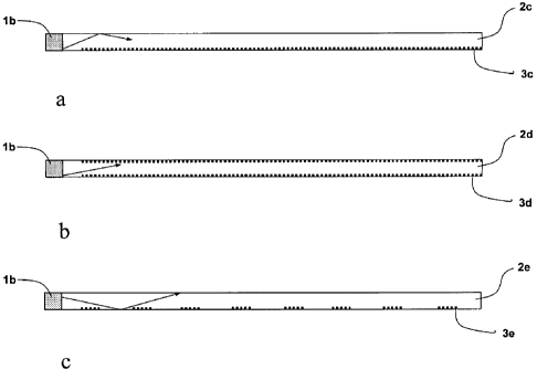
Fig. 2a illustrates an embodiment of an ultra thin lightguide element 2c
according to the
present invention with an optical surface relief structure 3c on one side of
the whole surface for
20 the light outcoupling. The lightguide element includes one lightguide
layer. This ultra thin
lightguide solution has a substantially even thickness typically about 0.25 to
about 0.4 mm with
the LED lb at the same height.
CA 02579217 2006-10-27
WO 2005/107363
PCT/1B2005/002334
21
Fig. 2b illustrates another embodiment of an ultra thin lightguide element 2d
according to
the present invention that includes an optical surface relief structure 3d on
both side of the whole
surface for the light outcoupling. This embodiment of an ultra thin lightguide
has a substantially
even thickness, typically about 0.25 to about 0.4 mm with the LED lb at the
same height.
Fig. 2c illustrates another embodiment of an ultra thin lightguide element 2e
according to
the present invention that includes an optical surface relief structure 3e on
one side of the surface
for the discrete light outcoupling. This ultra thin lightguide solution has a
substantially even
thickness, typically about 0.25 to about 0.4 mm with the LED lb at the same
height. This is a
suitable solution for the keypad or keyboard lighting.
Fig. 3 illustrates another embodiment of an ultra thin lightguide element 2f
according to
the present invention that includes an optical surface relief structure 3f on
at least one side of the
whole surface for the light outcoupling. This ultra thin lightguide solution
has a substantially
even thickness, typically about 0.25 to about 0.4 mm with an optical wedge
type adapter 4a for
better light incoupling into the lightguide. Along these lines, the LED lc may
have a height of
about 0.8 mm, while the lightguide element may have a thickness of about 0.2
mm. This
embodiment of an incoupling structure may include specular reflectors on the
top and bottom,
which can prevent any light loss and to improve incoupling efficiency.
Fig. 4a illustrates an embodiment of a curved ultra thin lightguide element 2g
according
to the present invention that includes an optical surface relief structure 3g
on at least one side of
the surface for light outcoupling. This embodiment of an ultra thin lightguide
can be flexible and
CA 02579217 2006-10-27
WO 2005/107363
PCT/1B2005/002334
22
curved into a preferred form in order to fulfill the total reflection theory,
and does not exceed the
total reflection angle. This ultra thin lightguide solution can utilize top
view LEDs Id.
Fig. 4b illustrates an embodiment of a double curved ultra thin lightguide
element 2h
according to the present invention with an optical surface relief structure 3h
on at least one side
of the surface for light outcoupling. This ultra thin lightguide can be
flexible and curved into a
preferred form in order to fulfill total reflection theory, and does not
exceed the total reflection
angle. This ultra thin lightguide solution may include at least two light
incoupling surfaces
utilizing top view LEDs id.
Fig. 5a illustrates an embodiment of an ultra thin flexible lightguide element
2i according
to the present invention including an arrangement for a larger matrix solution
with an optical
surface relief structure 3i on at least one side of the surface the light
outcoupling. This matrix
includes several lightguide modules in order to form larger illuminated active
area in at least one
direction. This application may be suitable backlight solution for a flat
display, such as an LCD
TV. This solution may include top view LEDs le as a light source. Of course,
other light
sources could be utilized and/or alternatively arranged, as may the lightguide
elements be
alternatively arranged.
Fig. 5b illustrates an embodiment of a flexible ultra thin lightguide element
2j according
to the present invention having two separate optical surface relief structures
3j at least a portion
of two different surfaces of the lightguide layer for light outcoupling. This
ultra thin lightguide
is flexible and can be bent into a desired form. Typically, the bending is
carried out in order to
CA 02579217 2006-10-27
WO 2005/107363
PCT/1B2005/002334
23
fulfill total reflection theory and does not exceed the total reflection
angle. This embodiment of
an ultra thin lightguide solution can utilize, for example top view LEDs 1d.
Fig. 6a illustrates an embodiment of a multi-layer lightguide element stack up
5a that is
based on two lightguide layers 2'k and 2"k with an optical surface relief
structure 3k on one side
of both layers on the whole surface for the light outcoupling. This lightguide
solution has
substantially even thickness typically about 0.4 to about 0.8 mm with the LED
if at the same
height.
Fig. 6b illustrates another embodiment of a multi-layer lightguide element
stack up 5b
that includes two lightguide layers 2' and 2" with an optical surface relief
structure 31 on one
side of both layer on the whole surface for the light outcoupling. This
lightguide solution has a
substantially even thickness typically about 0.4 to about 0.8 mm with the LED
if at the same
height.
Fig. 6c illustrates an embodiment of a multi-layer lightguide element stack up
5c that is
based on two lightguide layers 2'm and 2"m with an optical surface relief
structure 3'm and
3"m on both sides of both layers on the whole surface for the light
outcoupling. This lightguide
solution has a substantially uniform thickness typically about 0.4 to about
0.8 mm with the LED
if at the same height.
Fig. 6d illustrates an embodiment of a multi-layer dual lightguide element
stack up 5d
that includes two lightguide layers 2'k and 2"k with an optical surface relief
structure 3k on both
CA 02579217 2006-10-27
WO 2005/107363
PCT/1B2005/002334
, 24
side of both layers on the whole surface for the light outcoupling. Between
the lightguide layers
is placed one reflector film 6. This lightguide solution has a substantially
uniform thickness
typically about 0.4 to about 0.8 mm with the LED if at the same height.
Fig. 7a illustrates embodiments of the present invention that include
different multi-layer
lightguide element stack ups 5e, 5f, and 5g that include two lightguide layers
2'k, 2"k, 2'1, 2"1,
and 2'o, 2"o with an optical surface relief structure 3k, 31, and 3o on one
side of both layers on
the whole surface for the light outcoupling. Optical surface relief structure
can be diffractive
(binary or blaze) or refractive.
Fig. 7b illustrates embodiments of the present invention that include
different multi-layer
lightguide element stack ups 5h, 5i, and 5j that are based on two lightguide
layers 2'p, 2"p, 2'q,
2"q, and 2'r, 2"r with optical surface relief structures 3'p, 3"p, 3'q, 3"q,
and 3'r, 3"r on both
sides of both layer on whole surface for the light outcoupling. Optical
surface relief structure
can be diffractive (binary or blaze) or refractive.
Fig. 7c illustrates embodiments of the present invention that include
different multi-layer
lightguide element stack ups 5k, 51, and 5m that include two lightguide layers
2'k, 2"k and 2'1,
2"1 with an optical surface relief structure 3k and 31 on one side of both
layers on the whole
surface for the light outcoupling. Between the lightguide layers is placed one
reflector film 6 or
another type of optical film as prismatic film 7. The optical surface relief
structure can be
diffractive (binary or blaze) or refractive.
CA 02579217 2006-10-27
WO 2005/107363
PCT/1B2005/002334
Fig. 8a illustrates embodiments of a multi-layer dual lightguide element stack
up that
includes two lightguide layers 2's and 2"s having an optical surface relief
structure 3s on one
side of both layers on the whole surface for the light outcoupling. Between
the lightguide layers
is arranged a reflector film 6. The light incoupling and brightness may be
controlled by differing
5 thickness of lightguide layer, more thickness = more light, less
thickness = less light. This
lightguide solution is suitable for dual display backlighting, which has a
substantially uniform
thickness typically about 0.4 to about 0.8 mm with the LED 1 g at the same
height.
Fig. 8b illustrates embodiments of the present invention that include a multi-
layer
10 lightguide element stack up that includes two lightguide layers 2't and
2"t. The lightguide
layers have different cross-sectional areas. Optical surface relief structures
3't and 3"t are
provided on one side of both layers for the light outcoupling. As can be seen
in Fig. 8b, the
relief structures are arranged in different regions on each lightguide layer.
For example, the
lightguide layer 2't includes a relief structure over most if not all of its
surface. On the other
15 hand, the lightguide layer 21 includes relief structures in isolated
regions. This embodiment
could be utilized with a mobile phone that includes a display and a keypad.
Between the
lightguide layers is arranged a reflector film 6. The light incoupling and
brightness may be
controlled by differing thickness of lightguide layer, more thickness = more
light, less thickness
= less light. This lightguide solution is suitable for display backlighting
and keypad lighting,
20 which has a substantially uniform thickness typically about 0.4 to about
0.8 mm with the LED lg
at the same height.
Fig. 8c illustrates an embodiment of the present invention that includes a
multi-layer
CA 02579217 2006-10-27
WO 2005/107363
PCT/1B2005/002334
26
lightguide element stack up that includes three lightguide layers 2'u, 2"u,
and 2"u with optical
surface relief structure 3'u and 3"u on one side of each layer for the light
outcoupling. Between
the lightguide layers may be arranged reflector films 6. The light incoupling
and brightness may
be controlled by differing thickness of lightguide layer, more thickness =
more light, less
thickness = less light. This lightguide solution may be suitable for dual
display backlighting and
keypad lighting, which may have a substantially uniform thickness typically
about 0.4 ¨ 0.8 mm
with the LED 1g at the same height.
Fig. 9a illustrates an embodiment of the present invention that includes a
flexible multi-
layer dual lightguide element stack up that includes two lightguide layers 2'v
and 2"v with
optical surface relief structures 3'v and 3"v on at least a portion of a side
of both layers for the
light outcoupling. Between the lightguide layers may be arranged a reflector
film 6. This
lightguide solution is flexible and can be bent into a preferred form in order
to fulfill total
reflection theory and typically does not exceed total reflection angle. The
light incoupling and
brightness may be controlled by differing thickness of lightguide layer, more
thickness = more
light, less thickness = less light. This lightguide solution may be suitable
for dual display
backlighting, such as in a clam shell mobile phone, or flip phone, and may
have a substantially
uniform thickness, typically about 0.4 to about 0.8 mm with the LED lh at the
same height.
Fig. 9b illustrates an embodiment of the present invention that includes a
multi-layer
lightguide element stack up that is based on one lightguide layer 2w that
includes optical surface
relief structures 3w on one side of layer for the light outcoupling. The
lightguide layer is folded
up in order to form complete lightguide stack up. As can be seen in Fig. 9b,
the surface that
CA 02579217 2006-10-27
WO 2005/107363
PCT/1B2005/002334
27
includes the surface relief structures will contact itself. This illustrates
how the present invention
can provide a multilayer lightguide element with only one lightguide layer.
This lightguide
solution can prevent light leakage in the end of lightguide. The thickness is
typically about 0.2
to about 0.8 mm with the LED li at the same height.
Fig. 9c illustrates an embodiment of the present invention that includes a
multi-layer
lightguide element stack up that includes one lightguide layer 2w with an
optical surface relief
structure 3w on one side of layer for the light outcoupling. The lightguide
layer may be folded
up in order to form complete lightguide stack up. Between the lightguide
layers may be arranged
a reflector film 6. This lightguide solution can prevent light leakage in the
end of lightguide.
The thickness may typically be about 0.2 to about 0.8 mm with the LED li
having substantially
the height. The LED may be connected easily to the lightguide edge with
specific adapter, where
LED is in-molded.
Fig.1 Oa illustrates an embodiment of an ultra thin lightguide element 2y that
includes an
optical surface relief structure 3y on at least one side of the whole surface
for the light
outcoupling. The optical design 9, in the first part or light incoupling part
in the vicinity of the
light sources, may be optimized in such a manner that the light from the point
source lj:1, 1j:11,
1J:111 is diffused at different conical angles or directed partially at the
same angle, in order to
achieve more uniform and/or directed light distribution in the first part and
in the whole active
area divided for sectors 10:I, 10:II, 10:III per light source. The optic
design 9 is placed on the
top and the bottom surface of the first part of lightguide layer, having
diffractive or refractive
grooves. This embodiment of a lightguide element may not be dependent on
precise light source
CA 02579217 2006-10-27
WO 2005/107363
PCT/1B2005/002334
28
placement. This type of optical design can allow the use of different amounts
of light sources,
while having the minimum quantity of light sources and maximum quantity of
light sources on
the same edge, in order to achieve higher or lower brightness with the same
uniformity
performance.
Fig.10b illustrates an embodiment of an ultra thin lightguide 2y according to
the present
invention including an optical surface relief structure 3y on at least one
side of the whole surface
for the light outcoupling. The optical design 9, in the first part or light
incoupling part, of the
lightguide structure, may be optimized in such a manner that the light from
the point source lj:1,
lj:11, lj:111, 1 j:IV, lj:V is diffused at different conical angles or
directed partially at the same
angle, in order to achieve more uniform and/or directed light distribution in
the first part and in
the whole active area (divided for sectors 10:1, 10:II, 10:III, 10:1V, 10:V
per light source). The
optic design 9 may be placed on the top and the bottom surface of the first
part of lightguide
layer, having diffractive or refractive grooves. This lightguide type may not
be dependent on
precise light source placement. This type of optical design can allow the use
of different
amounts of light sources, while having the minimum quantity of light sources
and maximum
quantity of light sources on the same edge, in order to achieve higher or
lower brightness with
the same uniformity performance.
Fig.11 illustrates an embodiment of an ultra thin lightguide 2y having an
optical surface
relief structure 3y on at least one side of the whole surface for the light
outcoupling. The optical
outcoupling structure may be optimised with or without light incoupling
structure 9, which can
allow cutting and using the same lightguide design in different sizes 11a, 1lb
in order achieve
CA 02579217 2006-10-27
WO 2005/107363
PCT/1B2005/002334
29
the same uniformity performance. This can make lightguide solutions more
variable and flexible
to utilise it in different solutions and applications, without the need to
design many lightguides,
which have only slight differences in brightness and size requirements.
Fig.12a illustrates an embodiment of an ultra thin lightguide 2z:0, 2z:1 with
different
optical surface relief structures 3z:0, 3z:1 on at least one side of the whole
surface in order to
achieve different light performances such as light directing or collimating,
diverging, polarizing,
among others. The lightguide layer may be folded up in order to form complete
lightguide stack
up. This solution provides more performances in one package.
Fig.12b illustrates an embodiment of an ultra thin lightguide element 2z:0,
2z:1, 2z:2
having different optical surface relief structures 3z:0, 3z:1, 3z:2 on at
least one side of the whole
surface in order to achieve different light performances such as light
directing or collimating,
diverging, polarizing, among others. The lightguide layer may be folded up in
order to form
complete lightguide stack up. This solution can provide more performances in
one package.
Fig.13 illustrates an embodiment of an ultra thin lightguide 2z:0, 2z:1, 2z:2,
2z:3, 2z:4
with different an optical surface relief structures 3z:0, 3z:1, 3z:2, 3z:3,
3z:4 on at least one side
of the whole surface in order to achieve different light performances such as
light directing or
collimating, diverging, polarizing, among others. The lightguide layer may be
folded up in order
to form complete lightguide stack up. This solution can provide more
performances in one
package.
CA 02579217 2006-10-27
WO 2005/107363
PCT/1B2005/002334
Fig.14 illustrates an embodiment of a process for ultra thin lightguide
manufacturing by
means of continuous roll replication, also known as roll-to-roll. The material
moves from roll 12
to roll 14. Using this fast, cost-effective manufacturing method, bulk
material 13, such as
optically clear plastic film, such as PMMA, PC, or PET, can be replicated with
a surface relief
5 replicator 15 such as nickel coated cylinder, drum, roll having an
optical surface relief structure.
Fig. 15 illustrates another embodiment of a process for ultra thin lightguide
manufacturing by means of continuous roll replication, also known as roll-to-
roll. The material
moves from roll 12 to roll 14. Using this fast, cost-effective manufacturing
method, bulk
10 material 13, such as optically clear plastic film, such as PMMA, PC, or
PET, can be replicated
with a surface relief replicator 15 such as nickel coated cylinder, drum, roll
having an optical
surface relief structure. Additionally, other functional film 18, such as
reflector film, can be
laminated onto the surface of lightguide from the roll 17 during the same roll
to roll production
method. An extra pre-heating 16 may be suitable to utilize to achieve better
lamination quality.
Fig. 16 illustrates an embodiment of a process for ultra thin lightguide 21
manufacturing
by means of UV-casting. Using this fast, cost-effective manufacturing method
bulk material 21,
such as optically clear plastic resin, can be UV-cured with UV-light source 19
through the top
glass 20. An optical surface relief structure may be replicated in a mold 23
with a nickel plate 22
having a surface relief structure.
Fig. 17a illustrates an embodiment of a lightguide structures that may be
utilized in
regions of the lightguide element remote from light source(s). As shown in
this exemplary
CA 02579217 2006-10-27
WO 2005/107363
PCT/1B2005/002334
31
embodiment, the surface relief may include basic structural features, such as
grooves and/or
recesses arranged in different groups having different sizes, shapes,
orientations, configurations.
The characteristics of the surface relief may also vary. Along these lines,
the filling factor,
shape, size, profile, cross-section, and orientation, among other
characteristics. The groups may
or may not be arranged in repeating patterns. Each group may have any shape,
such as a regular
or irregular polygon. For example, the groups could be rectangular,
triangular, square,
trapezpoidal or any other shape. The arrangment of the grooves and/or recesses
may vary within
each sub-group, within each group, and/or over the entire structure. The
characteristics of the
grooves and their arrangement may vary be varied to vary the incoupling and/or
outcoupling
characteristics of the structure. For example, the arrangement could maximize
the diffraction
efficiency. The arrangement could also make diffraction efficiency is a
function of location. In
the embodiment shown in Fig. 17a, the surface relief structure is arranged in
groups 25. Each
group includes a plurality of sub-groups 27 that each include basic structural
features 26 on the
order of about 10 microns or less in height, and on the order of about 10
microns or less in each
lateral dimension. Each group and subgroup could have other configurations.
Fig. 17b illustrates an embodiment of a lightguide layer in the vicinity of
light source(s)
according to the present invention. In the embodiment shown in Fig. 17b, the
surface relief
structure is arranged in groups 29 in a regular pattern.
Fig. 17c illustrates an embodiment of a lightguide layer in the vicinity of
light source(s)
according to the present invention. In the embodiment shown in Fig. 17c, the
surface relief
structures are arranged in groups 29 in a non-regular pattern.
CA 02579217 2006-10-27
WO 2005/107363
PCT/1B2005/002334
32
Fig. 18 illustrates an embodiment of an ultra thin lightguide layer 2A for
keypad lighting.
This embodiment of the lightguide element has a thickness of about 50 to about
200 microns,
which provides a good flexible and touch sensitive performances retaining a
click effect. The
lightguide layer is arranged placed between keypad 30 and dome sheet 32 and
utilize much less
space than a conventional lightguide. Due to the thin and flexible nature of
the lightguide layer,
the keypad pressing can make electrical contact between dome sheet and the
circuit board 33.
The discrete optic surface relief structure of light outcoupling 3A is
preferable fine grating
structure. The grating structures may be optimized in order to achieve high
outcoupling
efficiency in 00 angle (collimated light). The keypad is diffusing collimated
light for larger
illumination angle.
Fig. 19a illustrates an embodiment of an ultra thin lightguide layer 2'a for
keypad
lighting with the fine optic surface relief structures 3'a provided over the
whole surface to form a
uniform illuminating area.
Fig. 19b illustrates an embodiment of an ultra thin lightguide layer 2"a that
may be
utilized with for keypad lighting with the discrete fine optic surface relief
structures 3"a forming
uniform and discrete illuminating areas.
Fig. 19c illustrates an embodiment of an ultra thin lightguide layer 2"ä for
keypad
lighting with the fine optic surface relief structures 3"'a, and short
boundary surface lines 34
produced by cutting process, which can be reflecting or directing light for
the illuminating areas.
CA 02579217 2006-10-27
WO 2005/107363
PCT/1B2005/002334
33
Fig. 20a and 20b illustrate, respectively, an overhead view and a side view of
an
embodiment of a lighting element 26 with an improved light incoupling using a
bundle of split
optic fibers 35 between light source lk and the lightguide layer.
Fig. 21a illustrates embodiment of an ultra thin lightguide element 21
according to teh
present invention wherein the surface relief structures are arranged in small
discrete outcoupling
structure groups 29, wherein a region 36' of the lightguide layer in the
vicinity of the at least one
longitudinal light source 11 the outcoupling structure groups include about
10% or less of the
area of the lightguide layer.
Fig. 2 lb illustrates embodiment of an ultra thin lightguide element 2"d.
according to the
present invention wherein the surface relief structures are arranged in small
discrete outcoupling
structure groups 29, wherein a region 36" of the lightguide layer in the
vicinity of the at least
one point light source lm, the outcoupling structure groups include about 10%
or less of the area
of the lightguide layer. The maximum distance D between small discrete
outcoupling structure
groups is 300 microns or less.
Fig. 22 illustrates embodiment of small portion of ultra thin lightguide layer
2d wherein
the basic structural features 26 of surface relief structures is forming a
small discrete outcoupling
structure group 29.
Fig. 23 illustrates embodiment of small portion of ultra thin lightguide layer
Td wherein
CA 02579217 2006-10-27
WO 2005/107363
PCT/1B2005/002334
34
the different basic structural features 26 of surface relief structures are
forming small discrete
outcoupling structure groups 29, wherein the number, arrangement and size of
each surface relief
structure and height and lateral dimensions of the structural features of the
surface relief
structures being varied to provide a desired degree of outcoupling modulation
of light incoupled
into the light guide element.
The embodiments illustrated and discussed in this specification are intended
only to teach
those skilled in the art the best way known to the inventors to make and use
the invention.
Nothing in this specification should be considered as limiting the scope of
the present invention.
All examples presented are representative and non-limiting. The above-
described embodiments
of the invention may be modified or varied, without departing from the
invention, as appreciated
by those skilled in the art in light of the above teachings. It is therefore
to be understood that,
within the scope of the claims and their equivalents, the invention may be
practiced otherwise
than as specifically described.