Note: Descriptions are shown in the official language in which they were submitted.
CA 02579377 2007-03-02
WO 2006/028316 PCT/KR2004/003313
METHOD FOR IMPROVEMENT OF PERFORMANCE OF SI
THIN FILM ANODE FOR LITHIUM RECHARGEABLE BATTERY
FIELD OF THE INVENTION
The present invention relates to a method for improving charge/discharge
cycle characteristics of a lithium secondary battery using a Si based anode
active
material. More specifically, the present invention relates to a method for
improving
charge/discharge characteristics of a lithium secondary battery by surface-
treating a
surface of an anode current collector to have specific morphology, and
preferably
vapor-depositing a silicon film, as the anode active material by sputtering
under
application of bias voltage to the surface-treated anode current collector,
and/or
disposing an adhesive layer between the surface-treated anode current
collector and
silicon film, so as to reinforce bondability between the anode current
collector and
active material, ultimately leading to improvement of charge/discharge cycle
characteristics of the battery.
BACKGROUND OF THE INVENTION
Technological development and increased demand for mobile instruments has
lead to a rapid increase in the demand for secondary batteries as an energy
source.
Among these secondary batteries, a great deal of research and study has been
focused
on a lithium secondary battery having high energy density and discharge
voltage and
-1-
CA 02579377 2007-03-02
WO 2006/028316 PCT/KR2004/003313
thus such lithium secondary batteries have been commercialized and entered
wide use.
Recently, a great deal of attention has been directed to the lithium secondary
battery using a Li-Si based active material as the anode. Pure silicon (Si)
has
theoretical specific capacity of 4200 mAh/g that is significantly greater than
372 mAh/g
of graphite carbon. However, Si undergoes significant changes in volume
thereof over
continuous charge/discharge cycles, which causes mechanical and electrical
degradation, and thus such poor charge/discharge cycle characteristics have
been
raised as the point at issue.
An attempt to solve such problems associated with charge/discharge cycle
characteristics, some conventional arts have proposed a novel configuration of
the
electrode in which a surface of a copper current collector is made rough and
an
amorphous silicon film is vapor-deposited thereon. Such an electrode exhibits
high
reversible capacity of greater than 3000 mAh/g, but three still remains a need
for
further improvement of charge/discharge cycle characteristics thereof.
The reason of capacity decrease occurring in the course of the
charge/discharge cycle is generally known to be due to loss of electrical
contact
between the silicon film and current collector. Therefore, if a method for
improving
electrical contact between the silicon film and current collector in the
lithium
secondary battery made up of the Li-Si based anode could be developed, it will
be
possible to manufacture a lithium secondary battery having excellent
charge/discharge
cycle characteristics.
SUMMARY OF THE INVENTION
Therefore, the present invention has been made in view of the above
-2-
CA 02579377 2007-03-02
WO 2006/028316 PCT/KR2004/003313
problems, and it is an object of the present invention to provide a method for
improving charge/discharge cycle characteristics of a lithium secondary
battery using
a Si based anode active material.
The present inventors have conducted a variety of extensive and intensive
study and experimentation to solve the most important problem as described
above, that
is, loss of electrical contact between a silicon film and anode current
collector when
charging/discharging, exhibited by the lithium secondary battery including the
Si based
anode active material. As a result of such extensive investigation, the
inventors have
found that when the anode current collector is treated to have specific
surface
morphology, the problem of electrical contact loss can be greatly improved,
and further
found that it is possible to remarkably improve charge/discharge cycle
characteristics
of the battery by applying bias voltage to the current collector, in the
course of vapor-
depositing the silicon film on the surface-treated anode current collector by
sputtering,
and/or disposing an adhesive layer between the anode current collector and
silicon
film. The present invention has been completed based on these findings.
Therefore, in the lithium secondary battery using the Si based anode active
material, the method for improving charge/discharge cycle characteristics of
the
battery in accordance with the present invention comprises surface-treating
the anode
current collector such that the surface morphology of the anode current
collector has
grain boundaries of 5 to 100 m in size throughout the entire surface of the
anode
current collector, and trenches having a depth of more than 1 m formed at
grain
boundary junctions.
BRIEF DESCRIPTION OF THE DRAWINGS
-3-
CA 02579377 2007-03-02
WO 2006/028316 PCT/KR2004/003313
The above and other objects, features and other advantages of the present
invention will be more clearly understood from the following detailed
description
taken in conjunction with the accompanying drawings, in which:
Figs. 1 and 2 are, respectively, SEMs for a surface and vertical cross section
of a silicon thin film vapor-deposited on a Si-wafer by sputtering, in Example
2;
Figs. 3 and 4 are, respectively, SEMs for surface and vertical cross section
of
a silicon thin film vapor-deposited on a Si-wafer by applying bias voltage
upon
sputtering, in Example 2;
Figs. 5 and 6 are, respectively, SEMs for surface of a silicon thin film vapor-
deposited on a Ni foil, in Example 2;
Figs. 7 and 8 are, respectively, graphs showing charge/discharge profiles of a
lithium secondary battery, in Example 2;
Figs. 9 through 12 are, respectively, SEMs for surfaces of Cu foils, in
Example 3 and Comparative Examples 1 through 3;
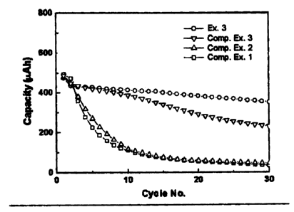
Fig. 13 is a graph showing charge/discharge cycle characteristics of lithium
secondary batteries prepared in Example 3 and Comparative Examples 1 through
3;
Fig. 14 is a graph showing charge/discharge cycle characteristics of a lithium
secondary battery, in Example 4;
Figs. 15 and 16 are, respectively, SEMs for surface of a silicon thin film,
after
1 and 18 times of charge/discharge cycles in Example 4; and
Figs. 17 and 18 are, respectively, SEMs for surface of a silicon thin film,
after
1 and 18 charge/discharge cycles in Example 3.
-4-
CA 02579377 2007-03-02
WO 2006/028316 PCT/KR2004/003313
DETAILED DESCRIPTION OF THE INVENTION
The present inventors have confirmed through extensive experimentation that
the anode current collector having the above-mentioned surface morphology
provides,
when vapor-depositing a silicon film on the surface thereof, remarkably
increased
adhesiveness between the silicon film and anode current collector, and thus
exhibits
minimal loss of electrical contact therebetween even though the silicon film,
as the
anode active material, undergoes significant changes in volume thereof, upon
charging/discharging.
The anode current collector is fabricated to have a thickness of about 3 to
500
m. There is no particular limit to anode current collectors, so long as they
have
conductivity without causing chemical changes in the battery of interest. As
examples of anode current collectors, mention may be made of copper, nickel,
stainless steel, aluminum, titanium, sintered carbon, copper or stainless
steel surface-
treated with carbon, nickel, titanium or silver, and an aluminum-cadmium
alloy.
Preferably, copper, nickel or stainless steel may be used as the anode current
collector.
The anode current collector may be used in various forms including films,
sheets,
foils, nets, porous structures, foams and non-woven fabrics.
Even though a method is known in the art of forming micro irregularities by
surface-treating the surface of the anode current collector, there is no known
example
of improving charge/discharge cycle characteristics of the Si based anode
active
material by forming specific surface morphology as in the present invention.
Further, when failing to obtain the surface morphology as achieved in the
present
invention, in spite of surface treatment to form micro irregularities
according to
conventional arts, it can be confirmed through the following Examples and
-5-
CA 02579377 2007-03-02
WO 2006/028316 PCT/KR2004/003313
Comparative Examples that charge/discharge cycle characteristics of the anode
active
material were deteriorated.
Preferably, the Si based anode active material may be amorphous silicon or
nano crystalline silicon. In addition, in order to alleviate volume expansion
of Si
itself and improve electrical conductivity of silicon, other elements may be
added to
prepare the anode active material in the form of an alloy. As elements that
can be
added, mention may be made of for example, zirconium (Zr), titanium (Ti), iron
(Fe),
vanadium (V), cobalt (Co), nickel (Ni), copper (Cu), chromium (Cr), manganese
(Mn), molybdenum (Mo), tantalum (Ta), tungsten (W), tin (Sn), silver (Ag) and
aluminum (Al), which may used alone or in any combination thereof.
The size of the grain boundaries in the present invention is within the range
of
5 to 100 m, as described above. If the size of the grain boundaries is too
small, this
results in difficulty to induce formation of self-organized micro columnar
structures
through the grain boundaries, and thereby difficulty to disperse stress due to
volume
expansion of the anode active material resulting from a reaction of Li with
Si. In
contrast, if the size of the grain boundaries is too large, this may
undesirably lead to
deterioration of dispersion and alleviation effects of stress in the grain
boundaries
formed in a large size when the vapor-deposited anode active material reacts
with Li.
In addition, the depth of trenches formed at the grain boundary junctions is
greater than 1 m, as described above. Where the depth of trenches is too
shallow,
this may undesirably lead to difficulty to induce cracking along trenches
formed at the
grain boundary junctions or difficulty to induce formation of self-organized
micro
columnar structure through the grain boundaries, in formation of cracks due to
volume
expansion of Si resulting from a reaction of Li and Si.
-6-
CA 02579377 2007-03-02
WO 2006/028316 PCT/KR2004/003313
Various processes may perform the surface treatment of forming the above-
mentioned specific morphology on the anode current collector surface. For
example,
mention may be made of chemical or electrical etching by a wet method, and
reactive
gas or ion etching by a dry method.
As an example, for performing chemical etching, when Cu or Ni is used as the
anode current collector, a mixture of FeC13/HCl/H2O in the ratio of 1: 8.5 :
33.7
(volume percent) is preferably used as an etchant. Etching time may vary
depending
upon various factors including kinds of anode current collectors and etchants,
and thus
may determined under conditions capable of forming the above-mentioned surface
morphology, taking into account such factors.
An anode for the lithium secondary battery is prepared by vapor-depositing
the silicon film, as the active material, on the anode current collector
having such a
surface morphology. Methods of vapor-depositing the silicon film include, but
are
not limited to, sputtering, LPCVD (Low Pressure Chemical Vapor Deposition),
PECVD (Plasma Enhanced Chemical Vapor Deposition) and vacuum evaporation, for
example. Preferably, sputtering may be used. The thickness of the silicon film
is
preferably within the range of 0.5 to 10 m, in order to ensure suitable
function as the
anode active material.
As a preferred embodiment, when the silicon film is vapor deposited by
sputtering, bias voltage may be applied to the anode current collector to
further
improve bondability between the silicon film and anode current collector. The
bias
voltage is preferably within the range of between about -25 V and -200 V.
Increased adhesiveness of the silicon film to the anode current collector by
application of bias voltage upon sputtering may correlate with an enhanced
-7-
CA 02579377 2007-03-02
WO 2006/028316 PCT/KR2004/003313
intermixing reaction between the silicon film and anode current collector due
to
bombardment of energetic ions during sputtering under application of bias
voltage.
As another preferred example, the anode structure may further comprise an
adhesive layer on the interface between the silicon film and anode current
collector.
There is no particular limit to the thickness of the adhesive layer, so long
as it does not
have detrimental effects on functions of the anode. Preferably, the thickness
of the
adhesive layer is in the range of about 50 to 500A.
The present inventors have confirmed through extensive experimentation that
the lithium secondary battery, which was configured using the anode having the
adhesive layer disposed between the surface-treated anode current collector,
as
described above, and silicon film, forms unique surface morphology on the
silicon
film after several charge/discharge cycles. This is specifically illustrated
in Example
4, which follows, and it is believed that such a phenomenon significantly
improves
charge/discharge cycle characteristics.
The adhesive layer is made of material having excellent chemical affinity for
components of both the silicon film and anode current collector, without
affecting
anode functions. For example, when Cu or Ni is utilized as the anode current
collector, the adhesive layer is particularly preferably a zirconium thin
film.
As described above, the present invention achieves improving
charge/discharge characteristics of a lithium secondary battery, comprising
(a)
surface-treating a surface of an anode current collector to form specific
surface
morphology, (b) preferably, applying bias voltage to the anode current
collector when
a silicon film is vapor-deposited on the surface-treated anode current
collector by
sputtering, or (c) forming an adhesive layer between the anode current
collector and
-8-
CA 02579377 2007-03-02
WO 2006/028316 PCT/KR2004/003313
silicon film, so as to reinforce bondability between the silicon film and
anode current
collector, thus ultimately leading to improvement of charge/discharge cycle
characteristics. However, it is true, of course, that better effects desired
in the
present invention can be achieved when all of the above-mentioned three
requirements
are satisfied.
If necessary, heat treatment may be performed to further enhance
bondability between the anode current collector and adhesive layer, after
formation of
the adhesive layer on the anode current collector. The heat treatment induces
interface reaction between the anode current collector and adhesive layer,
whereby
some ingredients of the anode current collector diffuse to the adhesive layer
and
conversely, some ingredients of the adhesive layer diffuse to the anode
current
collector, resulting in enhanced affinity leading to increased bondability.
The heat
treatment may be performed at a temperature of 100 to 400 C for 10 sec to 30
min, for
example.
In accordance with another aspect of the present invention, there is provided
a
lithium secondary battery comprising the anode treated or fabricated by the
above-
mentioned method, a cathode, a separator and a non-aqueous electrolyte
containing a
lithium salt.
The cathode is fabricated, for example, by applying a mixture of a cathode
active material, a conductive agent and a binding agent to the cathode current
collector, followed by drying. If necessary, a filling agent may be further
added to
the mixture.
The cathode current collector is generally fabricated to a thickness of 3 to
500
m. This cathode current collector is not particularly limited, so long as it
exhibits
-9-
CA 02579377 2007-03-02
WO 2006/028316 PCT/KR2004/003313
high conductivity without causing chemical changes in the concerned battery.
For
example, as the cathode current collector, mention may be made of stainless
steel,
aluminum, nickel, titanium, sintered carbon and, aluminum or stainless steel
surface
treated with carbon, nickel, titanium, silver, or the like. The current
collector may be
fabricated to have micro irregularities on the surface thereof so as to
enhance
adhesiveness to the cathode active material. In addition, the current
collector may be
made in various forms including films, sheets, foils, nets, porous structures,
foams and
non-woven fabrics.
Lithium transition metal oxides which can be used as the cathode active
material in the present invention include, but are not limited to, layer-like
compounds
such as lithium cobalt oxide (LiCoO2) and lithium nickel oxide (LiNiOZ) or
compounds substituted with one or more transition metal; lithium manganese
oxides
such as a compound which is represented by the Formula Li1+,,Mn2_XO4 wherein x
is
between 0 an 0.33, LiMnO3, LiMnZO3 and LiMnO2; lithium copper oxide (LiZCuO2);
vanadium oxides such as LiV3O8, LiFe3O4, V205 and Cu2V2O7; a Ni-site type
lithium
nickel oxide which is represented by Formula LiNil_XM,O2 wherein M is Co, Mn,
Al,
Cu, Fe, Mg, B or Ga, and x is between 0.01 and 0.3; lithium manganese
composite
oxides which are represented by Formula LiMn2_,,MXO2 wherein M is Co, Ni, Fe,
Cr, Zn
or Ta, and x is between 0.01 and 0.1, or Formula Li2Mn3MO8 wherein M is Fe,
Co, Ni,
Cu or Zn; LiMn2O4 wherein a part of Li is substituted with alkaline earth
metal ions;
disulfide compounds; and Fe2(Mo04)3.
The conductive agent utilized in the present invention is typically added in
an
amount of 1 to 50% by weight, based on the total weight of a mixture including
the
cathode active material. There is no particular limit to the conductive agent,
so long
as it has conductivity without causing chemical changes in the battery of
interest. As
-10-
CA 02579377 2007-03-02
WO 2006/028316 PCT/KR2004/003313
examples of conductive agents, mention may be made of graphite such as natural
or
artificial graphite; carbon blacks such as carbon black, acetylene black,
Ketjen black,
channel black, furnace black, lamp black and thermal black; conductive fibers
such as
carbon fibers and metal fibers; carbon fluoride; metal powder such as aluminum
or
nickel powder; conductive whiskers such as zinc oxide and potassium titanate;
conductive metal oxides such as titanium oxide; and conductive materials such
as
polyphenylene derivatives.
The binding agent is an ingredient assisting in bonding between the active
material and conductive agent, and in binding to current collectors. The
binding agent
utilized in the present invention is typically added in an amount of 1 to 50%
by weight,
based on the total weight of a mixture including cathode active material. As
examples
of the binding agent, mention may be made of polyfluorovinylidene, a polyvinyl
alcohol, carboxymethylcellulose (CMC), starch, hydroxypropylcellulose,
recycled
cellulose, polyvinyl pyrollidone, tetrafluoroethylene, polyethylene,
polypropylene, an
ethylene-propylene-diene terpolymer (EPDM), sulfonated EPDM, styrene butylene
rubber, fluoro rubber and various copolymers.
The filling agent is an ingredient that inhibits cathode expansion and is
optionally utilized. There is no particular limit to the filling agent, so
long as it does
not cause chemical changes in the battery of interest and is a fibrous
material. As
examples of the filling agent, there may be used olefin polymers such as
polyethylene
and polypropylene; and fibrous materials such as glass fiber and carbon fiber.
The separator is disposed between the anode and cathode. As the separator,
an insulating thin film having high ion permeability and mechanical strength
is used.
The separator typically has a pore diameter of 0.01 to 10 m and a thickness
of 5 to
-11-
CA 02579377 2007-03-02
WO 2006/028316 PCT/KR2004/003313
300 m. As separators that can be used in the present invention, mention may
be
made of olefin polymers such as chemically resistant and hydrophobic
polypropylene;
and sheets or non-woven fabrics made of glass fiber or polyethylene. When a
solid
electrolyte such as a polymer is employed as the electrolyte, the solid
electrolyte may
also serve as both the separator and electrolyte.
The non-aqueous electrolyte containing lithium salt is composed of a non-
aqueous electrolyte and lithium. As the non- aqueous electrolyte, a non-
aqueous
electrolyte solution, organic solid electrolyte and inorganic solid
electrolyte may be
utilized.
As the non-aqueous electrolyte solution, for example, mention may be made of
non-protic organic solvents such as N-methyl-2-pyrollidinone, propylene
carbonate,
ethylene carbonate, butylene carbonate, dimethyl carbonate, diethyl carbonate,
gamma-
butyro lactone, 1,2-dimethoxy ethane, tetrahydroxy Franc, 2-methyl
tetrahydrofuran,
dimethylsulfoxide, 1,3-dioxolane, formamide, dimethylformamide, dioxolane,
acetonitrile, nitromethane, methyl formate, methyl acetate, phosphoric
triester,
trimethoxy methane, dioxolane derivatives, sulfolane, methyl sulfolane, 1,3-
dimethyl-2-
imidazolidinone, propylene carbonate derivatives, tetrahydrofuran derivatives,
ether,
methyl propionate and ethyl propionate.
As examples of the organic solid electrolyte utilized in the present
invention,
mention may be made of polyethylene derivatives, polyethylene oxide
derivatives,
polypropylene oxide derivatives, phosphate polymers, poly agitation lysine,
polyester
sulfone, polyvinyl alcohol, poly(vinylidene fluoride), and polymers'
containing ionic
dissociation groups.
As examples of the inorganic solid electrolyte utilized in the present
invention,
-12-
CA 02579377 2007-03-02
WO 2006/028316 PCT/KR2004/003313
mention may be made of nitrides halides and sulphates of lithium such as Li3N,
LiI,
Li5NI2, Li3N-LiI-LiOH, LiSiO4, LiSiO4-LiI-LiOH, Li2SiS3, Li4SiO4, Li4SiO4-LiI-
LiOH
and Li3PO4-Li2S-SiS2.
The lithium salt is a material that is readily soluble in the non-aqueous
electrolyte and may include, for example, LiCI, LiBr, LiI, LiC1O4, LiBF4,
LiBIoClio,
LiPF6, LiCF3SO3, LiCF3CO2, LiAsF6, LiSbF6, LiAIC14, CH3SO3Li, CF3SO3Li,
(CF3SO2)2NLi, lithium chloroborate, lower aliphatic carboxylic acid lithium,
lithium
tetraphenyl borate and imide.
Additionally, in order to improve charge/discharge characteristics and flame
retardancy, for example, pyridine, triethylphosphite, triethanol amine, cyclic
ester,
ethylene diamine, n-glyme, hexamethylphosphoric triamide, nitrobenzene
derivatives,
sulfur, quinone-imine dye, n-substituted oxazolidinone, N,N-substituted
imidazolidine,
ethylene glycol dialkyl ether, ammonium salts, pyrrole, 2-methoxy ethanol,
aluminum
trichloride or the like may be added to the non-aqueous electrolyte. If
necessary, in
order to impart incombustibility, the non-aqueous electrolyte may further
contain
halogen-containing solvents such as carbon tetrachloride and ethylene
trifluoride. In
addition, the non-aqueous electrolyte may further contain carbon dioxide gas,
in order
to improve high temperature preservability.
As described above, illustrative description was provided on constitutive
components of the battery that can be configured using the aluminum based-
cathode
current collector in accordance with the present invention, but if necessary,
some of
constitutive components may be excluded or substituted or other constitutive
components may be further added.
-13-
CA 02579377 2007-03-02
WO 2006/028316 PCT/KR2004/003313
DESCRIPTION OF THE PREFERRED EMBODIMENTS
Now, the present invention will be described in more detail with reference to
the following Examples. These examples are provided only for illustrating the
present
invention and should not be construed as limiting the scope and sprit of the
present
invention.
Example 1
FeC13 was mixed to a final concentration of 0.4 M in an aqueous 2.4 M HCI
solution to prepare an etching solution that was then used in surface
treatment by
etching the surface of a Ni foil for about 1 min. On the surface treated-Ni
foil current
collector, a Si thin film of 5000 A thickness was formed from a Si target
having a
diameter of 2" (99.99%) by R.F. magnetron sputtering. Sputtering was performed
in a
chamber which had been vacuum pumped to 2 x 10'6 Torr and then set to 5 mTorr
by
injection of argon gas.
In order to confirm electrochemical properties of the Si thin film electrode,
two
#2016 coin cell batteries were prepared using a pure Li foil as a cathode, and
a mixed
solution in which 1 M LiPF6 was added to a mixed solvent of ethylene carbonate
(EC)
and diethylene carbonate (DEC) ( volume ratio 1:1), as an electrolyte
solution. These
cell batteries were assembled in a globe box under argon atmosphere, and were
then
subjected to more than 30 charge/discharge experiments at 0 to 1.2 V using
current of
100 A/cm2 at 30 C. Results thus obtained confirmed that the batteries
exhibited
excellent charge/discharge cycle characteristics.
-14-
CA 02579377 2007-03-02
WO 2006/028316 PCT/KR2004/003313
Example 2
In order to confirm effects due to application of bias voltage during
sputtering,
the following experiments were performed: Experiment A; vapor-deposition of a
Si thin
film on a Si-wafer by sputtering, and Experiment B; vapor-deposition of the Si
thin film
on the Si-wafer by sputtering while applying DC bias voltage of -100 V.
Figs. 1 and 2 show SEMs of the surface (Fig. 1) and vertical cross-section
(Fig.
2) of the Si thin film obtained in Experiment A, respectively. Figs. 3 and 4
show
SEMs of the surface (Fig. 3) and vertical cross-section (Fig. 4) of the Si
thin film
obtained in Experiment B, respectively.
The Si thin film in Experiment A revealed a columnar structure having rough
surface morphology and cross section, while the Si thin film in Experiment B
revealed a
smoother vapor-deposition surface due to application of bias voltage.
These Si thin films were subjected to charge/discharge experiments as in
Example 1. Fig. 5 shows an SEM of the surface of the Si thin film after one
charge/discharge cycle (Experiment A) and Fig. 7 is a graph showing the
charge/discharge profile thereof. Meanwhile, Fig. 6 shows an SEM of the
surface of
the Si thin film after one charge/discharge cycle (Experiment B) and Fig. 8 is
a graph
showing charge/discharge profile thereof. Comparing these results, the lithium
secondary battery utilizing the Si thin film in Experiment B exhibited
relatively low
initial irreversible capacity and relatively high charge/discharge cycle
characteristics, as
shown in Fig. 8. Surmising from SEMs in Figs. 5 and 6, it seems that such
results are
due mainly to increased adhesiveness of the Si thin film by application of
bias voltage.
-15-
CA 02579377 2007-03-02
WO 2006/028316 PCT/KR2004/003313
Example 3
Instead of a Ni foil, a Cu foil was surface-treated using the same procedure
as
in Example 1, and the experiment was repeated by applying DC bias voltage of -
100 V
using the same procedure as in Example 2.
Fig. 9 shows an SEM of the surface of the etched Cu foil, and Fig. 13 is a
graph showing charge/discharge cycle characteristics of the battery fabricated
using this
Cu foil.
Comparative Examples 1 - 3
Experiments were repeated using the same procedure as in Example 3, except
that etching was not performed (Comparative Example 1), or etching solutions
listed in
Table 1 below were used instead of the FeC13/HC1/HZO etching solution and
etching
time was varied (Comparative Examples 2 and 3).
[Table 1]
Etching Solution Etching Time SEM of Surface
Ex. 3 FeC13+HC1+H20 1 min Fig. 9
Comp. Ex. 1 - 0 Fig. 10
Comp. Ex. 2 HNO3+H20 3 min Fig. 11
Comp. Ex. 3 FeCl3+H20 5 min Fig. 12
Figs. 10 through 12 show SEMs of respective surfaces of the etched Cu foils.
It is noteworthy that the Cu foil in Example 3 exhibited surface morphology
(Fig. 9)
-16-
CA 02579377 2007-03-02
WO 2006/028316 PCT/KR2004/003313
significantly distinctive from those of Comparative Examples 1 through 3
(Figs. 10
through 12). That is, it was confirmed that the surface of the Cu foil in
Example 3
revealed relatively broadly and deeply developed grain boundaries.
Fig. 13 is a graph showing charge/discharge cycle characteristics of batteries
in Comparative Examples 1 through 3, together with results obtained in Example
3.
It can be seen from these results that charge/discharge cycle characteristics
of batteries
showed close relationship with surface morphology of the Cu base material, and
the
battery in Example 3 exhibited particularly excellent results.
Effects of surface roughness of the Cu base on improvement of
charge/discharge cycle characteristics were caused by formation of a micro
columnar
structure during charging/discharging of the battery. Relevant surface-
treatment of
the Cu base by etching provides a Si thin film having an excellent self-
organized
micro columnar structure, and thus reduces stress and tension caused by
changes in
volume during charge/discharge cycle of the battery. Therefore, as shown in
Fig. 13,
the battery in Example 3 exhibited excellent capacity preservability compared
to
batteries in Comparative Examples 1 through 3.
Example 4
The experiment was repeated using the same procedure as in Example 3,
except that, on the surface of the Cu foil etched in Example 3, a Si thin film
was vapor-
deposited following vapor-deposition of a Zr layer of 100 A thickness by
application of
DC bias voltage of -100 V to a substrate using R.F. magnetron sputtering.
-17-
CA 02579377 2007-03-02
WO 2006/028316 PCT/KR2004/003313
Fig. 14 is a graph showing charge/discharge cycle characteristics of the
battery prepared in Example 4, together with results obtained in the battery
of
Example 3. As can be seen from Fig. 14, interposition of the Zr layer between
the
Cu foil and Si thin film further improved charge/discharge cycle
characteristics of
battery.
Figs. 15 and 16 show, respectively, SEMs of the Si thin film, after 1 and 18
charge/discharge cycles in the battery of Example 4. In contrast with these
results,
Figs. 17 and 18 show, respectively, SEMs of the Si thin film, after 1 and 18
charge/discharge cycles in the battery of Example 3. Upon comparing Fig. 16
with
Fig. 18, it was confirmed that both electrodes in Examples 3 and 4 exhibited
formation
of cracks after 18 charge/discharge cycles, but there were significant
structural
differences therebetween. That is, Fig. 16 exhibited formation of wide gaps
along
grain boundary profile of the Cu base, as shown in Fig. 1 and also formation
of narrow
gaps within a plurality of islands surrounded by such wide gaps, thus showing
generally a structure in which micro islands having a small and uniform size
were
formed by narrow gap. The thus-formed micro columnar structure was proven to
be
stable during charge/discharge cycles, as shown in Fig. 14. This was possible
because interposition of the Zr layer, as the adhesive layer, between the Cu
current
collector and Si thin film strengthened adhesiveness of Si to the Cu base. In
comparison with this result, Fig. 18 exhibited randomized distribution of
islands and
cracks, and a structure of islands having a relatively larger size. Further,
it was also
confirmed that some islands were separated from the Cu base. Therefore, it can
be
seen that introduction of the Zr adhesive layer to the interface between the
Si thin film
and Cu base could completely resolve the problem associated with gradual
decrease of
battery capacity occurring during charge/discharge cycles.
-18-
CA 02579377 2007-03-02
WO 2006/028316 PCT/KR2004/003313
As described above, in accordance with the method of the present invention, it
is possible to prepare a lithium secondary battery having excellent
charge/discharge
cycle characteristics by reinforced bondability between the silicon film, as
the anode
active material and current collector, and thereby minimization of loss of
electrical
contact in the course of a charge/discharge process.
Although the preferred embodiments of the present invention have been
disclosed for illustrative purposes, those skilled in the art will appreciate
that various
modifications, additions and substitutions are possible, without departing
from the
scope and spirit of the invention as disclosed in the accompanying claims.
-19-