Note: Descriptions are shown in the official language in which they were submitted.
CA 02579697 2007-02-26
ELECTRONIC DEVICE TEST SET AND CONTACT USED THEREIN
Cross-Reference to Related Applications
This is a regular application filed under 35 U.S.C.
111(a) claiming priority, under 35 U.S.C. 119(e) (1), of
provisional application Serial No. 60/776,654, previously
filed February 24, 2006 under 35 U.S.C. 111(b).
Technical Field
The present invention relates broadly to the field of
testing of electronic devices such as integrated circuits.
More narrowly, however, the invention deals with test sets for
interfacing pads or leads of a device to be tested with
corresponding pads of a circuit board of a test apparatus. A
specific embodiment of the invention focuses upon the
construction and mounting of a contact of the test set.
Background of the Invention
The testing of integrated circuit devices is performed to
ensure that such devices, when sold to a customer, are of as
high a degree of quality as possible. Various types of test
apparatus have been utilized over the years to accomplish
testing. Typically, a tester includes a printed circuit board
which has defined thereon a plurality of conductive traces.
1
CA 02579697 2007-02-26
These traces on the circuit board, or load board, are
associated with corresponding functions of the test apparatus.
In order to accomplish testing, it is necessary to
interconnect a lead, in the case of a leaded device under
test, or a pad, of a nonleaded device under test, to a
corresponding trace on the load board. A test set or test
socket having a plurality of contacts is interposed between
the device under test and the load board in order to
effectuate interconnection. A contact is engaged, at an upper
end thereof, by the lead or pad of the DUT, depending upon the
type of DUT being tested, with its corresponding trace on the
load board. A lower end of the contact is in engagement with a
trace on the load board.
As technology has progressed, the size, shape and
electronic properties of contacts have evolved in response to
the construction of test sets and load boards and the
architecture of devices to be tested. At one time, it was
considered necessary to have a wiping action at the various
locations of engagement of the contact ends by the lead or pad
of the DUT and the pad on the load board. Such wiping action
was deemed to facilitate a good transmission path through the
contact because of a good connection at either end thereof. It
has become more apparent, however, that the measure of wiping
action formerly considered necessary to maintain a good
transmission path need not be of a degree as was formerly
2
CA 02579697 2007-02-26
believed. Further, it has been recognized that excessive
wiping action can damage component parts at the various points
of engagement of the contact, and thereby significantly
decrease the life of the test socket and tester load board.
Consequently, various attempts have been made to minimize
abrading of one surface relative to another. Various
elastomeric mounting means have been devised in an effort to
minimize abrasion and consequent deterioration of components.
Another problem which has been discovered is the
diminishment of effectiveness of testing as a result of the
employment of matte tin on leads and pads of various types of
DUTs. Such a material is applied to DUT components which
facilitate soldering to an ultimate host circuit board.
Because of its softness, however, it easily can progressively
become adhered to the contact which the DUT engages as rubbing
across engaged surfaces occurs during the testing function.
Eventually, matte tin can build up to the point where signal
integrity through the contact can become diminished.
It is to these dictates and shortcomings of the prior art
that the present invention is directed. The present invention
is a contact having a structure which minimizes tin buildup on
the contact.
3
CA 02579697 2007-02-26
Summary of the Invention
The present invention is a contact for use in a test set
mountable to a load board of a tester apparatus. The contact
serves to electrically connect at least one lead of a device
to be tested (DUT) with a corresponding metallic trace on the
load board. The contact has a first end which defines multiple
contact points engageable by the lead of the DUT. It further
has a second end having an arcuate edge in engagement with the
metallic trace. The arcuate edge enables rolling across the
metallic trace when the first end of the contact is engaged by
the lead of the DUT and made to rotate about an axis generally
perpendicular to a plane defined by the contact. The contact
is elastomerically mounted as part of the test set
intermediate the load board and the DUT. Rotation of the
contact about the axis when the first end of the contact is
engaged by the lead of the DUT is thereby facilitated.
A test set employing the contact can utilize multiple
contact points which take the form of a plurality of ridges.
In one embodiment of the invention, the ridges are generally
parallel to one another. Similarly, the ridges can be
substantially parallel to the axis which is generally
perpendicular to the plane defined by the contact.
By so structuring the contact, the contact will have
ridges which are sequentially engageable by the lead of the
DUT as the contact rotates about the axis from a first
4
CA 02579697 2007-02-26
orientation, wherein the first end of the contact is initially
engaged by the lead of the DUT, to a second orientation,
wherein the contact is in a configuration for operational
testing.
An inward-most ridge with respect to the test set is the
only ridge which is engaged by the lead of the DUT when the
contact is in its first orientation. Successively outward
ridges are sequentially engaged as the contact is made to
rotate about the axis from the first orientation to the second
orientation.
The present invention is thus an improved test set
structure and contact for use in such a test set. More
specific features and advantages obtained in view of those
features will become apparent with reference to the DETAILED
DESCRIPTION OF THE INVENTION, appended claims and accompanying
drawing figures.
Brief Description of the Drawings
FIG. 1 is a side elevational view of a test set employing
a contact in accordance with the present invention, some
portions being shown in section;
FIG. 2 is a view similar to FIG. 1 illustrating first and
second orientations of the contact; and
FIG. 3 is a perspective view of a contact in accordance
with the present invention.
5
CA 02579697 2007-02-26
Detailed Description of the Invention
Referring now to the drawing figures, wherein like
reference numerals denote like elements throughout the several
views, FIG. 1 illustrates a test socket 10 in accordance with
the present invention. The test socket 10 is intended for use
with a tester typically employed for ascertaining quality of
integrated circuit devices used in electronic appliances. The
tester interfaces with a tester load board 12 which has
electrically conductive traces 14 formed on a surface 16
thereof to enable electronic communication between the tester
and an integrated circuit device 18 to be tested. That is,
electrical signals are transmitted between the device under
test 18 and the test apparatus through the test socket 10.
It will be understood that various types of integrated
circuit devices 18 are able to be tested utilizing a test
socket or test set in accordance with the present invention.
FIG. 1 illustrates a leaded device having externally-extending
leads 58 diverging from the body 59 of the device 18. It will
be understood, however, that leadless devices, as illustrated
in FIG. 2, can be accommodated. Such devices have pads 61
rather than leads 58.
While it is to be understood that FIG. 1 illustrates a
device under test (DUT) package in an elevational view showing
a single lead, a plurality of leads 58 are typically part of
6
CA 02579697 2007-02-26
the device 18. In such cases, a contact 24, as will be
discussed hereinafter, will be provided for engagement by each
lead 58. It will be understood that substantially identical
leads extend, in the case of the type of device 18
illustrated, along both of opposite sides of the device
package 18.
In operation, downward pressure is brought to bear upon
the body 59 of the device 18 by a plunger mechanism (not
shown) . As the plunger depresses the device 18 downward,
contacts 24, which are mounted in an elastomeric fashion as
will be discussed hereinafter, are caused to be rotated with
respect to an axis which extends generally perpendicular to a
plane defined by the contact 24. An axis with respect to which
contact 24 might rotate is identified by reference numeral 68
in FIG. 3.
FIG. 1 illustrates a location of the device 18 and an
orientation of contact 24 when lead 58 has first engaged the
front, or inner, end 26 of contact 24. FIG. 2 illustrates an
orientation of contact 24 (a second orientation) when the
device is in a test position. It will be understood that, in
view of the construction of contact 24 as will be discussed
hereinafter, an arcuate surface 28 at the rear end 30 of
contact 24 will roll across trace 14 on the load board 12 with
virtually no translational or rotational sliding of that
surface along the trace 14. FIGS. 1 and 2 illustrate a wall 70
7
CA 02579697 2007-02-26
against which rear end 30 of contact 24 abuts. Such a wall 70
is defined in the housing of the test socket 10. It will be
noted that the wall 70 is at a rather large acute angle with
respect to the surface 16 of load board 12. Typically the
angle is somewhere within a range of between 72 -78 . The wall
70 serves to be engaged by rear end 30 of contact 24 in order
to preclude sliding of edge 28 along trace 14.
The contact 24 illustrated in the drawing figures
includes a protrusion 40. Protrusion 40 functions to engage,
when mounted by elastomers 46-48, a shoulder 49 defined by the
housing 32. Engagement of the shoulder 49 by protrusion 40
serves to limit the degree of upward movement of the contact
24 and the distance the front end 26 of the contact 24 will
extend beyond an upper surface of the housing 32 when the
contact 24 is not engaged by a device to be tested.
As previously discussed, elastomers 46, 48 affect
mounting of contact 24. The test socket housing 32 is,
therefore, provided with a pair of channels 50, 52 which
extend along axes generally transverse to a plane defined by
contact 24 when it is mounted in the housing 32. Elastomers
46, 48 are received within channels 50, 52 respectively. Rear
elastomer 48 is pre-loaded and, as a result of the arcuate
surface 28 at the rear end 30 of contact 24 being in
engagement with the load board 12, will engage an upper edge
of the rear end 30 of contact 24 at a location to urge the
8
CA 02579697 2007-02-26
front end 26 of contact 24 upwardly. Similarly, front
elastomer 46 is under compression and also serves to urge
contact 24 upward. Contact 24 will, in its neutral
orientation, be positioned and oriented as seen in FIG. 1.
This is a first orientation of contact 24 and the one it
occupies prior to a device 18 being brought into engagement
with the upper end 26 of contact 24 by device 18.
FIG. 1 illustrates multiple contact points defined by
upper end 26 of contact 24. The contact points are, as best
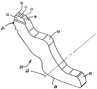
seen in FIG. 3, generally parallel extending ridges 60, 62,
64. While FIG. 3 illustrates three parallel ridges extending
generally parallel to the axis 68, a smaller contact, as shown
in FIGS. 1 and 2, might well be provided with only two ridges
60, 62.
FIG. 1 illustrates the locations of ridges 60, 62
relative to each other at the time of first engagement by lead
58 of device 18. It will be noted that ridge 60 is engaged by
lead 58, and ridge 62 is not. The spacing between lead 58 and
ridge 62, when the contact 24 is in this orientation, is
illustrated by reference numeral 66.
As pressure continues to be applied to device 18, contact
24 will be caused to rotate generally counterclockwise about
axis 68. At some point, lead 58 will engage ridge 62, and
ridge 60 will be rotated downwardly away from lead 58. In the
9
CA 02579697 2007-02-26
case of a three-ridge embodiment, second ridge 62 will also be
withdrawn from lead 58 as third ridge 64 engages the lead.
It has been found that such a multiple contact point
contact 24 is particularly effective in dealing with matte tin
typically provided on lead 58 to facilitate soldering to an
ultimate host board. The multiple ridge construction serves to
help control a buildup of tin on front end 26 of contact 24.
The first ridge 60 has a tendency to collect the most tin. A
non-desirable buildup is deterred by providing multiple
ridges. The first ridge serves a sacrificial function in
absorbing the greatest transfer of tin.
FIG. 3 illustrates a contact 24 having a narrowed front
end 26. Such an embodiment defines a smaller land 71 with
spaced shoulders 72 on either side thereof. Such a feature, it
is envisioned, would be used when the device being tested were
leadless and had a pad generally flush with the bottom of the
body of the device 18. Such a land embodiment could even serve
to function in an environment wherein the pad or pads of the
DUT are recessed within the body of the integrated circuit.
It will be understood that this disclosure, in many
respects, is only illustrative. Changes may be made in
details, particularly in matters of shape, size, material, and
arrangement of parts without exceeding the scope of the
invention. Accordingly, the scope of the invention is as
defined in the language of the appended claims.