Note: Descriptions are shown in the official language in which they were submitted.
CA 02580041 2010-12-31
52701-10
IMPROVED THREE STAGE POWER SOURCE
FOR ELECTRIC ARC WELDING
FIELD OF THE INVENTION
The invention relates to the field of electric arc welding and more
particularly to an
improved three stage power source for such welding and a novel relationship
between the first
two stages of the three stage power source.
BACKGROUND OF INVENTION
Electric arc welding involves the passing of an AC or DC current between a
metal
electrode and a workpiece where the metal electrode is normally a cored metal
wire or solid
metal wire. A power source is used to create a given current pattern and/or
polarity between the
advancing electrode wire and worlcpiece so that the arc will melt the end of
the advancing
welding wire and deposit the molten metal on the worlcpiece. Although various
converter
technologies are used for power sources, the most effective is an inverter
based power source
where a switching network includes switches operated at high frequency to
create the desired
waveform or current level for the welding process. An inverter type power
source is discussed in
Blankenship 5,278,390 where the inverter is controlled by "waveform control
technology"
- 1 -
'
CA 02580041 2010-12-31
52701-10
pioneered by The Lincoln Electric Company of Cleveland, Ohio. The actual
waveform is
generated by a series of short pulses created at a frequency generally above
18 kHz and the group
of short pulses has a profile controlled by a waveform generator. In
accordance with standard
power source technology, the input signal to the inverter stage of the power
source is rectified
current from a sine wave power supply. An appropriate power factor correcting
converter is
common practice and is either a part of the inverter switching network itself,
as shown in Kooken
5,991,169, or is located before the inverter stage, as shown in Church
6,177,645. Indeed, a
power source with a power factor correcting converter or stage has been known
in the welding art
for many years. Another power source employing an input power factor
correcting converter in
the form of a boost converter is shown in Church 6,504,132. In both
Kooken 5,991,169 and Church 6,504,132 the actual welding current is regulated
by an output
chopper or buck converter and isolation is obtained by a transformer either in
the output of the
inverter stage or in the output of the input boost converter. These various
topologies for power
sources are common knowledge in arc welding technology. In these prior art
patents, the actual
welding current, voltage or power is regulated in or before the output stage
of the power source,
which output stage is either an inverter or a chopper. Neither the inverter,
nor the chopper is
unregulated to produce a fixed, lower voltage DC bus for driving a regulated
welding stage.
Isolation of the welding operation is a characteristic of most power supplies
for welding.
The term "welding" includes "plasma cutting." In Vogel 5,991,180, a
preregulator using a boost
converter is directed to a converter which is disclosed as a chopper having an
output isolation
transformer located after welding regulation and directly driving the welding
operation. In this
- 2 -
CA 02580041 2010-12-31
52701-10
power source, the chopper network is controlled to create the desired
regulated output welding
current and isolation is provided in the output stage. In a like manner,
Thomrnes 5,601,741
discloses a boost converter for driving a pulse width modulated controlled
inverter providing the
regulated output signal to the actual welding operation. In both Vogel and
Thonunes, the second
stage-is regulated to direct the power factor controlled current from a
preregulator into a welding
operation. Welding regulation is in the second stage and is normally driven by
a pulse width
modulator control circuit. In Moriguchi 6,278,080 an inverter type power
source is regulated to
control the desired welding current. Isolation is obtained by a transformer
between the controlled
second stage inverter and the welding output which is disclosed as a DC
welding operation. A
similar power source is shown in Moriguchi 5,926,381 and Moriguchi 6,069,811
wherein the
isolation of the control current from the inverter stage is at the output of
the inverter and directly
drives the welding operation. Moriguchi 5,926,381 discloses the common
arrangement for using
the voltage at the output of the first stage boost converter to provide the
controller voltage for
either the regulated inverter stage or the boost converter itself. The three
Moriguchi patents
show the prior art power source
where a regulated inverter is driven by an input boost converter or a DC
output of a rectifier to
produce a controlled welding current directed to an output transformer used
for isolation. The
= secondary AC signal of the isolation transformer is directly used for the
welding operation.
There is no third stage topology as used in the novel power source of the
invention.
Turning now to non-welding technology, an aspect of the invention is the use
of a
synchronous rectifier device at the output of a DC/DC second stage converter.
Synchronous
- 3 -
CA 02580041 2010-12-31
52701-10
=
rectifiers are common practice and one such rectifier is illustrated in Boylan
6,618,274. Calkin
3,737,755, discloses a DC/DC converter for low power use where a fixed
regulated current is
directed to a non-regulated inverter to provide a non variable output DC
signal. Any control of
the non-regulated inverter is at the input side of the inverter so that the
input DC signal is the
only parameter that can be regulated to control the fixed output DC signal of
the inverter. This is
a topography that requires a control of the signal to the inverter so that the
inverter provides a
controlled fixed output signal. The non-welding general background technology
in Boylan and
Calkin shows a synchronous rectifier and a version of a non-
regulated inverter where any regulation is performed before the inverter by
controlling the level
of the input DC signal. Neither of these patents relate to a power source for
welding and are
illustrative of general technical concepts, such as synchronous rectifier
devices
and unregulated inverters. A non-welding two stage AC to DC converter is shown
in Smolenski
5,019,952 for imparting minimum harmonic distortion to the current flowing
into the converter.
The load is not variable and does not require regulation as demanded in a
welding operation.
This patent shows general technology not related in any way to the
demands of a power source for electric arc welding.
These patents constitute the background information relating to a power source
that must
be regulated by a welding operation where such regulation is by a feedback
loop of average
current, average voltage, and power of the actual welding operation. Fixed
load power sources
are not relevant to the invention, except as general technical information.
In the past, an inverter in a power source outputted a welding current
regulated by a
parameter in the welding operation, such as current, voltage or power. This
inverter was
- 4 -
CA 02580041 2010-12-31
52701-10
normally controlled by a pulse width modulator wherein the duty cycle of the
switches operated
at high frequency was controlled by the feedback from the welding operation so
that the duty
cycle was adjusted in a range substantially less than 100%. This type of PWM
controlled
inverter is referred to as a regulated single stage inverter. Such inverter
formed the output of the
power source and was the last stage of the power source. Lower duty cycles
resulted in higher
primary currents and more losses. The efficiency of the inverter varied
according to the duty
cycle adjustment caused by the requirement of regulating the output of the
single stage inverter to
create an output signal suitable for welding. Using a power source where the
final stage is a
regulated single stage inverter resulted in heat losses, lower efficiency,
high cost and increased
component size. For these reasons, some welding source manufacturers have
marketed power
sources as being better than an inverter power source because they do not use
inverters with the
resulting high cost and other difficulties. An inverter stage which had the
dual function of
isolating the output and regulating the current for the purposes of creating a
current suitable for
welding was to be avoided. See Hoverson 6,723,957.
THE THREE STAGE POWER SOURCE
IMPROVED BY THE PRESENT INVENTION
Embodiments of the present invention are used with a three stage power source
for
electric arc welding and plasma cutting wherein the inverter of the power
source is a
second stage as in the past, but is unregulated so that a third stage can be
added to provide
the actual regulation for creating a current suitable for welding. By using
this novel three
stage concept, a number of advantages can be achieved over the prior art.
-.5-
CA 02580041 2010-12-31
52701-10
First, the inverter can operate at a very high frequency of switching whereas
the output
third stage can be a chopper operated at a lower frequency of switching.
Consequently, the
switching frequency is optimized for each stage of the invention. This reduces
the size of the
inverter without increasing the losses of the other stages.
Second, because of the use of the described three stages only one isolation
transformer is
needed for the system. In the prior art, two isolation transformers were
required; one for the
power conversion and one for the control power. However, in the present
invention, because the
second stage outputs an isolated, fixed DC voltage onto a second DC bus
another isolation
transformer is not required to generate the control power. This allows the
complexity, cost and
size of the device to be reduced, while achieving the same or better
efficiency and power.
A third advantage is the higher peak to average power ratios provided by the
present
invention. In prior art systems, the second stage inverter had to be designed
to experience the
full peak power, for which the machine was rated. Accordingly, all components
within the
secOnd stage inverter, including the transformers, had to be designed and
built for this peak
power rating. Such a requirement resulted in very large and complex inverter
designs, because
many components, such as the transfoliners, had to be made very large to
accommodate the peak
powers the machine was rated for. This design requirement is eliminated by
embodiments of
the present invention. As discussed previously, the second stage unregulated
inverter
includes the isolation transformer for the power system, and no other
transformer exists
downstream of this second stage. Because of this, and because of the placement
of a
de-coupling capacitor between the second and third stages, no components of
embodiments of the present invention which are upstream of the de-coupling
capacitor
experience the "peak" power of the system. Stated differently, only the third
- 6 -
CA 02580041 2010-12-31
52701-10
stage will experience the system peak power. Therefore, the second stage
(inverter) of the present invention need only be designed for "average" power,
which greatly reduces the overall size and complexity of the system. The
design
and sizing changes needed to allow the third stage (i.e. a chopper) to handle
system peak power are much simpler and easier to do than designing an
inverter/transformer stage for the same peak power. Accordingly, embodiments
of
the present invention allow for the overall reduction in size for the
inverter/transformer stage, thus achieving the same peak to average power
rating
as prior art devices with a smaller size.
Related to the above advantage is the ability of embodiments of the
present invention to achieve even higher peak to average power ratings than
prior
art devices. Because it is easier and less complex to design and build a third
stage (i.e. chopper) to handle high peak power, the configuration of
embodiments
of the present invention allows for the overall system to have a higher peak
to
average power rating than prior art devices. This is achieved while still
maintaining a relatively small size. In an embodiment of the invention the
peak
power is 4 x average power, and in another embodiment can be as high as
5 x average power. Such an improvement is highly advantageous in pulse
welding, where the peak to average power rating of a machine can be important.
An additional advantage is the high operating efficiency that can be
obtained for the first and second stages of embodiments of the present
invention.
In prior art devices, the operational efficiency of the power factor
correction (PFC)
and isolation stages is relatively low, and can be as low as 82%, but is
typically 86%. However, embodiments of the present invention can obtain
operational efficiency as high as 90%, and higher. As further discussed below,
an
embodiment of the present invention contains PFC in the first stage and
provides
an isolated inverter stage in the second stage. Because the second stage is
unregulated, and is operating at a very high duty cycle (discussed below) the
- 7 -
CA 02580041 2010-12-31
52701-10
overall system efficiency between the PFC and inverter/isolation stages can be
as high as 90%, or
even higher.
A further advantage, is that an embodiment of the present invention does not
require
phase shifting in the unregulated inverter stage (second stage). In prior art
systems using high
power (such as welding and cutting systems) "soft switching" (discussed in
more detail below),
in an inverter stage, required phase shifting. Namely, because the inverter
stage's "ON" time is
not fixed, it is necessary for prior art systems to use phase shifting
techniques to achieve soft
switching. By having a non-fixed duty cycle the efficiency of the prior art
systems was limited.
Further, the use of phase shifting adds complexity and contributes to power
loss in the inverter.
Embodiments of the present invention obviate the need for phase shifting due
to the novel aspects of the system
construction and design. Specifically, in an embodiment of the present
invention, the inverter
stage is unregulated and is operating at a high and fixed duty cycle of at
least 80%, and in another
embodiment at least 90%, and in a further embodiment near 100%. Because of
these high fixed
duty cycles, this embodiinent of the present invention does not require phase
shifting.
Essentially, the second unregulated stage of the present invention has
inherent soft switching. By
having a high, fixed duty cycle energy that is stored in the leakage
inductance of the transformer
is used to force zero voltage across IGBT's before they are turned on. This
results in soft
switching of the switches. This is an advantage when compared to regulated
inverters of the
prior art, because regulated inverters require some type of phase shift
modulation in order to have
soft switching. This is typically because the duty cycle in a regulated
inverter varies and there is
not a known, fixed "off' time. Further, often in prior art systems, in
addition to phase shift
control, it is also common to add a certain amount of leakage inductance or
alternative circuits in
- 8 -
CA 02580041 2010-12-31
52701-10
order to make sure the lagging leg is soft switched. The complexities
associated
with soft switching a regulated inverter are eliminated by this embodiment of
the
present invention, which employs an unregulated inverter operating at a high,
fixed duty cycle, allowing inherent soft switching without the need for phase
shifting.
It is noted that the overall aspect of the three stage topography, of
embodiments of the present invention, is not limited to using only an inverter
stage
which does not use phase shifting. It is understood that certain advantages of
embodiments of the present invention may be obtained by using an inverter
stage
which does employ phase shifting to assist/enable soft switching.
Furthermore, the isolated, fixed DC voltage to the regulated third
stage can be substantially lower than the DC voltage from the input converter
stage and much higher than the actual welding output voltage.
The three stage power source using embodiments of the invention
involves a novel topography for a power source wherein the pulse width
modulated inverter is merely a second stage for creating an isolated fixed
output
DC bus without a feedback signal to the second stage pulse width modulated
inverter. This isolated bus is used in a third stage regulated by the actual
welding
parameters to create a current suitable for welding. Consequently, embodiments
of the invention involve an unregulated second stage not only providing
necessary
isolation but also producing a fixed DC output bus to be used by a third stage
wherein welding regulation is accomplished. The unregulated second stage
inverter is operated at a very high frequency with a duty cycle that is fixed
during
operation of the power source. In an embodiment of the present invention, the
frequency is over 18 kHz and in another embodiment can be about 100 kHz. As
stated above, the duty cycle is fixed at various high levels. In one
embodiment,
the duty cycle is fixed at least
- 9 -
CA 02580041 2007-03-01
80%, whereas in another embodiment the duty cycle is fixed at least 90%, and
in an additional
embodiment the duty cycle is close to 100% to give the maximum efficiency
level. The use of a
fixed, high duty cycle minimizes the current circulation time of the inverter
second stage to
substantially reduce heat and increase efficiency. The inverter second stage
may be phase shift
modulator controlled, or may not employ phase shifting at all, as described
above.
The output of the second unregulated inverter stage can be a rectifier using
well known
synchronous rectifier devices, which devices are,controlled by the secondary
winding of the
internal isolation transformer of the second stage unregulated inverter. By
using synchronous
rectifier devices at the output of the second stage, there is further
improvement in the total
efficiency of the power source. The first stage is either an input rectifier
or an input rectifier with
a power factor correcting converter. In an exemplary embodiment, a first stage
power factor
correcting converter is employed. This converter is after a standard rectifier
or can be combined
with the rectifier. Of course, this converter can be a passive power factor
correcting converter or
an active converter such as a boost, buck or buck+boost converter. The first
stage of the
invention produces a first DC bus with a fixed voltage. As stated previously,
the overall
efficiency of the first PFC stage and unregulated inverter stage (isolation
stage) of the present
invention can be as high as 90% and higher.
By using a standard first stage for the power source, the first DC output
signal which is
the input DC bus to the unregulated inverter can be regulated and fixed at a
value of about 400-
900 volts DC, in an exemplary embodiment. The output of the unregulated,
isolation inverter
forming the second stage of the novel power source is a fixed DC bus having a
fixed relationship
with the input DC bus from the first stage The voltage of the second DC bus or
output is
-10-
CA 02580041 2010-12-31
52701-10
substantially less than the voltage of the DC bus from the first stage. For
example, in an
embodiment of the invention the first DC bus may have a voltage of 400V where
the second DC
bus has a voltage of 100V.
The power source thus produces a second DC bus which has a fixed mathematical
relationship with the input DC bus from the power factor correcting converter.
In accordance
with standard practice, the second stage unregulated inverter includes an
isolation transfoimer
having a primary winding and a secondary winding so that the secondary winding
is isolated
from the input of the power source. See Steigerwald 4,864,479. The
unregulated, second stage inverter can be operated at a switching frequency to
optimize the
operation of the second stage inverter. In an embodiment of the invention,
extremely high
switching frequency is used to reduce the size and cost of the components in
the novel,
unregulated second stage inverter. Indeed, in an exemplary embodiment, the
duty cycle is fixed
at least 80%, and in a further embodiment at least 90% and in an additional
embodiment at close
to 100%. This drastically reduces the circulated current in the second stage
and greatly improves
the operating characteristics of the second stage inverter which also provides
the function of
isolating the welding output of the power source from the AC input of the
power source. By
having the switching devices in the second stage unregulated inverter operated
at full on, this
inverter has a high efficiency and is very flexible in operation.
An isolation transformer determines the relationship between the fixed DC bus
at the
input side of the unregulated second-stage (a "first DC output signal" from
the first stage) and the
DC output bus at the output of this second stage (a "second DC output
signal"). In some prior art
power sources, the duty cycle at the primary winding of the isolation
transformer in the regulated
-11-
CA 02580041 2010-12-31
52701-10
inverter is regulated by the welding operation. There is no regulation by the
welding operation in
either the first stage or second stage of the novel three stage power source
to which
embodiments of the present invention are directed.
A power source for electric arc welding having an active power factor
correcting feature
and tight output control of the energy directed to the welding operation
requires at least two
switching stages. These two stages assure that instantaneous energy
transferred into the power
source and transferred out the power source can be regulated independently
with appropriate
energy storage components. Thus, a power factor correcting power source for
electric arc
welding generally requires two independent switching control circuits. One of
the control
circuits is used to control the energy or the output current for the welding
operation. The other
control circuit is used to control the DC signal from the active power factor
correcting converter
forming the first stage of the power source. Thus, electric arc welding power
sources having
power factor correcting capabilities requires two switching networks each of
which has
independent control requirements. The first switching control is for the
output welding current
and the other switching control is for power factor correcting at the input
stage of the power
source. This second switching control assures that the output of the first
stage is a fixed DC
voltage referred to as a "DC bus." The voltage of the DC bus itself is used to
control the first
stage converter to assure that the DC bus from this converter has a fixed
voltage level. To
recapitulate an inverter based power source for electric arc welding requires
two separate
switching networks and two control circuits for these networks.
An inverter based power source for electric arc welding has another conceptual
requirement. One of the stages in the power source must provide electrical
isolation between the
- 12 -
CA 02580041 2007-03-01
variable input AC signal and the regulated output current suitable for
welding. The isolation
device is normally in the form of a transformer. In prior art, two stage
inverter based power
sources there are two locations for the isolation device. In the first
example, the power factor
correcting input stage is not isolated and an isolation transformer is
provided in the second stage
regulated output inverter. In another example, isolation is in the first stage
power factor
correcting converter. In this second example, a non-isolation output inverter
or other non-
isolation converter can be used as the second stage. The first example is more
efficient than the
second example due to 60 Hz effect on the RMS current at the input side of the
power source. In
recapitulation, the second conceptual requirement of a welding power source is
isolation.
The two requirements of an active power factor correcting power source for
welding are
(a) two separate and independent control circuits for two separate switching
networks and (b) an
appropriate structure for isolating the input of the power source from the
output of the power
source. These basic requirements of inverter based power sources are
implemented in an
embodiment of the three stage power source. As previously discussed, in an
embodiment of the
present invention, the unregulated second stage is an isolation stage between
two regulated non-
isolation stages to form a unique arrangement involving a three stage inverter
based power
source. The novel three stage power source is more efficient than the two
stage inverter based
power source assuming the same power factor correcting preregulator is used.
Thus, the novel
three stage power source is more efficient, but still has the essential
characteristics required for a
power source used in electric arc welding. There are two independently
controlled switching
networks. There is an isolation stage. These constraints are accomplished in a
manner to
-13-
CA 02580041 2010-12-31
52701-10
increase efficiency and obtain better welding performance and better heat
distribution of the
power switching components.
Since the second unregulated inverter stage of the three stage power source
provides
system isolation, many types of non-isolated converters can be used as the
power factor
correcting preregulator, thus adding to the simplicity and versatility of
embodiments of the present
invention. A boost converter is the most popular converter due to the current
shaping function and the
continuous line current characteristics of this type of conversion. However,
the output voltage of
the boost converter is higher than the peak of the highest line voltage, which
peak can be as high
as 775 volts, for example. Thus, other active power factor correcting
regulators can be used with
the invention, which is a three stage power source wherein the second stage is
unregulated and
provides isolation. One of the other options for the active power factor
correcting input or first
stage is a step-up/step-down converter so that the primary voltage bus or
input bus to the second
stage can be lower than the peak of the input AC voltage signal to the power
source. This type of
power factor correcting converter still produces low harmonics. One such power
factor converter
is referred to as a buck+boost converter.
Thus, in an exemplary embodiment, a 400 volt to 500 volt DC bus used for the
second
stage is obtained with an input AC voltage in the range of 115 volts to 575
volts. In this
embodiment, irrespective of the AC voltage to the first stage, the output
voltage of the active
power factor converter is controlled to be at a level between 400 volts and
500 volts. Other types
of active and passive power factor correcting inverters can be used in the
invention, In an
exemplary embodiment, the converter is active thus constituting a second
switching network
requiring a second control circuit.
- 14 -
CA 02580041 2007-05-10
=
When using the term electric arc welding, it also includes other output
processes, such as
plasma cutting.
As so far explained, the three stage power source using the invention involves
a three
stage power source for electric arc welding. A feedback control in the third
stage creates an
output current suitable for welding. The input first stage is normally an
active power factor
correcting converter requiring a second switching network and a second
independent control
circuit. This three stage topography is not used or disclosed in the prior
art. By having this
topography, the added second stage is used to convert the high voltage DC bus
at the primary
side of the second stage to a lower voltage DC bus at the secondary side of
the second stage
isolated from the primary side. Thus, the three stage involves a DC bus at the
secondary side of
the second stage so that the bus can be used for regulation of welding power.
The term "bus"
means a DC signal that has a controlled fixed level. The three stage power
source has a first DC
bus from the input stage called the "first DC output" which first DC output
has a controlled DC
voltage. There is a second DC bus at the secondary side of the second stage
called the "second
DC output" which second DC output is also a controlled DC voltage level. The
creation of a
second DC bus at the secondary side of an unregulated inverter has advantages,
other than the
advantages associated with the use of the unregulated second stage inverter as
so far described.
The secondary DC bus or second DC output is isolated from the primary side of
the second stage
so that there is no isolation required in the third stage welding control
circuit. In other words, the
output control circuit, such as a chopper, has an input DC bus with a fixed
voltage level, In
practice, the chopper has a controller with a control voltage that is derived
from the input DC to
the chopper. This input DC signal is isolated from the input power.
Consequently, the control
-15-
CA 02580041 2010-12-31
52701-10
voltage for the controller of the output stage or chopper can be derived from
a non-isolated DC
source. This is normally the input signal to the chopper. Separate isolation
of the control voltage
for the controller used in the output stage is not required. The use of a
fixed DC bus from the
second stage allows the DC voltage to the output third stage, which is
regulated by the welding
operation, to be much lower than the normal input primary DC bus ("first DC
output") of the
power source. In the past, the output of the power factor converter is a
relatively high level DC
signal based upon the use of a boost converter. This high DC voltage was
directed to the
regulated inverter stage for use in outputting a current suitable for the
welding. By using
embodiments of the present invention the high voltage from the output bus of
the power factor
converter is drastically reduced. It is more efficient to convert a 100volt DC
bus into a 15 volt
control power than to convert a 400 volt DC bus to a 15 volt control power.
Additionally, this aspect of the present invention allows for the easy supply
of external
power for external devices such as lights, additional power tools, etc. In
prior art devices,
because the DC bus has such a high voltage, it is necessary to step down and
isolate the bus from
any external devices that may draw their power from the power supply. Such
stepping down and
isolation required additional components, complexity and cost. With
embodiments of the present
invention, this is avoided, as the second DC bus, is already isolated and the
voltage (which can be 100V)
is such that no additional or significant components are needed between the DC
bus and any external
device. Again, the present invention provides significant size, cost and
complexity advantages
over the prior art.
A second stage of the three stage power source is in the form of an
unregulated DC to DC
converter has an input connected to the first DC output signal and an output
in the form of a
- 16-
CA 02580041 2010-12-31
- 52701-10
second DC output signal electrically isolated from the first DC output signal
with a magnitude of
a given ratio to the first DC output signal. The power source includes a third
stage to convert the
second DC output signal to a welding current for the welding process. The
third stage of the
power source includes a regulated converter such as a chopper or inverter.
When using an
inverter, the output is a DC signal directed to a polarity network or switch,
which switch allows
DC welding by the power source. The polarity switch allows welding either DC
negative, DC
positive or AC. The welding process, using either a chopper or an inverter,
can be performed
with shielding gas, such as MIG welding, and can use any type of electrode,
such as tungsten,
cored wire or solid metal wire. In accordance with an aspect of the invention,
the output of the
unregulated DC to DC converter is substantially less than the input to the
second stage. In most
instances, the input and output of the second stage are DC voltages with
generally fixed
magnitudes.
SUMMARY
There are several benefits to operating welding inverters with high switching
speeds. For
instance, smaller magnetics translate into improved portability. Another
advantage is the
potential to have a higher band width control system, which system will result
in a better arc
performance. An embodiment of the three stage power source, of the present
invention, has
power switches operated at extremely high switching speed, exceeding 18 kHz,
and in a further
embodiment can be higher, such as 100 k_Hz. The boost power switch for the
first stage and the
four power switches for the unregulated second stage are all operated at high
frequency to obtain
the benefit of high switching speed. In the prior art, there is a downside to
the use of such higher
switching speeds. Such switching speeds cause switching losses. If the
switching losses are not
- 17 -
CA 02580041 2010-12-31
52701-10
reduced the power source efficiency and reliability are decreased. The
switching losses are
caused by the overlap of current and voltage during switching, either from the
on condition to the
off condition or from the off condition to the on condition. To reduce the
switching losses, either
the voltage or the current must be held near zero during the switching.
Switching transition can
be either zero voltage or zero current or both. This is called "soft
switching." What are termed
resonant or quasi resonant techniques have heretofore been used to obtain soft
switching by zero
voltage or zero current at high switching speeds. However, this type of prior
soft switching
control often causes higher current and voltage stresses because of the
sinusoidal waveforms and
still has conduction losses. However, there are prior soft switching circuits
that employ zero
voltage transition converters or zero current transition converters in a
manner to reduce both the
switching losses and the conduction losses.
In one embodiment of the present invention, the unregulated second stage
inverter of the
novel three stage power source uses a phase shift PWM
to control the output power. By fixing the phase shift at a high level near
100%, and in another
embodiment above 80%, the switching losses in the second unregulated stage are
limited. By
using a fixed phase shift PWM control the second stage is operated near full
conduction to
produce low conduction losses.
In a further alternative embodiment, as discussed previously, the second
unregulated
inverter stage does not employ any phase shifting as it is not needed. This
embodiment provides
even higher system efficiency then the phase shifted embodiment and is simpler
and more
efficient in its construction, as discussed previously.
- 18 -
CA 02580041 2010-12-31
52701-10
Specifically, in this embodiment of the present invention, the inverter stage
is unregulated
and is operating at a high and fixed duty cycle of at least 80%, and in
another embodiment at
least 90%, and in a further embodiment near 100%. Because of these high fixed
duty cycles, this
embodiment of the present invention does not require phase shifting. By having
a high, fixed
duty cycle energy that is stored in the leakage inductance of the transformer
is used to force zero
voltage across IGBT's before they are turned on. This results in soft
switching of the switches.
This is an advantage when compared to regulated inverters of the prior art,
because regulated
inverters require some type of phase shift modulation in order to have soft
switching. This is
typically because the duty cycle in a regulated inverter varies and there is
not a known, fixed
"off' time. Further, often in prior art systems, in addition to phase shift
control, it is also
common to add a certain amount of leakage inductance or alternative circuits
in order to make
sure the lagging leg is soft switched. The complexities associated with soft
switching a regulated
inverter are eliminated by this embodiment of the present invention, which
employs an
unregulated inverter operating at a high, fixed duty cycle, allowing inherent
soft switching
without the need for phase shifting. Thus, regardless of the embodiment used,
phase shifted or
not phase shifted, the second unregulated stage is soft switched inherently.
In accordance with an alternative embodiment the invention, the three stage
power source
described above has soft switching in the input stage. To this end,
embodiments of the present invention involve the use of an active soft
switching circuit for the
first input stage to be combined with the inherent soft switching of the
second unregulated
stage. This combination of added soft switching with inherent soft switching
has substantially
increased the efficiency of the novel three stage power source.
- 19 -
CA 02580041 2010-12-31
52701-10
The active soft switching circuit of the first stage is the type circuit
described in a 1991 article by the IEEE entitled High Efficiency Telecom
Rectifier
using A Novel Soft-Switching Boost-based Input Current Shaper. This type
circuit
is also described in a 2002 article entitled A New ZVT-PWM DC-DC Converter by
the IEEE. This article from the IEEE Transaction on Power Electronics is dated
January 2002. Another active circuit for soft switching is a voltage
transition-current transition circuit described in a 2004 article entitled A
New
ZVT-ZCT-PWM DC-DC Converter published by IEEE Transactions on Power
Electronics published in May, 2004. These articles describe an active soft
switching circuit or circuits of the type used in the first stage of a three
stage
power source. Embodiments of the invention combine an active soft switching
for
the first input stage and an inherently soft switched unregulated inverter
using
either a phase shift PWM control or without any phase shift, as described
above.
SteigenNald 4,864,479 shows a common unregulated inverter using phase shift
control. This type of unregulated power stage has a topography that increases
the
efficiency by minimizing the circulating currents through the use of a fixed
high
duty cycle switching operation. The unregulated inverter operated at a fixed
duty
cycle will achieve soft switching on all the primary switches with a minimum
amount of conduction losses. This concept is used in one embodiment of the
second stage of the three stage power source to which the invention is
directed.
In accordance with embodiments of the invention, the high switching
speed power switch of the first stage of a three stage power source is soft
switched with an active circuit to reduce both the losses of the switch and
the
losses of the output rectifier. Furthermore, the soft switches input stage is
- 20 -
CA 02580041 2007-05-10
combined with a second stage having an inherent soft switching capability
using a fixed duty
cycle, and either a phase shift unregulated inverter or an unregulated
inverter without phase shift.
The combination of an active soft switching circuit for the first stage
combined with the inherent
soft switching of a fixed duty cycle unregulated inverter substantially
increases the efficiency of a
three stage power source of the novel type to which the present invention is
directed. With this
aspect of the invention, an embodiment of the invention can achieve high
efficiency and a fixed
duty cycle of at least 80%, and can be as high as at least 90%, and in further
embodiments can
approach 100%.
By using an active soft switching circuit on the first input stage of the
three stage power
source, the pulse width modulator converter of the first stage has zero
voltage switching for the
active converter switch and zero reverse recovery current for the output
diode. This soft
switching is without increasing voltage or current stresses, i.e. conduction
losses of the two
components. This soft switching circuit for the power switch (active) for the
first stage includes
a zero voltage transition using a network with an inductance branch and
capacitor branch both in
parallel with both the active pulse width modulating power boost switch and
the passive output
switch or output boost diode. The two branch network includes an induction
branch capacitance
branch controlled by switching of an auxiliary switch. The auxiliary switch is
also connected in
parallel with the pulse width modulated power boost switch and is turned on
for a short interval
just prior to the turn on of the pulse width modulated switch. The network
inductor current
ramps up until it turns off the output rectified diode, communicating it with
a soft switching
operation. The inductor current continues to increase bringing the voltage
across the pulse width
modulated circuit to zero at a time prior to the turn on of the boost switch.
An anti-parallel diode
-21-
CA 02580041 2010-12-31
52701-10
of the pulse width modulator switch is thus forward biased. The turn on signal
for the power
switch is applied while the anti-parallel diode is conducting to provide a
zero voltage switching
of the modulating switch at turn on. The auxiliary switch is then turned off
and the modulating
power switch is turned on. The auxiliary diode and capacitor provides a
snubber to the voltage
across the auxiliary switch so that the auxiliary switch is not stressed at
turn off. The inductor
branch current rapidly drops to zero, at which time the auxiliary switch turns
off. The remainder
of the operation is the same as that of a conventional pulse width modulated
boost converter,
except the energy stored in the two branch network is transferred to the load
when the main
switch is turned off. In some descriptions of these two branches, they are
referred to as a
resonant circuit which may be technically true, but not necessary to the soft
switching function.
The auxiliary switch controlled two branch circuit is used in the first stage
of
embodiments of the present invention to provide soft switching of both the
power switch and the
output diode. Such a circuit is described in Hua 5,418,704. Soft switching of
the first stage and the
natural soft switching of the second stage is the result of using embodiments
of the present invention.
In accordance with embodiments of the present invention, there is provided a
three phase power
source for an electric arc welding process. This power source comprises an
input stage having an AC
input and a first DC output signal, a second stage in the form of an
unregulated DC to DC converter
having an input connected to the first DC output signal, a network of switches
switched at a high
frequency with a given duty cycle to convert the input signal into a first
internal AC signal, and
an isolation transfoliner with a primary winding driven by the first internal
high frequency AC
signal and a secondary winding for creating a second internal high frequency
AC signal and a
rectifier to convert the second internal AC signal into a DC output signal of
the second stage.
- 22 -
CA 02580041 2010-12-31
52701-10
The magnitude of the output signal for one embodiment of the second stage is
related to the fixed
amount of overlap between the phase shifted switches, which use phase shift
controlled by a
pulse width modulator so that the second stage is inherently soft switched.
With no phase
shifting, in an alternative embodiment, the magnitude of the output is related
to the fixed amount
of ON time.
In an embodiment of the invention, the third stage in the power source is used
to convert
the second DC output signal from the second stage to a welding output for the
welding process.
This three stage power source is improved by providing a DC to DC converter in
the first stage,
where the converter has a power switch with a soft switching circuit. Thus, a
soft switching
circuit to the first stage compliments the inherent soft switching of the
unregulated second stage
to increase the efficiency of the first two stages in the three stage power
source.
In accordance with another aspect of the present invention, the soft switching
circuit of
the first input stage of the three stage power source is an active snubber
circuit with an auxiliary
switch operated in unison with the power switch to positively drive the
voltage toward zero
during both switching transitions. The DC to DC converter of the first stage
has an output or
boost diode which is also soft switched by the first stage soft switching
circuit. In accordance
with another aspect of the invention, the DC to DC converter of the first
stage has a positive and
a negative output lead with a capacitor joining the leads and a diode clamping
the positive end of
the auxiliary switch to the positive output lead. hi an embodiment of the
invention, the three
stage power source with the unique combination of an active soft switching on
the first stage and
an inherent soft switching on the second stage is used with a third stage
chopper. In an option,
the output chopper has a soft switching circuit for its power switch.
All of these features of embodiments of the
- 23 -
-
CA 02580041 2013-04-23
79769-22
present invention improve a three stage power source having as is novel
feature a center
unregulated, isolation stage to increase the efficiency of the power source
while maintaining
the advantage of its three stage topography.
Some embodiments of the present invention relate to the combination of an
input stage and an unregulated center stage of a three stage power source,
wherein the first
stage has an active soft switching circuit for the boost power switch and an
inherent soft
switching for the unregulated second stage. Consequently, embodiments of the
invention
involve a two stage AC to DC converter comprising an input stage having an AC
input and a
first DC output signal and a second stage. The second stage is in the form of
an unregulated
DC to DC converter having an input connected to the first DC output signal, a
network of
switches switched at a high frequency with a given duty cycle to convert the
input into a first
internal AC signal, an isolation transformer with a primary winding driven by
the first internal
high frequency AC signal and a second winding for creating a second internal
AC signal and a
rectifier to convert the second internal AC signal into a second DC output
signal of the second
stage. In the embodiment of the invention using phase shift in the unregulated
inverter, the
magnitude of the output signal for the second stage is related to the amount
of overlap
between the phase shifted switches. In an embodiment without phase shift in
the unregulated
inverter stage the magnitude of the output signal is related to the fixed "ON"
time value. The
input stage includes a power switch having a soft switching network which
network is an
active snubber circuit with an auxiliary switch operated in unison with the
power switch of the
first stage.
According to another aspect of the invention, there is provided a power source
for welding; comprising: a first stage to receive a first signal and output a
second signal
having a first DC voltage; a second stage to receive said second signal and
output an isolated
third signal having a second DC voltage; and a third stage to receive said
third signal and
output a welding signal; wherein said second state comprises an unregulated
inverter stage
having a duty cycle of at least 80% and does not require a phase shift
modulation.
24
CA 02580041 2010-12-31
52701-10
A further aspect of the invention provides a power source for
welding; comprising: a first stage to receive a first signal and output a
second
signal having a first DC voltage; a second stage to receive said second signal
and
output an isolated third signal having a second DC voltage, said second stage
having a single transformer; and a third stage to receive said third signal
and
output a welding signal; wherein at least one of said first and third stages
is
regulated, said single transformer is the only transformer within said power
source, and said second stage is unregulated having a soft switching circuit
which
does not use phase shifting for soft switching.
There is also provided a power source for welding; comprising: a
first stage to receive a first signal and output a second signal having a
first DC
voltage; a second stage to receive said second signal and output an isolated
third
signal having a second DC voltage; and a third stage to receive said third
signal
and output a welding signal, at least one of said first and third stages being
regulated; wherein said power source produces a peak power and an average
power and has a peak to average power ratio of at least 4, and said second
stage
is unregulated having a soft switching circuit which does not use phase
shifting for
soft switching.
In accordance with a still further aspect of the invention, there is
provided a power source for welding; comprising: a first stage to receive a
first
signal and output a second signal having a first DC voltage; a second stage to
receive said second signal and output an isolated third signal having a second
DC
voltage, said second stage being unregulated and having a soft switching
circuit;
and a third stage to receive said third signal and output a welding signal, at
least
one of said first and third stages being regulated; wherein said soft
switching
circuit does not use phase shifting for soft switching.
The primary object of some embodiments of the present invention is
the provision of a novel three stage power source wherein the first stage has
an
active soft switching circuit for the fast switching power switch and the
second
stage is an unregulated inverter forming a part of an isolation stage, which
inverter
- 25 -
CA 02580041 2010-12-31
52701-10
has a soft switching characteristic based upon a fixed high duty cycle for its
several switches.
Another object of some embodiments of the present invention is the
provision of a two stage inverter for use in power conversion, which converter
includes a power switch with an active soft switching circuit and the second
stage
involves an unregulated inverter with a fixed duty cycle controlled by phase
shift in
one embodiment, and having no phase shift control in a second embodiment.
Yet another object of some embodiments of the present invention is
the provision of a three stage power source, as defined above, which three
stage
power source also includes an output stage in the form of a chopper with the
power switch of the chopper having a passive soft switching circuit.
Yet a further object of some embodiments of the present invention is
the provision of a three stage power source, as defined above, which power
source includes an active soft switching circuit for the first stage, an
inherent soft
switching characteristic for the second stage, and a passive soft switching
circuit
for the third stage.
These and other objects and advantages will become apparent from
the following description taken together with the accompanying drawings.
BRIEF DESCRIPTION OF DRAWINGS
(THREE STAGE POWER SOURCE)
The advantages, nature and various additional features of the
invention will appear more fully upon consideration of the illustrative
embodiments
of the invention, which are schematically set forth in the figures, in which:
- 25a -
CA 02580041 2007-05-10
FIGURE 1 is a block diagram illustrating a three stage power source and
disclosing an
embodiment of the three stage power source improved by the invention;
FIGURE 2 and FIGURE 3 are block diagrams similar to FIGURE 1 disclosing
further
embodiments of the three stage power source;
FIGURES 4-8 are partial block diagrams illustrating the three stage power
source with
different first stage embodiments;
FIGURE 9 is a block diagram showing the last two stages of the three stage
power source
wherein the output stage provides AC welding current;
FIGURE 9A is a block diagram of a waveform technology control circuit for use
in the
three stage power source illustrated in FIGURE 9, together with graphs showing
three welding
waveforms;
FIGURE 10 is a block diagram illustrating a second and third stage of the
three stage
power source wherein the output stage is DC welding current;
FIGURE 11 is a block diagram illustrating the topography of the three stage
power source
for creating current suitable for electric arc welding with two separate
controller, control voltage
supplies;
FIGURE 12 is a block diagram illustrating a specific three stage power source
employing
the topography to which the present invention is directed;
FIGURES 13-16 are wiring diagrams illustrating four different circuits for
correcting the
power factor in the first stage of the three stage power source;
-26-
CA 02580041 2007-05-10
FIGURE 17 is a combined block diagram and wiring diagram illustrating the
preferred
embodiment of the unregulated inverter constituting the novel second stage of
the three stage
power source to which the present invention is directed;
FIGURES 18-21 are wiring diagrams showing several inverters used as the second
stage
unregulated, isolation inverter comprising the novel aspect of the three stage
power source to
which the present invention is directed;
FIGURE 22 is a wiring diagram of the first input stage and second isolation
stage forming
an embodiment of the present invention;
FIGURE 23 is a wiring diagram of a second embodiment of the present invention;
FIGURE 24 is a wiring diagram illustrating a three stage power source wherein
the output
stage is a chopper with a passive soft switching circuit;
FIGURE 25 is a wiring diagram showing the active soft switching circuit used
in the
embodiment of the invention shown in FIGURE 22;
FIGURE 26 is a wiring diagram showing the active soft switching circuit used
in the
preferred embodiment of the invention; and,
FIGURE 27 is a graph of the voltage curves and trigger signals for the main
power switch
and the auxiliary switch of the circuit illustrated in FIGURE 26.
THREE STAGE POWER SOURCE
(Figures 1-21)
The present invention is a novel three stage power source for use in electric
arc welding.
The new three stage power source has an input stage for converting an AC
signal into a first DC
output bus. This output bus has a fixed voltage level and is directed to the
input of a second
-27 -
CA 02580041 2007-05-10
= =
=
stage, and embodiment of which is shown in FIGURE 16. This novel second stage
of the three
stage power source is an unregulated inverter which includes an isolation
feature and has a
second DC output or second DC bus which is proportional to the DC input bus.
The level
relationship is fixed by the construction of the unregulated inverter. The
unregulated second
stage inverter has a switching network wherein the switches are operated at a
high switching
frequency greater than 18 kHz and in another embodiment can be as high as
about 100 kHz. The
switching frequency of the switch network in the unregulated inverter forming
the second stage
of the power source allows use of small magnetic components. The isolated DC
output of the
unregulated inverter is directed to a third stage of the power source. This
third stage can be
either a chopper or inverter which is regulated by a welding parameter, such
as current, voltage
= or power of the welding operation. In an embodiment of the invention this
third stage is a
chopper. The topography of the three stage power source has an input stage to
produce a first DC
signal, a second unregulated DC to DC stage to provide an isolated fixed DC
voltage or DC bus
that is used by the third stage of the power source for regulating the current
used in the welding
operation. Three examples of a three stage power source to which the present
invention is
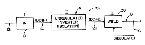
directed are illustrated in FIGURES 1-3. Power source PS1 in FIGURE 1 includes
first stage I,
second stage II, and third stage III. In this embodiment, stage I includes an
AC to DC converter
for converting AC input signal 12 into a first DC bus 14. The input 12 is an
one phase or
three phase AC line supply with voltage that can vary between 200-700 volts,
in an exemplary
embodiment. Converter 10 is illustrated as an unregulated device which can be
in the form of a
rectifier and filter network to produce DC bus 14 identified as (DC#1). Since
the AC input
signal is a line voltage, DC bus 14 is generally uniform in magnitude.
Unregulated inverter A is
-28-
CA 02580041 2007-05-10
=
a DC to DC converter with an isolation transformer to convert the DC bus 14
(DC#1) into a
second DC bus or second DC output 20 (DC#2). Output 20 forms the power input
to stage fa
which is converter 30. The DC voltage on line 20 into a current suitable for
welding at line B. A
feedback control or regulation loop C senses a parameter in the welding
operation and regulates
the current, voltage or power on line B by regulation of converter 30. In
practice, converter 30 is
a chopper, although use of an inverter is an alternative. By having a three
stage power source
PS1 as shown in FIGURE 1, the switching network of the second stage has a
frequency that is
normally higher than the switching frequency of converter 30. Furthermore, the
DC voltage in
line 20 (DC#2) is substantially less than the DC voltage from stage I on line
14 (DC#1).
In an embodiment, there is an isolation transformer in inverter A. The
transformer has an
input or primary section or side with substantially more turns than the
secondary section or side
used to create the voltage on line 20. In an embodiment of the present
invention, the turn ratio in
practice is 4:1 so that the voltage on line 20 is 1/4 the voltage on line 14.
In an example the
voltage on DC #1 is around 400 volts, where the voltage on DC#2 is around 100
volts.
The general topography of three stage power source to which the present
invention is
directed is illustrated in FIGURE 1; however, FIGURE 2 illustrates an
implementation wherein
power source PS2 has essentially the same stage II and stage Ta as power
source PS1; however,
input stage I is an AC to DC converter 40 including a rectifier followed by a
regulated DC to DC
converter. The converted signal is a DC signal in line 14 shown as a first DC
bus (DC#1). The
voltage on line 14 is regulated as indicated by feedback line 42 in accordance
with standard
technology. Thus, in power source PS2 the output welding converter 30 is
regulated by feedback
loop C. The voltage on line 14 is regulated by feedback loop shown as line 42.
Since converter
- 29-
CA 02580041 2007-05-10
=
40 is a power factor correcting converter it senses the voltage waveform as
represented by line
44. By using power source PS2, the first DC bus 14 is a fixed DC voltage with
different one
phase or three phase voltages at input 12. Thus, output 20 is merely a
conversion of the DC
voltage on line 14. DC#2 is a fixed voltage with a level determined by the
isolation transformer
and the fixed duty cycle of the switching network in unregulated inverter A.
This is an
exemplary implementation of the novel power source employing three separate
and distinct
stages with stage If being an unregulated inverter for converting a fixed
first DC output or DC
bus to a second fixed DC output or DC bus used to drive a regulated welding
converter, such as a
chopper or inverter. As another alternative, stage I could be regulated by a
feedback from the DC
#2 bus in line 20. This is represented by the dashed line 46 in FIGURE 2.
Power source PS3 in FIGURE 3 is another implementation of the three stage
power
source. This is an alternative implementation; however, the three stage power
source of the
present invention can have the input converter 50 regulated by feedback loop
52 from the
welding current output B. With this use of a three stage power source,
converter 50 is regulated
by the welding output and not by the voltage on line 14 as in power source
PS2. With regulation
from welding output B, converter 50 is both a power factor correcting stage
and a welding
regulator. However, this implementation of the three stage power source is
disclosed for a
complete technical disclosure.
As previously described, input stage! converts either a single phase or a
three phase AC
signal 12 into a fixed DC bus 14 (DC#1) for use by the unregulated inverter A
constituting
second stage II. The novel three stage power source generally employs a DC to
DC converter in
stage Ito produce the DC voltage indicated as line 14 in FIGURES 1-3. The DC
to DC converter
-30-
CA 02580041 2007-05-10
=
of stage I can be selected to create the desired voltage on line 12. Three of
these converters are
shown in FIGURES 4-6 wherein an input rectifier 60 provides a DC voltage in
lines 60a, 60b to a
DC to DC converter which may be a boost converter 62, a buck converter 64 or a
buck+boost
converter 66, as shown in FIGURE 4, FIGURE 5 and FIGURE 6, respectively. By
using these
converters, the DC to DC converter of stage I incorporates a power factor
correcting chip, which
chip allows the power factor to be corrected thereby reducing the harmonic
distortion at the input
of the power source. The use of a power factor correcting input DC to DC
converter is well
known in the welding art and is used in many prior art two stage topographies.
In an exemplary embodiment, converters 62,64 and 66 may include a power factor
correcting chip; however, this is not required. The main purpose of stage I is
to provide a DC bus
(DC#1), which bus is indicated to be lines 14a, 14b in FIGURES 4-6. Power
factor correction is
not required to' take advantage of the novel three stage topography. A non
power factor correcting
input stage is illustrated in FIGURE 7 where the output lines 60a, 60b of
rectifier 60 are Coupled
by a large storage capacitor 68 to produce a generally fixed voltage in lines
14a, 14b. Stage I in
FIGURE 7 does not incorporate a power factor correcting circuit or chip.
However, the power
source still involves three stages wherein the second stage is unregulated
isolated inverter A to
produce a generally fixed voltage on lines 20; 20b. Another modification of
input stage I is
illustrated in FIGURE 8 where a passive power factor correcting circuit 70 is
connected to a three
phase AC input Li, L2 and L3 to produce a generally fixed DC voltage across
lines 14; 14b,
which lines constitutes the DC bus 14 (DC#1) at the input of inverter A. The
disclosures of
modified stage I in FIGURES 4-8 are only representative in nature and other
input stages could
-31-
CA 02580041 2007-05-10
=
be used with either single phase or three phase input signal and with or
without power factor
correcting.
By providing low fixed voltage on output bus 20 illustrated as lines 20a, 20b,
the third
stage of the novel three stage power source for welding can be a chopper or
other converter
operated at a frequency greater than 18 kHz, and as high as about 100 kHz. The
switching
frequencies of the unregulated inverter and the regulated output converter may
be different.
Indeed, normally the switching frequency of the chopper is substantially less
than the frequency
of unregulated inverter A.
In addition to the frequency advantages discussed above, this aspect of the
present
invention also provides a high peak to average power ratio. As discussed
previously, the second
stage unregulated inverter includes the isolation transformer for the power
system, and no other
isolation transformer exists. Because of this, and because of the placement of
a de-coupling
capacitor between the second and third stages, no components of the present
invention which are
upstream of the de-coupling capacitor experience the "peak" power of the
system. Stated
differently, only the third stage will experience the system peak power.
Therefore, the second
stage (inverter) of the present invention need only be designed for "average"
power, which
greatly reduces the overall size and complexity of the system. The design and
sizing changes
needed to allow the third stage (i.e. a chopper) to handle system peak power
are much simpler
and easier to do than designing an inverter/transformer stage for the same
peak power.
Accordingly, the present invention allows for the overall reduction in size
for the
inverter/transformer stage, thus achieving the same peak to average power
rating as prior art
devices with a smaller size.
- 32 -
CA 02580041 2007-05-10
Related to the above advantage is the ability of the present invention achieve
even higher
peak to average power ratings than prior art devices. Because it is easier and
less complex to
design and build a third stage (i.e. chopper) to handle high peak power, the
configuration of the
present invention allows for the overall system to have a higher peak to
average power rating
than prior art devices. This is achieved while still maintaining a relatively
small size. In an
embodiment of the invention the peak power is 4 x average power, and in
another embodiment
can be as high as 5 x average power. Such an improvement is highly
advantageous in pulse
welding, Where the peak to average power rating of a machine can be important.
Power source PS4 shown in FIGURE 9 illustrates the use of the present
invention
wherein stage DI is a standard regulated converter 100 of the type used for
electric arc welding.
This converter is driven by fixed input DC bus 20 and is regulated by feedback
from the welding
operation 120 to provide current suitable for welding across output leads 102,
104. Leads 102 is
a positive polarity lead and leads 104 is a negative polarity lead. In
accordance with standard
output technology for a two stage inverter based power sources, leads 102, 104
are directed to a
standard polarity switch 110. This switch has a first position wherein lead
102 is directed to the
electrode of the welding operation 120 so the output of polarity switch 110
has a positive polarity
on output line 110a and a negative polarity on output line 110b. This produces
an electrode
positive DC welding process at Weld operation 120. Reversal of polarity switch
network 110 can
produce an electrode negative DC welding process at weld operation 120. Thus,
a DC welding
process with either DC negative or DC positive can be performed according to
the setting of the
standard polarity switch 110. In a like manner, polarity switch 110 can be
alternated between
electrode negative and electrode positive to produce an AC Welding process at
weld operation
-33-
CA 02580041 2007-05-10
120. This is standard technology wherein polarity switch 110 drives the DC
output from
regulated converter 100 to produce either an AC welding process or a DC
welding process. This
process is regulated and controlled by a feedback system indicated as line or
loop 122 directed to
controller 130 for regulating converter 100 and for setting the polarity of
switch 110 as indicated
by lines 132, 134, respectively. By regulating the welding operation at stage
ifi, the unregulated
inverter at stage II can have a relatively higher switching frequency to
reduce the component
sizes within the second stage of the power source and can have close to 100%
duty cycle
switching to improve efficiency.
An exemplary embodiment of the three stage power source employs waveform
control
technology pioneered by The Lincoln Electric Company of Cleveland, Ohio. This
type of
control system is well known and is schematically illustrated in FIGURE 9A
wherein control
circuit 150 processes a waveform profile as a voltage on line 152a is
outputted from waveform
generator 152. The waveform profile is controlled by feedback loop 122 as
schematically
illustrated by error amplifier 154 having an output 156. Thus, the profile of
the waveform from
generator 152 is controlled by the feedback loop 122 and produces a signal in
output line 156.
This line is directed to an appropriate pulse width modulator circuit 160
operated at a high
frequency determined by the output of oscillator 162. This frequency is
greater than 18 kHz and
is often higher than 40 kHz.
In an exemplary embodiment, the regulated converter 100 operates under 40 kHz.
The
output of the pulse width modulator, which is normally a digital circuit
within controller 130, is
shown as line 132 for controlling the waveform by way of regulated converter
100. In
accordance with standard practice, the waveform of inverter 100 can have any
profile, either AC
-34-
CA 02580041 2007-05-10
or DC. This feature is schematically illustrated as waveform 152b, 152c and
152d at the right
portion of FIGURE 9A. Waveform 152b is an AC waveform of the type used in AC
MIG
welding where a higher negative electrode amperage is provided. A higher
positive amperage is
also common. In waveform 152c, the amperage for both electrode negative and
electrode positive
is essentially the same with the length of the negative electrode portion
being greater. Of course,
a process for AC welding can be adjusted to provide balanced AC waveforms or
unbalanced AC
waveforms, either in favor of electrode negative or electrode positive. When
polarity switch 110
is set for either a DC negative or a DC positive welding operation, a pulse
welding waveform,
shown as waveform 152d, is controlled by waveform generator 152. Various other
waveforms,
both AC and DC, can be controlled by controller 130 so the welding operation
120 can be
adjusted to be AC, or DC. Furthermore, the welding operation can be TIG, MIG,
submerged arc
or otherwise. Any process can be performed by power source PS4 or other power
sources using
the present invention. The electrode can be non-consumable or consumable, such
as metal cored,
flux cored or solid wire. A shielding gas may or may not be used according to
the electrode
being employed. A modification of power source PS4 to perform only DC welding
is illustrated
as power source PS5 in FIGURE 10. In this power source, welding operation 120
performs only
a DC welding operation so that feedback loop 122 is directed to controller 170
having an output
172. In an exemplary embodiment, the regulated converter 100a is a chopper to
produce a DC
voltage across lines 102a, 104a. Controller 170 is controlled by waveform
generator 152, as
shown in FIGURE 9A. The polarity on lines 102a, 104a is either electrode
negative or electrode
positive according to the demand of the DC welding process performed at
welding operation 120.
Regulated converter 100a is more simplified than the welding output of power
supply PS4
-35-
CA 02580041 2012-03-07
52701-10
shown in FIGURE 9. FIGURES 9 and 10, together with the control network or
circuit 150
shown in FIGURE 9A, illustrates the versatility of the novel three stage power
source, and thus
allows the present invention to achieve improved peak to average power
capability.
It is necessary to provide a voltage for operating the controllers for both
the regulated and
unregulated switching networks used in these two types of power sources.
FIGURE 11 is an
exemplary embodiment which illustrates the architecture and scheme employed to
obtain control
voltages to operate the various controllers of a three stage power source,
such as power source
PSG. The use of an output of a preregulator to provide the control voltage for
the switching
controller of the preregulator and switching controller of the second stage of
a two stage power
source is well known and is disclosed in Moriguchi 5,926,381.
An output chopper for perfon-ning a welding operation routinely obtains the
controller control
voltage from the input DC voltage to the chopper. These two well known
technologies are
incorporated in power source PS6. The three stage power source can be operated
with controllers
having power supplies derived from various locations in the power source.
Being more specific,
power source PS6 has a power supply 180 with an output 182 and inputs 184, 186
from the first
DC bus on leads 14a, 14b (DC#1). Power supply 180 includes a buck converter or
flyback
converter, not shown, to reduce the high voltage at the output of preregulator
40 of FIGURE 2 to
a low voltage on line 182. This control voltage may be between 5 and 20 volts.
Voltage on line
182 is directed to controller 190 having an output lead 192 for performing the
operation of
preregulator 40 in accordance with standard technology. The preregulator has
regulation
feedback lines 42, 44 shown in FIGURES 2 and 3, but omitted in FIGURE 11.
Unregulated
inverter A does not require a controller to modulate the duty cycle or the
fixed relationship
-36 -
CA 02580041 2007-05-10
= =
between the input and output voltages. However, it does require a controller
194 that receives
controller operating voltage in line 196 from power supply 180. This
arrangement is similar to
the concept disclosed in Moriguchi 5,926,381, except second stage controller
194 is not a
regulating controller as used in the two stage power source of the prior art.
As an alternative,
power supply PS#3 is driven by one phase of input 12 to give an optional power
supply voltage
shown as dashed line 176. Regulated output converter 30 of stage III has a
power supply 200
labeled PS#2 with a controller voltage on line 202 determined by the voltage
on DC bus 20
(DC#2) illustrated as including leads 20a, 20b. Again, power supply 200
includes a buck
converter or flyback converter to convert the DC bus at the output of
unregulated converter A to
a lower voltage for use by controller 210 having an output 212. The signal on
line 212 regulates
the output of welding converter 30 in accordance with the feedback signal on
line C, as discussed
with respect to power sources PS1, PS2 in FIGURES 1 and 2, respectively. DC
bus 14 (DC#1)
and DC bus 20 (DC#2) provides input to power supplies 180, 200 which are DC to
DC
converters to produce low level DC control voltage for controllers 190, 194
and 210. As an
alternative shown by dashed line 220, power supply 180 labeled PS#2 can
provide control
voltage for controller 210. FIGURE 11 has been disclosed to illustrate the
versatility of using a
three stage power source with controllers that can receive reduced supply
voltages from various
fixed DC voltage levels indicated to be PS#1 and PS#2. Other arrangements
could be employed
for providing the controller voltage, such as a rectified connection to one
phase of AC input
voItagel2 by a transformer in a manner illustrated as PS#3.
Power source PS7 in FIGURE 12 is similar to power source PS6 with components
having
the same identification numbers. The output stage Jilt is a chopper 230 for
directing a DC current
-37-
CA 02580041 2007-05-10
between electrode E and workpiece W. Current shunt S provides the feedback
signal C to
controller 210. High switching speed inverter 240 of stage II has
characteristics so far described
with the isolation provided by transformer 250 having primary winding 252 and
secondary
winding 254. The primary side of DC to DC converter 240 is the switching
network directing an
alternating current to primary winding 252. The rectified output from
secondary 254 is the
secondary section or side of converter 240. In an embodiment of the invention,
the converter 240
employs a high switching speed inverter that has a duty cycle or phase shift
set by controller 194.
In this embodiment, the switching frequency is about 100 kHz in the practical
version of this
power source. The duty cycle remains the same during the welding operation by
chopper 230;
however, the duty cycle or phase shift of the inverter may be adjusted as
indicated by "ADJ."
circuit 260 having an output 262 for adjusting controller 194. In an
embodiment, the duty cycle
is close to 100% so that the switch pairs are conductive together their
maximum times at the
primary side of inverter 240. In other exemplary embodiments the duty cycle is
at least 80%, or
at least 90%.
However, to change the fixed relationship between the first DC bus 14 and the
second DC
bus 20, circuit 260 can be used to adjust the duty cycle or phase shift. Thus,
the unregulated,
isolation inverter 240 is changed to have a different, but fixed duty cycle.
However, the duty
cycle normally is quite close to 100% so the switch pairs are operated
essentially in unison in a
phase shift system. In an embodiment, the duty cycle varies between 80-100% in
normal
applications of the three stage power source. In an exemplary implementation
of the novel power
source, boost converter 62 shown in FIGURE 4 is used for a power factor
correcting input stage
I. This boost converter is operated in accordance with controller 190 having a
control voltage
- 38 -
CA 02580041 2007-05-10
182 as previously described. In accordance with a slight modification, supply
270 has a
transformer connected by lines 272 and 274 across one phase of a single phase
or three phase AC
input 12. A rectifier and filter in power supply 270 produces a low control
voltage in optimal
dashed line 276 for use instead of the control voltage in line 182 if desired.
These two
alternatives do not affect the operating characteristics of power source PS7.
Other such
modifications of a three stage power source for electric arc welding can be
obtained from the
previous description and well known technology in the welding field.
Input stage I normally includes a rectifier and a power factor correcting DC
to DC
converter as disclosed in FIGURES 4-8. These input stages can be used for both
three phase and
single phase AC signals of various magnitudes, represented as input 12.
Certain aspects of an
input stage for three phase AC input power are disclosed with respect to the
circuits in FIGURES
13-16. Each of these circuits has a three phase input and a DC bus output
(DC#1) that is
obtained with a low harmonic distortion factor and a high power factor for the
input stage. The
disclosure in FIGURES 1-12 are generally applicable to the novel three stage
power source;
however, the particular stage I used is relevant to both a two stage power
source of the prior art
or the novel three stage power source. In FIGURE 13, the input circuit 300 of
stage I includes a
three phase rectifier 302 with output leads 302a, 302b. Boost switch 310 is in
series with an
inductor 312, diode 314 and a parallel capacitor 316. An appropriate circuit
320 which is a
standard power factor correcting chip has an input 322 to determine the input
voltage, a
regulation feedback line 322a and an output 324 for operating the boost switch
to cause the
current in input 12 to be generally in phase with the input voltage. This chip
is a standard three
phase power factor correcting boost converter chip that can be used in the
present invention and
-39-
CA 02580041 2007-05-10
is also used for a normal two stage power source. In a like manner, input
circuit 330 shown in
FIGURE 14 has a three phase rectifier 302 with output leads 302a, 302b as
previously described.
A boost circuit including inductor 350, diodes 352, 354 and capacitors 356,
358 are used in
conjunction with switches 340, 342 to provide coordination of the current at
the output of circuit
330 and input voltage 12. To accomplish this objective, a control chip 360
provides gating
pulses in lines 362, 364 in accordance with the sensed voltage in input.366
and feedback
regulation signals in lines 367, 368. This is standard technology to provide
three phase power
factor correction of the type that forms the input of a two stage power source
or the novel three
stage power source. It has been found that the active three phase circuits
300, 330 when operated
on a three phase input provide an input power factor of about 0.95. The power
factor of a stage I
when having a single phase AC input can be corrected upwardly to about 0.99.
Since a three
phase power source can generally be corrected only to a lower level, it has
been found that a
=
passive circuit for the input stage I of a two stage or three stage power
source is somewhat
commensurate with the ability of an active power factor correcting circuit. A
standard passive
circuit 400 is shown in FIGURE 15, wherein each of the three phases is
rectified by three phase
rectifier 302 which directs DC current through output leads 302a, 302b to a
filter circuit
including inductor 412 and capacitor 414. It has been found that a passive
circuit such as shown
in FIGURE 15 can correct the power factor of the three phase input to a level
generally in the
range of about 0.95. This is somewhat the same as the ability of an active
circuit for a three
phase input circuit. A buck+boost input circuit 420 is shown in FIGURE 16.
Rectified current on
lines 302a, 302b is first bucked by switch 422 using standard power factor
correcting chip 430
having a line 432 having a voltage waveform signal from input 12, that also
steers chip 434 to
- 40 -
CA 02580041 2007-05-10
=
operate boost switch 440. Switches 422, 440 are operated in unison to control
the input power
factor using a circuit containing inductor 450, diode 452 and capacitor 454.
Circuits 300, 330,
400 and 420 are standard three phase Passive power factor correcting circuits
using standard
technology and available switches controlled by the input voltage waveform and
the current of
DC#1. FIGURES 13-16 are illustrative of certain modifications that can be made
to the first
stage of the three stage power source. Of course, there is other technology
for improving the
power factor and reducing the harmonic distortion of both DC and AC signals of
the type used to
drive power sources of electric arc welders.
Unregulated inverter A of stage II can use various inverter circuits. An
exemplary
embodiment of a circuit is illustrated in FIGURE 17 wherein the inverter is
divided between a
primary section or side defined by the input to primary winding 252 of
isolating transformer 250
and a secondary section or side defined by output of secondary winding 254.
Referring first to
the primary section or side of inverter A, full bridge circuit 500 is employed
wherein paired
switches SW1-SW4 and SW2- SW3 are across capacitor 548 are connected by leads
502, 504.
The switches are energized in alternate sequence by gating pulses on lines
510, 512, 514, and
516, respectively. Controller 194 outputs gating pulses in lines 510-516 and
an adjusted duty
cycle determined by the logic on line 262 from circuit 260 as previously
discussed.
In one embodiment using phase shift in the second stage, the duty cycle is
controlled by
changing the phase shift of lines 510 and 512 ad lines 514 and 516. Circuit
260 adjusts the duty
cycle or phase shift of the paired switches. This adjustment is fixed during
the operation of
inverter A. In practice, circuit 500 has about 80% to 100% duty cycle or phase
shift, where each
pair of switches has maximum periods of overlapping conduction. Controller 194
has a control
-41-
CA 02580041 2010-12-31
52701-10
voltage from an appropriate supply indicated by line 196, as also previously
described. In
operation of circuit 500, an alternating current is directed through primary
winding 252. This
current has an ultra high frequency normally at least about 100 kHz so the
components can be
reduced in size, weight and cost. The high switching frequency is not dictated
by the welding
operation, but is selected for efficiency of unregulated stage A of the three
stage power source.
In a further embodiment of the present invention, as discussed above, the
second
unregulated stage has inherent soft switching. This is because the duty cycle
is always fixed and
normally quite high. In an exemplary embodiment the duty cycle is at least
80%, and can be at
least 90%, and in a further embodiment can be as high as about 100%. This
condition allows the
energy that is stored in the leakage inductance of the transformer to be used
to force the voltage
across the IGBTs to zero before they are turned on, which results in soft
switching of SW1, SW2,
SW3 and SW4. This is an advantage when compared to a regulated inverter,
because a regulated
inverter requires some type of phase shift modulation in order to have soft
switching. This is
because the duty cycle in a regulated inverter varies and there is not a known
fixed off time. In
addition to the phase shift control it is also quite common to add a certain
amount of leakage
inductance or alternative circuits in order to make sure the lagging leg is
soft switched.
A blocking capacitor (not shown) is in series with the primary winding to
prevent
saturation with =regulated gate drive signals. The secondary section or side
of inverter A is a
rectifier 520 having synchronous rectifier devices 522, 524. Synchronous
rectifier devices are
well known in the general electrical engineering art and are discussed in
Boylan 6,618,274.
These devices are gated by signals on lines 526, 528 created at
the opposite ends of secondary winding 254 in accordance with standard
technology. Leads 530,
- 42 -
CA 02580041 2010-12-31
52701-10
532, and 534 form the output leads of rectifier 520 to create a DC voltage
(DC#2) across leads
20a, 20b. The current is smooth by a choke 544 and is across capacitor 546, in
accordance with
standard welding technology. Inverter A is unregulated which means that it is
not adjusted by a
real time feedback signal from the welding operation. It merely converts DC
bus 14 (DC#1) to
DC bus 20 (DC#2). This conversion allows a substantial reduction in the
voltage directed to the
regulated third stage of the power source using inverter A. The reduction in
voltage is primarily
determined by the turns ratio of transformer 250, which ratio, in the
preferred embodiment, is
about 4:1. For DC #1, the voltage is around 400 volts. Thus, the fixed voltage
on output bus 20
is about 1/4 (e.g. 100 volts) the fixed voltage on output bus 14 of the first
stage. This aspect of
the present invention, coupled with the use of decoupling capacitors allows
the present invention
to achieve an advantage of achieving a high peak to average power ratio. In an
embodiment of
the invention the peak to average power ration is at least 4, whereas in a
further exemplary
embodiment, the peak to average power ratio is at least 5.
Several other advantages of an unregulated stage are contained in an article
entitled The
incredible Shrinking (Unregulated) Power Supply by Dr. Ray Ridley.
One advantage is the ability to increase the frequency to
above 100 lcHz to reduce the size and cost of the inverter stage. Other
advantages have been
discussed previously.
Various circuits can be used for the unregulated inverter A constituting novel
stage 11 of
the invention. The particular type of inverter is not controlling. Several
inverters have been used.
Some are illustrated in FIGURES 18-21. In FIGURE 18, inverter A is shown as
using a full
bridge circuit 600 on the primary side of transformer 250.
- 43 -
CA 02580041 2010-12-31
52701-10
= In an embodiment using phase shift in the second stage, a switch and
diode parallel
circuit 602, 604, 606 and 608 are operated in accordance with the standard
phase shift full bridge
technology, as explained with respect to the inverter A version shown in
FIGURE 17. A
modification of the internal workings for inverter A is illustrated in FIGURE
19 utilizing a
cascaded bridge with series mounted switch circuits 610, 612 and 614, 616.
These switch
circuits are operated similar to a half bridge and include input capacitors
548a, 548b providing
energy for the switching circuits which in parallel is capacitor 620 and is in
series with diode
622, 624. The two switch circuits are in series so there is a reduced voltage
across individual
switches when a phase shift control technique similar to the technique for the
full bridge inverter
of FIGURE 17 is used. This type of inverter switching network is illustrated
in Canales-Abarca
6,349,044, which shows an inverter using a cascaded bridge,
sometimes referred to as a three level inverter.
In a further exemplary embodiment of the present invention, the unregulated
inverter
stage uses no phase shift, while yet achieving inherent soft switching as
described above.
A double forward inverter is shown in FIGURE 20 wherein switches 630, 632
provide a
pulse in section 252a of the primary winding for transformer 250a. In a like
manner, switches
634, 636 are operated in unison to provide an opposite polarity pulse in
primary section 252b.
The alternating pulse produces an AC at the primary winding of transformer
250a to produce an
isolated DC output in secondary winding 254. A standard half bridge circuit is
shown as the
architecture of inverter A in FIGURE 21. This half bridge includes switches
640, 642 alternately
switched to produce an AC in primary winding 252 of transformer 250. These and
other
switching circuits can be used to provide an AC signal in the primary winding
of transformer 250
-44-
CA 02580041 2012-03-07
52701-10
so that the secondary isolated AC signal is rectified and outputted on leads
20a, 20b as DC#2.
The mere description of certain representative standard switching networks is
not considered to
be exhaustive, but just illustrative. Control of the welding current is not
performed in the second
stage. In this stage, a DC bus having a high voltage is converted to a fixed
DC bus (DC#2)
having a low voltage for the purposes of driving a third stage, which third
stage is a regulated
stage to provide a current suitable for electric arc welding. Electric arc
welding incorporates and
is intended to include other welding related applications, such as the concept
of plasma cutting.
The various circuits used in the three stages can be combined to construct
various architectures
for the basic topography which is a three stage power source.
EXEMPLARY EMBODIMENT
(Figures 22-27)
This description relates to FIGURES 22-27 and uses the numbers of those
figures to
indicate like components, while using some relevant numbers from FIGURES 1-17.
In
FIGURE 22 the first two stages of the an exemplary embodiment of a three stage
power source
includes unregulated converter A as shown in FIGURE 17 wherein the input DC
signal across
lines 14a, 14b is provided by a novel first input stage shown as boost
converter 1600
having power switch 1602 switched by
a gate signal in line 1604 _ Switch
1602 is turned on after auxiliary switch 1628 is turned on. The timing of
gating signals in lines
192 and I92a is by power factor correcting controller 194. A high frequency
signal in line 192
causes a high frequency switching signal in gate 1604 of
main power switch 1602
with anti-parallel diode 1602a, in accordance with standard boost technology.
The timing of the
- 45 -
CA 02580041 2010-12-31
52701-10
signal on gate 1604 is controlled in accordance with previous discussions to
obtain power factor correction for the power supply creating the rectified
signal on
input leads 12a, 12b. The DC signal at leads 12a, 12b is converted by switch
1602 and output rectifier diode 1610 into a DC bus at leads 14a, 14b. The
invention involves the use of an active soft switching circuit 1620 having a
network
including a first branch with inductor and a second branch with parasitic
capacitor
1624. The network is actuated by series connected auxiliary switch 1628. Some
discussions identify this two branch network as a tank circuit or resonant
circuit.
This is technically justified but not necessary to the soft switching
function.
Capacitor 1624 and inductor 1622 form a filter circuit for soft switching 1628
wherein capacitor 1640 causes a soft voltage turn on boost diode 1610 by way
of
diode D2. This boost diode is sometimes referred to as an output or rectifier
diode. Circuit 1620 is an active soft switching circuit controlling the
voltage and
current across power switch 1602 at the switching events and also across
output
diode 1610. Thus, power switch 1602 and boost or output diode 1610 in boost
converter 1600 are commutated with soft switching. This feature makes the
switching technique particularly attractive for high voltage conversion
applications
where the boost diode suffers from severe reverse recovery problems. For
instance, in a power factor correcting boost circuit, both the power switch
and the
rectifier diode are subject to high voltages. With the conventional pulse
width
modulator technique employed, due to the reverse recovery of minority-
rectifier
diode 1610, high switching loss, high EMI noise, and device failure problems
become more pronounced. Therefore implementation of the soft switching for
both power switch 1602 and diode 1610 is beneficial. The voltage and current
waveforms of the
- 46 -
CA 02580041 2010-12-31
52701-10
switches in the converter are essentially square wave except during the turn
on and turn off
switching intervals when the zero voltage switching transition takes place.
Both the power
switch and the boost diode are subject to a minimum voltage and current
stress. Auxiliary switch
1628 can be very small compared to the main switch, as it only handles small
amounts of
resonant-transition energy. Since soft switching is achieved without
increasing switching voltage
and current stresses, there is no substantial increase in the conduction loss
when using active
circuit 1620. Basically, circuit 1620 is
selected to provide soft switching in both
current and voltage at transitions of power switch 1602
and, optionally, at transitions of
output diode 1610.
Thus, a two stage converter (e.g. first and second stages) is used to convert
the DC signal
on lines 12a, 12b to a DC signal in lines 20a, 20b. The efficiency of this two
stage device is
drastically increased by having a soft switching circuit on boost converter
1600 and using
the inherent soft switching of unregulated inverter A, whether the unregulated
inverter A uses
phase shift control or operates without phase shifting as described
previously. The efficiency in
such an exemplary embodiment is at least 90%, which is an improvement over the
prior art.
Consequently, the two stage DC to DC converter shown in FIGURE 22 is a
substantial
improvement for the input side of a three stage welding power source. In
operation, a high
frequency switching signal in line 192, which signal exceeds 18 kHz, and in
other embodiments
can be as high as (or exceed) 100 Litz, first energizes auxiliary switch 1628
by the gating signal in
line 192a to activate the resonant tank circuit formed by inductor 1622 and
capacitor or
1624. After switch 1628 has been turned on, main switch 1602 is turned on.
This causes soft
switching both in current and voltage. At the same time, the passive portion
of circuit
- 47 -
CA 02580041 2010-12-31
52701-10
1620 controls the voltage and current across output rectifier diode 1610. The
positive polarity side
of auxiliary switch 1628 is clamped to capacitor 1640 by diode Dl.
This clamps the soft switching circuit to the positive output, the circuit
including inductance and
capacitance branches does not float during operation. The circuit shown in
FIGURE 22 is
discussed in the 1991 IEEE article entitled High Efficiency Telecom Rectifier
Using a Novel Soft-
Switching Boost-Based Input Current Shaper.
A similar soft switching circuit for the power switch 1602 is described in a
2004
IEEE article entitled A New ZVT-ZCT-PIVM DC-DC Converter. This similar type
active soft
switching circuit used for power switch 1602 is shown in FIGURE 23 wherein the
numbers for the same components as shown in FIGURE 22 are the same.
Active soft switching circuit 700 has resonant inductors 704, 706 divided into
segments
and coupled by common core 705. Current controlling diodes 704a, 706a,
respectively. These
diodes are in series with the inductors which are, in turn, parallel with
parasitic capacitance 708.
Auxiliary switch 710 has an anti-parallel diode 712 so that switch 710
operates in accordance
with the previously discussed auxiliary switch 1628 of FIGURE 22. Soft
switching circuit 700
includes voltage control capacitor 720 for controlling the voltage across
output rectifier diode
1610. To clamp the positive side of auxiliary switch 710 to output lead 14a,
there is
provided a single diode 730. This diode operates as diode DI, D2 in FIGURE 22.
Soft
switching circuit 700 provides soft switching, both voltage and current across
power switch 1602
control the voltage and current during the switching of rectifier diode 1610.
Thus, circuit 700 essentially operates in the same fashion as previously
discussed soft switching
-48-
CA 02580041 2010-12-31
52701-10
circuit 1600. The present invention involves an active soft switching circuit
for the power switch
1602 and optionally for the rectifier diode 1610. The topography for the soft
switching circuits
may vary, with two of the exemplary soft switching circuits 1600, 700,
illustrated in
FIGURES 22, 23, respectively. The switches SW!, SW2, SW3 and SW4 are solid
state switches
with an anti-parallel diode, such as diode 1602a. Furthermore, a capacitor
506a prevents saturation
of transformer core 250a.
In an exemplary embodiment of the present invention, as discussed above, the
second
unregulated stage has inherent soft switching without the use of phase
shifting. In this exemplary
embodiment, the duty cycle is always fixed and normally quite high. In an
exemplary
embodiment the duty cycle is at least 80%, and can be at least 90%, and in a
further embodiment
can be as high as about 100%. This condition allows the energy that is stored
in,the leakage
inductance of the transformer to be used to force zero voltage across the
IGBTs before they are
turned on, which results in soft switching of SW I, SW2, SW3 and SW4. This is
an advantage
when compared to a regulated inverter, because a regulated inverter requires
some type of phase
shift modulation in order to have soft switching. This is because the duty
cycle in a regulated
inverter varies and there is not a known fixed off time. In addition to the
phase shift control it is
also quite common to add a certain amount of leakage inductance or alternative
circuits in order
to make sure the lagging leg is soft switched.
By providing an active soft switching circuit for the boost input stage of the
three stage
power source, the operation of the input stage combines with the inherent soft
switching
characteristics of the second unregulated inverter stage to provide a two
stage input that improves
the efficiency of the novel three stage power source, as described in FIGURES
1-21. This
- 49 -
CA 02580041 2010-12-31
52701-10
efficiency can be as high as at least 90%. It has been found that circuit 700
pushes the voltage
down closer to zero during high speed switching of switch 1602. Circuit 1600
lowers the voltage, but the voltage during switching using circuit 1600 is not
exactly zero. Indeed,
it may be as high as about 50 volts. Consequently, soft switching circuit 1600
is exemplary
because of its lower cost and soft switching circuit 700 is an alternative
because of its ability to
push the actual voltage down near zero during the switching of switch 1602.
These distinctions are
the reasons for illustrating two separate active soft switching circuits
for use on the input stage of the novel three stage power source as described
above.
The three phase power source as described in FIGURE 12 is illustrated again in
FIGURE
24, using like numbers, wherein chopper 230 is shown as having power switch
750 controlled by
high frequency gating signal on line 212 from controller 210. A feedback
signal on line 762
from current sensing device 760 is generated by readings of shunt S. In a like
manner, a voltage
feedback signal is directed to controller 210 by line 772 from a voltage
sensing device 770.
These two feedback signals control the operation of a pulse width modulator in
controller 210 fot
operating power switch 750 of chopper 230. Input capacitor 780 controls the
voltage across
input leads 20a, 20b in accordance with standard practice. An optional aspect
of the invention is
providing a passive soft switching circuit 800 for chopper 230, which passive
soft switching of
the chopper is combined with the active soft switching of the input stage and
the inherent soft
switching of the second stage to increase the efficiency of the three stage
power source shown in
FIGURE 12 and described in FIGURES 1-21. Soft switching circuit 800 is a
commonly used
soft switching circuit. The circuit includes inductor 802 for controlling
current across the powei
switch and diode D4. Capacitor 806 controls the voltage across the power
switch during the
- 50 -
CA 02580041 2010-12-31
52701-10
switching operations. Capacitors 804 and 806 are connected by diodes D1, D2,
D3 and D4.
These two capacitors control the voltage across diode D4. Thus, power switch
750 and diode D4
are soft switched in both current and voltage during switching operations.
This circuit is shown
in the University of California article entitled Properties and Synthesis of
Passive, Lossless Soft-
Switching P ffM Converters. This May 1997 article explains
the operation of the commonly used passive sofl switching circuit 800. In
essence,
chopper 230 has a power switch with a soft switching circuit to control both
the current and
voltage during turn-on and turn-off transitions. In other words, output
chopper 230 is provided
with a soft switching circuit, which soft switching circuit controls both
voltage and current at the
appropriate time during the switching operations.
The three stage power source described in FIGURES 1-21 is provided with an
input stage
having an active soft switching circuit which combines with the inherent soft
switching of
unregulated inverter A of the second stage to increase the overall efficiency
by reducing the
switching losses and conduction losses at the input side of the power source.
As an option, the
chopper output stage is provided with a passive soft switching circuit to
provide an inexpensive
final stage. The chopper may be a separate, replaceable module without the
need for a circuit
modification to control an auxiliary switch as required in an active soft
switching circuit. The
input portion of the three stage power source includes an active power factor
correcting stage
combined with an unregulated isolated inverter stage, which has inherent soft
switching with or
without phase shift. This novel combination of the first two stages is highly
efficient and
inexpensive as a topography for electric arc welders.
-51-
CA 02580041 2010-12-31
52701-10
As illustrated in FIGURES 25 and 26, these figures show first stage
1600 of FIGURE 22 as a boost-type DC to DC converter including an inductor
1644 coupled between the input lead 12a and a main internal node 1603, a main
switching device 1602 with a body diode 1602a coupled between the internal
node
1603 and the lower converter input lead 12b. A main rectifier diode 1610 is
coupled with its anode at node 1603 and its cathode at output lead 14a.
Optional
output filter capacitor 548 is connected across the output leads 14a, 14b. As
in
normal boost converter operation, main switch 1602 is activated by a pulse-
width-
modulated (PWM) control signal at a control gate thereof to switch between a
conducting (ON) state in which the internal node 1603 is brought essentially
to the
voltage at the lower lead 12b (charge phase), and a non-conducting (OFF) state
(discharge phase). Prior to each charging phase, assuming that the main
switching device 1602 has been in the non-conducting state (OFF) for a
relatively
long time, the voltage across output capacitor 548 is equal to the input
voltage
plus the voltage of inductor 1644. Closure of the main switch 1602 brings node
1603 essentially to the voltage of lower lead 12b, whereby the input voltage
is
impressed across inductor 1644 (terminal 12a is positive with respect to node
1603) and main diode 1610 prevents filter capacitor 548 from discharging
through
main switch 1602. The voltage across inductor 1644 causes the current
therethrough to rise over time, with the corresponding energy being stored in
inductor 1644. Thereafter, main switch 1602 is deactivated (OFF) to begin a
discharge phase. Placing switch 1602 in the non-conducting state causes the
main inductor voltage to change such that the voltage at node 1603 rises to
maintain the current through inductor 1644 at a constant value, wherein for
the
inductor current to continue flowing, the voltage at node 1603 must rise
enough to
forward-bias diode 1610, as shown in FIGURE 22 (e.g., approximately the output
voltage across capacitor 548 plus a diode drop), wherein the inductor voltage
changes polarity in the discharge phase. For large output capacitance 548, the
output voltage between leads 14a and 14b remains generally constant during the
discharge phase, wherein the charging and discharging (switching of main
switch
1602 on and off) is repeated with appropriate feedback to regulate the pulse-
width-modulation of the switch control signal, such that output voltage across
the
capacitor 548 can be maintained at a desired DC value.
- 52 -
CA 02580041 2010-12-31
52701-10
In general, it is desirable to maximize the efficiency of each stage in
the power source, wherein the on-state resistance of main switch 1602, the
diode
forward voltage drop, and the reverse recovery time ratings for main diode
1610
are ideally minimized to combat conduction losses. Another consideration is
minimization of switching losses and noise generation in converter stage 1600,
wherein it is desirable to control the conditions under which the state
transitions of
switch 1602 and diode 1610 occur. In particular, soft-switching circuits may
be
advantageously employed in boost converter 1600 to provide zero voltage switch
turn on and turn off, as well as zero-voltage or zero-current turn off of
diode 1610.
Absent counter-measures, the switching of main switch 1602 causes undesirable
power loss and stress to switch 1602 and/or to main diode 1610. Accordingly,
soft-switching or snubber circuitry is employed in boost converter stage 1600
to
provide low current and or low voltage switching of these components. In this
regard, soft-switching circuitry may be used to minimize the rate of voltage
rise
across switch 1602 as shown in FIGURE 22 (e.g., dv/dt at node 1603) when
switch 1602 is turned off, and to minimize the voltage across switch 1602 when
switch 1602 is turned on, as well as
- 53 -
CA 02580041 2010-12-31
52701-10
to minimize one or both of the voltage or current of diode 1610 during
reversal thereof,
in order to minimize switching losses and noise emission.
The soft start switching circuit shown in Hua 5,418,704 can be used in boost
stage 600 of
the three stage power source as schematically shown in FIGURE 24. This patent
is different from the first embodiment circuit shown in FIGURE 25 and the
exemplary embodiment circuit shown in FIGURE 26. The soft switching circuit
described in
Hua 5,418,704 employs an auxiliary switch with a resonant inductor and
capacitor to provide
zero-voltage switching of the boost converter main switch and the output
diode. This is a
publication referring to the two branch network of the invention as a resonant
circuit. In Hua, the
auxiliary switch and the resonant inductor are connected in series across the
main converter
switch. The auxiliary switch is switched on immediately prior to turning on
the main switch so
the resonant inductor is diode coupled to the positive converter output lead
to limit the rate of
change of the main diode current. Activation of the auxiliary switch of Hua
also discharged the
internal node to zero volts, thereby ensuring that the main switch was turned
on at essentially
zero voltage. However, Hua suffers from hard switching conditions during main
transistor
turn-off In particular, the upper main switch terminal voltage of Hua must be
higher than the
converter output voltage before the resonant inductor can conduct any current
to the output,
whereby the resonant inductor of Hua causes very fast transistor voltage rise
(hi dv/dt) during
transistor turn off, leading to unacceptable switching losses.
As illustrated in FIGURES 25 and 26, exemplary boost converter stage 1600
includes an
active soft switching circuit 1601 or 1601a, respectively, for providing soft
switching of main
switch 1602 and main diode 1610. The exemplary soft switching circuit
- 54 -
CA 02580041 2010-12-31
,
52701-10
1601 in FIGURE 25, which is the an embodiment of the invention, is a
three-terminal network having first and second terminals coupled across main
switch 1602 and a third terminal coupled to the cathode of main diode 1610.
The
soft switching circuit or network includes inductor 1622, auxiliary switching
device
1628 with diode 1630. First and second diodes D1 and D2, along with capacitors
1624 and 1640 complete a three terminal snubber circuit. Main and auxiliary
switching devices 1602 and 1628 can be any suitable devices that selectively
provide generally conductive and generally non-conductive states between first
and second power terminals thereof according to a control signal at a control
terminal thereof, including, but not limited to, bipolar transistors, metal-
oxide-
semiconductor (MOS) devices, isolated gate bipolar transistors (IGBTs) and the
like. Inductor 1622 is in a first branch in parallel with switch 1602.
Inductor 1622
has a first terminal coupled with main inductor 1644 and a second terminal
attached to a first intermediate circuit node 1607. Auxiliary switching device
1628
is coupled between node 1607 and converter leads 12b, 14b. Diode 1630 may be
a body diode of auxiliary switching device 1628 or may be a separate
component.
An anode of diode 1630 is coupled to lower converter leads 12b, 14b and its
cathode is coupled to node 1607 at the connection of the auxiliary switch 1628
and the resonant inductor 1622. Similar to the circuit of Hua, one capacitor
1624
is coupled in the circuit 1600 across main switch 1602. Unlike Hua, however,
soft
switching circuit 1601 in FIGURE 25 has a second intermediate node 1609 with
second capacitor 1640 coupled between nodes 1603 and 1609. First diode D1 of
soft switching circuit or network 1601 has an anode coupled with first
internal node
1607 and a cathode coupled with second internal node 1609. Diode D2 has an
anode coupled with second internal node 1609 and a cathode coupled to the
cathode of main diode 1610 at the upper converter output terminal 14a.
As a technical advance over Hua with its hard switching of the
auxiliary switch, soft switching circuit 1601 of FIGURE 25 provides soft-
switching
- 55 -
CA 02580041 2010-12-31
52701-10
operation for turn on and turn off of both main switch 1602 and main diode
1610
as well as auxiliary switch 1628. This improvement achieves better efficiency,
lower component stresses, and less noise generation. Prior to turning on main
switch 1602, auxiliary switch 1628 is switched on while the voltage at node
1603 is
equal to the output voltage, where the closure of the auxiliary switch 1628
causes
the current through resonant inductor 1622 to rise initially to the main
inductor
current level, by which main diode 1610 reverses. As diode 1610 recovers the
voltage reversal and begins to block current from the output, the current from
inductors 1644 and 1622 discharges capacitor 1624, wherein the voltage across
diode 1610 remains small during the reversal to minimize the diode switching
loss
and noise generation. Main switch 1602 is then switched on when capacitor 1624
is discharged (e.g., when the voltage across switch 1602 is zero), and
auxiliary
switch 1628 is turned off. The current through the resonant inductor 1622
charges
first resonant capacitor 1640 through diode D1 and also charges any parasitic
capacitance of the auxiliary switch 1628, whereby the voltage at nodes 1607
and
1609 rise toward the level of the converter output and diode D2 begins to
conduct.
Any remaining energy from the inductor 1622 is provided to the output through
diodes D1 and D2. Main switch 1602 is then turned off (at a time dependent
upon
the current pulse-width modulation based on output level feedback) while the
switch voltage is essentially zero. The current through main inductor 1644
charges capacitor 1624 and discharges resonant capacitor 1640 through diode
D2. This action causes the voltage at node 1607 to rise to the output value,
after
which main diode 1610 again begins to conduct current to the output.
In operation of the circuit 1601 of FIGURE 25, the main inductor
current flows through capacitor 1640 and second diode D2 when main switch
1602 is initially turned off, where main diode 1610 begins to conductor after
resonant capacitor 1640 discharges, wherein the voltage across first capacitor
1640 is a function of its capacitance, the main current level, and the duty
cycle of
- 56 -
CA 02580041 2010-12-31
,
52701-10
pulse-width-modulated main switch 1602. In this manner, the switching losses
of
main diode 1610 can be reduced or minimized by ensuring zero diode voltage
when the diode begins to conduct current to output capacitor 548. With main
switch 1602 in the on state, the voltage across first resonant capacitor 1640
remains generally constant because first diode D1 prevents capacitor charging,
except when auxiliary switch 1628 is first turned off and the voltage at node
1607
is higher than the voltage across the capacitor 1640. Ideally, main switch
1602
has a zero-voltage turn off condition if resonant capacitor 1640 is fully
discharged
during the boost phase with switch 1602 on. However, main switch 1602 will
experience a non-zero turn off voltage if resonant capacitor 1640 is not fully
discharged. In addition, capacitor 1640 may only provide a current bypass path
for auxiliary inductor 1622 when auxiliary switch 1628 is turned off, without
providing sufficient bypass conduction path for parasitic inductances in the
auxiliary circuit loop in soft switching circuit 1601 of FIGURE 25. As a
result, the
transition of auxiliary switch 1628 from on to off may be at a non-zero
voltage,
whereby switching losses and noise generation are possible, along with
possible
stress to switch 1628.
FIGURE 26 illustrates an exemplary embodiment and design of the
soft switching circuit 1601a, and in accordance with the invention, has
capacitor
1624 removed. A second capacitor 1640a is coupled between internal node 1609
and lower converter leads 12b, 14b, whereby a net capacitance results from the
series combination of capacitors 1640 and 1640a, with this series combination
being a branch parallel across main switch 1602. Lower (second) capacitor
1640a
is in parallel across auxiliary switch 1628 via diode Dl. In one particular
implementation, lower capacitor 1640a is substantially smaller than the upper
- 57 -
CA 02580041 2010-12-31
52701-10
capacitor 1640. Thus, unlike the soft switching network of FIGURE 25, circuit
1601a of FIGURE 26 provides capacitor 1624 between second internal node 1609
and lower converter leads 12b, 14b as two capacitors 1640, 1640a. This
geometry
aids in providing soft switching for auxiliary switch 1628 (e.g., reduces
dv/dt
across switch 1628).
Referring now to FIGURE 27, graph 900 illustrates various
exemplary waveforms associated with main and auxiliary switches 1602 and
1628, respectively, in boost converter stage 1600. The exemplary active soft
switching circuit 1601a of FIGURE 26 is also shown. The graph 900 shows
voltage waveform 810 corresponding to an auxiliary switch control voltage
signal
(e.g., gate signal VGS, base signal VBE, etc., depending on switch type),
voltage
waveform 820 representing the voltage across auxiliary switch 1628 (e.g., the
voltage between internal node 1607 and lower converter leads 12b, 14b), and
current waveform 830 illustrating the current switched through auxiliary
switch
1628. In addition, graph 800 also provides voltage waveform 840 showing a
control voltage signal for main switch 1602 as well as a voltage waveform 850
representing the voltage across main switch 1602 (e.g., the voltage between
node
1603 and lower converter leads 12b, 14b).
Various discreet times are illustrated in a typical switching cycle of
converter stage 1600 in the graph 900, including time 870, at which time main
switch 1602 is turned off (e.g., falling edge of voltage waveform 840), time
872
when auxiliary switch 1628 is turned on (rising edge on control signal 810),
and
time 874 when auxiliary switch 1628 is turned off and main switch 1602 is
turned
on (falling edge on waveform 810 and rising edge on waveform 840). While
illustrated as being switched simultaneously at time 874, auxiliary switch
1628
may alternatively be turned off prior to, concurrently with, or after the time
when
main switch 1602 is turned on, wherein all such variant implementations are
- 58 -
CA 02580041 2010-12-31
52701-10
deemed as falling within the scope of the invention and the appended claims.
In
the illustrated implementation of the circuit shown in FIGURE 26, main switch
1602 is turned off at time 870, after which the voltages across main and
auxiliary
switches 1602 and 1628 (e.g., voltages at nodes 1603 and 1607) rise as
indicated
in graph 900 at portion 852 and portion 822, respectively. It is noted that
the
voltage curve 850 is zero across main switch 1602 during main switch turn on
at
time 874, whereby any corresponding switching losses and/or noise emission are
mitigated. As shown in FIGURE 27, switch voltage curves 820 and 850 remain
essentially constant at portion 824 and portion 854 with a value generally
equal to
the value of the voltage across output filter capacitor 548 (VOUT) until time
872
when auxiliary switch 1628 is turned on (with main switch 1602 remaining off),
whereby the auxiliary switch voltage drops to zero at point 826. It is noted
that
auxiliary switch current curve 830 is essentially zero at time 872, whereby
auxiliary
switch 1628 suffers no significant turn on switching loss. Thereafter, at time
874,
main switch 1602 is again turned on. It is noted that between time 872 and
time
874, main switch voltage curve 850 drops generally at portion 856 to zero
prior to
switch 1602 being turned on, whereby a zero voltage turn on condition is
provided
to minimize switch loss and noise generation by main switch 1602. Moreover,
unlike the circuit or network 1601 in FIGURE 25 above, auxiliary current curve
830
initially rises at portion 832 after the auxiliary switch turn on time 872,
but is then
reduced to zero at portion 834 prior to the auxiliary switch turn off time
874,
whereby the auxiliary switch turn off is a soft switching event with minimized
(e.g.,
zero) switching loss and noise emission. Main switch 1602 is then turned on at
874 at essentially zero volts, and the auxiliary switch voltage 820 rises at
portion
828 until a time 876 at which the current through resonant inductor 1622 falls
to
zero. Thereafter, the cycle continues until the next time 870, at which main
switch
1602 is again turned off, wherein the amount of time that main switch 1602
remains on in a given switching cycle may be determined by output regulation
- 59 -
CA 02580041 2010-12-31
52701-10
conditions through pulse-width-modulation or other suitable techniques.
Circuit
1601a of FIGURE 26 provides soft switching of auxiliary switch 1628 while the
auxiliary switch 1628 in circuit 1601 has a hard turn off. This is a distinct
improvement obtained by the exemplary circuit 1601a of FIGURE 26.
The soft switching system or network 1601, 1601a of FIGURES 25
and 26, respectively, includes two parallel branches parallel to main power
switch
1602. A first branch includes the inductance of inductor 1622 controlling the
current to auxiliary switch 1628, switch 1602 and diode 1610, while the second
branch has a capacitance controlling voltage across switch 1602. In FIGURE 26,
this parallel branch is divided into two capacitors, one of which controls the
voltage across auxiliary switch 1628.
The capacitance of capacitors 1640, 1640a of FIGURE 26 generally
equals the capacitance of capacitor 1624 of FIGURE 25. Capacitor 1640 soft
switches switch 1628 as it is turned off. As switch 1628 is turned off
capacitor
1640a is at zero voltage. It charges slowly to provide soft turnoff. When
switch
1628 is turned on, current in the switch increases slowly through inductor
1622
and diode 1610 is turned off slowly by slow current rise in the inductor.
Thus,
network 1601a soft switches switch 1628 during on and off cycles and controls
current through boost or output diode 1610. This is an improvement over
network
1601 of FIGURE 25.
The various switching circuits and power source topologies
disclosed can be combined in several ways to accomplish the objectives and
advantages of the claimed invention.
Of course, although the present invention has been discussed with
respect to welding power supplies, it is contemplated that the present
invention
may be used in any applications where similar power supply requirements are
needed, and where similar problems are to be addressed.
- 60 -
CA 02580041 2010-12-31
52701-10
The present invention has been described with certain embodiments
and applications. These can be combined and interchanged without departing
from the scope of the invention as defined in the appended claims. The
invention
as defined in these appended claims are incorporated by reference herein as if
part of the description of the novel features of the present invention.
- 61 -