Note: Descriptions are shown in the official language in which they were submitted.
CA 02580321 2013-07-17
Doc No: 18-243 CA Patent
SECURITY DEVICES INCORPORATING OPTICALLY VARIABLE ADHESIVE
FIELD OF THE INVENTION
[01] This invention relates generally to hot-stamping and more
particularly, to the hot-stamping
of an optical device with a hot-stamp adhesive having optical effect flakes to
a substrate or article.
BACKGROUND OF THE INVENTION
1041The term Chromagram used hereafter is meant to include optical structures
that have a patterned
or windowed substrate together with special effect coatings or layers
supported by or supporting the
patterned or windowed substrate. Chromagrams of various designs are described
in US Patent
Application publication number 20060285184, and used as security devices or
for enhancing the
security of products and for their aesthetic appeal.
[05] One type of Chromagram is an optical structure that exhibits the effects
of surface relief
patterns, such as holograms or diffractive gratings, together with a pattern
such as alphanumeric
1
CA 02580321 2013-07-17
Doc No: 18-243 CA Patent
characters, bar codes, or graphical or pictorial designs, and additional
optical effects in the regions
around such pattern. Such structures are described in United States Patent
application publication
number 20060077496 in the name of Argoitia et al. published April 13, 2006,
referred to hereafter
as '496. Another Chromagram-type structure is described in United States
Patent application
20050128543 in the name of Phillips et al. In '496 patterned substrates having
windowed regions
that one can see through, are coated with optically variable (OV) coatings or
optically variable inks
that can be seen through the windows.
[06] By use of the term "patterned" layer, it is meant that a reflective,
opaque, or partially
transmissive layer is applied over a substrate which may be planar or have a
surface relief pattern
therein, in a manner that forms a desired "pattern" or design. By way of non-
limiting examples, the
patterned reflective layer can be formed in the shape of letters, numerals,
bar codes and/or graphical
or pictorial designs.
[07] One type of the surface relief pattern is a demetalized (demet)
hologram described in US
Patents 5,314,767, 6,616,190, and 7,081,819. To enhance the security of
holograms and to prevent
contact copies being made, a technique was developed for making holograms by a
process of
demetallization. Demetalized holograms and patches are used in passports and
ID cards to protect
photographs and data.
[08] Although not limited thereto, this invention primarily relates to types
of Chromagrams,
made with optical and, or, magnetic effect hot stamp adhesive having flakes
and/or colorant therein.
Heretofore, a desirous quality of adhesives used to bond two substrates
together, wherein one
substrate is to be seen through the other, has been for the adhesive to be
substantially transparent
and having required bonding properties. Therefore the goal has been to have an
adhesive that
"appears" to be as invisible as possible, and substantially matched in
refractive index to the
substrates with which it is bonding, thereby substantially un-affecting light
passing therethrough.
2
CA 02580321 2014-04-15
Doc No: 18-243 CA
Patent
[09] Hot stamp transfer foils have been provided in conjunction with hot stamp
machines to
affix images onto various substrates such as paper, plastic film and even
rigid substrates. Hot
stamping is a dry process. One commercially available machine for hot stamping
images onto
substrates is the Malahide E4-PK produced by Malahide Design and Manufacturing
Inc.
Simplistically, in a hot-stamping process, a die is attached to the heated
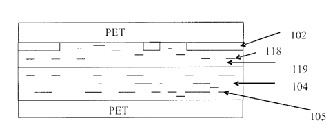
plate which is pressed
against a load roll of hot stamping foil to affix the foil to an article or
substrate. A roll on transfer
process could also be used in this invention. In this case, the article
substrate and the adhesive
(UV or heat activated) is brought together at a nip to effect the transfer of
the hot stamp layer to
the article substrate.
[10] An image is typically formed by utilizing a metal or silicone rubber die
into which the desired
image has been cut. This die is placed in the hot stamping machine and is used
to press the image
into hot stamp foil utilizing a combination of heat and pressure. The back
side of the foil is
generally coated with a dry heat activated, thermo set adhesive, for example
an acrylate based
adhesive. Upon the application of heat, the adhesive becomes tacky in regions
of the heated image
and adheres to the paper or plastic substrate.
[11] Hot stamping is described or mentioned in the United States patents
5,002,312, US 5,059,245,
US 5,135,812, US 5,171,363, US 5,186,787, US 5,279,657 and 7,005,178, in the
name of Roger
Phillips of Flex Products Inc. of Santa Rosa Ca. Additional details of a hot
stamping process may
be found on pages 440-445 of the Modern Plastics Encyclopedia, 1979-1980.
[12] Aforementioned United States patent 5,059,245 describes forming an
optical coating upon a
substrate wherein the optical coating in one embodiment comprises optically
variable flakes
applied within a carrier as paint or ink which is then dried or cured upon the
substrate.
[13] Optical effect flakes in an adhesive may have one or more predetermined
optical
characteristics; for example, flakes may be optically variable changing color
with a change in
angle of incident light, or flakes may be diffractive, or may have covert
symbols therein or
3
CA 02580321 2013-07-17
Doc No: 18-243 CA Patent
thereon, or the flakes may simply be reflective or absorptive. In some
instances, optical effect
flakes have a combination of optical effects, for example they may be
diffractive and color shifting,
or they may be diffractive and reflective, or diffractive and highly
absorptive depending upon the
desired effect. Furthermore flakes having different optical effects may be
mixed together in desired
ratios. Pigments that may be added include those based on interference, for
example mica based
pigments, Fabry Perot type pigments, liquid crystal type pigments, including
those that color shift
with viewing angle, non- shifting pigments like gold and nickel, and other
metallic flakes. Dyes and
or other pigments may be added to the adhesive to modify the colors of the
interference and /or
diffractive pigments, including covert platelets, known as charms or taggants,
and other shaped
particles. The examples of covert flakes include, but not limited to, charms
or taggants as taught in
United States patent application publication number 2006/0035080, shaped
pigments as disclosed in
United States patent application publication number 20060035080, magnetic
flakes, fluorescent
pigments, standard UV activated to form visible light, or specialized anti-
Stokes materials UV
activated to form visible light.
[14] Heretofore, in instances when a layer of material such as an ink coated
substrate having
optically variable flakes therein was hot stamped to another substrate or
object, prior to hot
stamping, a heat-activated adhesive layer, typically 2 - 20 microns thick, was
applied to the
substrate or object to adhere the layer of material to the substrate or object
by applying suitable heat
and pressure.
[15] In relation to Figs. la and lb, US Patent 7,029,745 teaches a method
of affixing a security
article, such as security article 30, to a carrier substrate 66 through a hot-
stamping process. Fig. la
shows security article 30 with a release layer 62 formed on one side of a
light transmissive substrate
24, such as an acrylic coating with an interference pattern formed thereon.
The release layer 62
allows security article 30, including substrate 24, absorber layer 18,
dielectric layer 20 with optical
interference pattern 15, and reflector layer 22, to be released from carrier
structure 64 during the
hot-stamping process.
4
CA 02580321 2013-07-17
Doc No: 18-243 CA Patent
[16] As shown in Fig. lb, the release layer 62 and carrier structure 64 are
removed when security
article 30 has been applied to an object such as a carrier substrate 66 by hot-
stamping, with security
article 30 being coupled to carrier substrate 66 by way of adhesive layer 68.
Sometimes the release
stays with the substrate 62. The bonding of adhesive layer 68 against carrier
substrate 66 occurs as
a heated metal stamp (not shown) comes into contact with carrier structure 64.
The heated metal
stamp simultaneously forces adhesive layer 68 against carrier substrate 66
while heating adhesive
layer 68 to more effectively bond to carrier substrate 66. Furthermore, the
heated metal stamp
softens release layer 62 thereby aiding in releasing security article 30 from
carrier structure 64
which is subsequently discarded. Once security article 30 has been attached to
carrier substrate 66,
the image produced by security article 30 is viewed from substrate 24 toward
optical coating 16.
[17] In the field of hot-stamping, a plurality of commercially available
adhesives have been
developed to provide required adhesion of foils to same and other materials,
under heat and
pressure. Although these heat-activated adhesives have performed their
intended function, they
have not provided additional functions now perceived to be highly useful.
[18] For example, the inventors of this invention have discovered that
these dry heat activated
adhesives can be applied to a substrate and can be preloaded or premixed into
the adhesive with
special optical effect flakes, such as magnetic flakes, magnetically alignable
flakes, magnetic flakes
with color shifting properties, color shifting -flakes, color switching
flakes, diffractive flakes and or
covert .flakes bearing indicia also known as charms.
1191 It is an object of this invention to provide a hot stamp adhesive,
that has therein, special
effect flakes, and wherein the flakes can be seen through one or more layers
the adhesive is
bonding. It was not anticipated that acceptable adhesion would result when
optically variable
pigment was added to the hot stamp adhesive. The adhesive could also be
printed in a pattern so as
to affect a patterned transfer even though a flat die would be used to make
the hot stamp transfer.
Printing the adhesive rather than having an image in the die of the hot
stamper results in a better
transferred image with higher definition without "fringe" often seen in foil
type transfers. Fringe
refers to the ragged edges of the foil image when hot stamped onto surface of
CA 02580321 2013-07-17
Doc No: I 8-243 CA Patent
paper, for example. The problem is evident often in the hot stamp transfer of
the letter "A" where
the triangle of the letter "A" is covered with foil.
[20] It is an object of the invention, to provide a Chromagram where the
provision of a discrete
special effect layer is obviated, by adding special effect flakes to a hot-
stamp adhesive for to bond
two objects together. This makes for a product that easier to manufacture and
reduces
manufacturing costs.
[21] It is an object of this invention to hot stamp a substrate to another
substrate or object,
wherein optical effect adhesive bearing optical effect flakes is solely used
as an adhesive.
[22] Security threads have been known for some time. US Patent No.
4,186,943 to Lee describes a
windowed security thread that is contained within the banknote paper. Lee uses
diachronic coatings,
in all- dielectric optical stack, having a symmetrical design so that the same
reflected and transmitted
color and color shift is seen from either side of the paper through elongate
windows of the paper
substrate. In one embodiment, paper is removed at various points over the
embedded security thread
to allow the thread to be more clearly seen. Furthermore, unfortunately,
counterfeiters have at their
disposal from the packaging field commercially available transparent film made
from hundreds of
alternating layers of polymeric films that display similar color shifting and
reflection and
transmission characteristics as found in '943. This makes foils based on all-
dielectric suspect as an
anti-counterfeit system.
[23] Patent application publication number US20060255586 by Lazzerini
describes a security
device composed of holographic regions with a continuous metal layer of
aluminum but with
variations in its thickness. In co-pending application, W02004014665 by
Lazzerini, the method of
"thinning" the deposited aluminum is by chemical etching after some areas of
the aluminum are
protected by a transparent ink adapted to preserve the aluminum by the attacks
of acid substances.
The aluminum is thinned from an optical density of 1.8, transmission of 1.6%,
down to 0.7 optical
density or about 20% transmission, in the "A" portion, item 3 of the '586
patent application. In other
words, the aluminum is opaque in areas other than the "A" portion and only
semi-transparent in the
areas. The use of magnetic elements in register with the holographic elements
is mentioned but
6
CA 02580321 2007-03-01
Doc No: 18-243 CA
Patent
does not indicate the nature of the magnetic elements. Another version of the
invention uses color
shifting ink between the backing layer of Polyethylene Terephtalate (PET) and
the continuous
aluminum metal layer. The type of color shifting ink is not defined ¨ they
could be mica based
transparent color shift with angle pigments, or liquid crystal color shift
inks both of which are
transparent ¨ in our invention the pigment is opaque). At any rate, Lazzerini
does not teach a color
shift material based on Optically Variable Adhesive (OVA), does not have color
shift from both sides
of the security thread, does not have covert charms, and has no-demet areas in
the holographic regions
and does not have magnetic elements confined within the color shift pigment.
1241 US Patent No. 7,054,042 to Holmes et al, hereinafter referred to as
'042, disclosed a
device employing a demet hologram with a thin film color shifter underneath.
The use of a thin
film interference filter has a large drawback in terms of color control
because the methods
employed, vacuum deposition methods, particularly, those that are of such
running speeds to
make them commercially viable has at best a plus/minus 2% error on the
dielectric layer
thickness. For a Fabry Perot structure as discussed in '042, a typical design
would be Al
opaque/Low index ie. MgF2/absorber Cr 3nm. With a 2% variation for a 4 QW
optical
thickness at 550nm, this thickness variation translates into a delta E color
of 27 units and at 6
QW optical thickness at 550nm translates into a delta E color of 31. From a
practical point of
view, this color variation makes the distinction between the genuine product
and a counterfeit
problematical. The only hope to improve the color of a foil with a vacuum
process is to have
extensive editing which only leads to high a high expensive product.
1251 US Patent No. 5,700,550 to Uyama teaches the use of an all dielectric
optical stack on a
holographic forming layer, which has even less control of color than '042,
since the structure
disclosed by Uyama has five layers of alternating ZnS and MgF2 or TiO2 and
Si02. Each layer
is subject to a 2% variation which would result in even larger color
variation. Uyama also
requires that the device be placed on a black background otherwise if placed
on a white
substrate the transmissive nature of his device will result in light beams
combining from light
reflecting from the substrate back through the device with the reflected light
beam from the
interference stack to produce white light again. Even if the substrate (i.e.
currency paper were
colored) the light recombination would give low chroma.
7
CA 02580321 2007-03-01
Doc No: 18-243 CA
Patent
[26] The aim of this invention is to eliminate the drawbacks of the prior art
so that a new
security device having the desired characteristics of a thread for banknotes
or other paper
documents or even a plastic document have a layered system of counterfeit
deterrence that can
be manufactured with high quality of color control, along with visible and
covert features as
well protection for durability on both sides of the device while maintaining a
minimum
thickness. Therefore, the problem that is being addressed is to provide a new
security thread
with enhanced features that can easily be assembled. The problem is solved by
giving the
viewer security features that can be remembered, that has a distinct color
shift and covert
features for machine or forensic analysis.
[27] It is an object of the invention to provide a simplified mutli-layered
security device using
an optically variable adhesive (OVA).
[28] It is an object of the invention, to provide a thin asymmetric security
thread displaying
different optical effects when viewed from different sides.
1291 It is another object of the invention, to provide a thin security device
with high chroma
and high color control.
[30] It is another object of the invention, to provide a thin security
thread comprising a demet
hologram and covert taggents therein.
[31] It is another object of this invention, to provide a hot stamp image
with multilayer
security features.
SUMMARY OF THE INVENTION
[32] In accordance with this invention a structure for providing an optical
effect is provided,
comprising a first substrate and a second substrate affixed to the first
substrate by an adhesive
alone, wherein the adhesive comprises an energy activated binder having a
plurality of particles
8
CA 02580321 2007-03-01
Doc No: 18-243 CA
Patent
distributed therein or thereon for providing the optical effect detectable
through the first
substrate.
[33]
It should be understood the second substrate can be any object to which the
first substrate
can be affixed, for example by hot stamping.
1341 In accordance with another aspect of the invention, a method of forming
an article for
providing an optical effect is provided comprising the steps of:
a) providing a first substrate having at least a first optical effect;
b) coating the first substrate with a carrier vehicle having optical effect
particles
therein or thereon, wherein the particles provide a second optical effect
detectable
through the first substrate; and
c) hot stamping the coated first substrate to a second substrate or article so
that the
carrier vehicle is solely used as an adhesive in the hot stamping.
BRIEF DESCRIPTION OF THE DRAWINGS
[35] Exemplary embodiments of the invention will now be described, in
conjunction with the
drawings, in which:
[36] Fig. la is a schematic view of a security article before hot-stamping,
according to the
prior art.
[37] Fig. lb is a schematic view of a security article shown in Fig. la hot-
stamped to a carrier
substrate, according to the prior art.
[38] Fig. 2 is a cross-sectional view of a foil in accordance with the
invention shown before
transfer to an object wherein a substrate having a patterned Al layer has a
dry hot stamp
adhesive bottom layer having optically variable pigment (OVP) or optically
variable magnetic
pigment dispersed within the adhesive.
9
CA 02580321 2007-03-01
Doc No: 18-243 CA
Patent
1391 Fig. 3 is cross-section of a Chromagram with optically variable adhesive
after hot stamp
transfer onto a paper or cardboard substrate.
1401 Fig. 4 is a plurality of different views of a same banknote having a
hologram bonded to a
note substrate having optically variable adhesive as the hot stamp adhesive.
1411 Fig. 5 is a cross-sectional view of a Chromagram with optically
variable adhesive and
high index layer before hot stamp transfer.
1421 Fig. 6 is a cross-sectional view of a Chromagram with optically
variable patterned
adhesive.
1431 Fig. 7 is a cross-sectional view of a tamper evident device before hot
stamping.
[44] Fig. 8 is a cross-sectional view of the tamper evident device shown in
Fig. 7, after hot
stamping.
[45] Fig. 9 is a cross-sectional view of the tamper evident device shown in
Fig. 7, after
attempted removal.
[46] Fig. 10a is a cross-sectional view of a Chromagram structure showing
color shift hot
stamp adhesive with an over-layer of adhesive containing covert taggants.
1471 Fig. 10b Security thread constructed from OVA and roll-on transfer of
demet hologram
using two different OVA layers.
1481 Fig. 11 is a cross-sectional view of a Chromagram structure showing
patterned aluminum
with a color shift hot stamp adhesive and a separate top layer of adhesive
containing covert
platelets.
CA 02580321 2007-03-01
Doc No: 18-243 CA
Patent
[49] Fig. 12a is a cross-sectional view of a Chromagram structure according to
one
embodiment of the present invention.
[50] Fig. 12b is a cross-sectional view of a Chromagram with an adhesive
between an
optically variable (OV) foil and demet hologram.
[51] Fig. 12c is a cross-sectional view of a Chromagram with a clear
adhesive between the foil
and demet hologram, wherein the adhesive contains covert flakes or a low
concentration of
optically variable flakes or optically variable magnetic flakes.
[52] Fig. 12d is a cross-sectional view of a Chromagram with an adhesive.
1531 Fig. 13 is a cross-sectional view of a thin color shifting security
thread.
1541 Figs. 14 and 15 are graphs used to calculate formulas for estimation of
the amount of
deposited pigment.
1551 Figs. 16 and 17 are graphs depicting reflectance scans of hot stamp
transferred images.
1561 Fig. 18 is graphical representation of the subtractive absorbance
data.
[57] Fig. 19 is a graph of cross web optical density measurements.
[58] Fig. 20 is a photograph of a security device applied to a casino chip
through a hot stamp
transfer adhesive process.
[59] Fig. 21 is a cross-sectional view of a refined "synthetic thread"
wherein multiple optical
effects are produced by a layered security system.
[60] Fig. 22 is a set of photographs of a security thread according to the
present invention.
11
CA 02580321 2007-03-01
Doc No: 18-243 CA
Patent
[61] Fig. 23 is a cross-sectional view of a Laminate Security Thread using OVA
according to
one embodiment of the present invention.
[62] Fig. 24 is a cross-sectional view of a security thread wherein at
least three layers of
adhesive are used to laminate two substrates.
[63] Fig. 25 is a cross-sectional view of a security thread wherein a
substrate is laminated
using two different OVA's.
DETAILED DESCRIPTION
[64] For the purpose of this application, the term "energy activated
adhesive" or "energy
activated binder", means a bonding substance that requires an energy source
for curing. The
energy activated adhesives include, but are not limited to, hot stamp
adhesives, UV activated
adhesives, thermoplastic and thermoset adhesives, paint¨based polymeric
compositions,
varnishes, and staining compositions. By way of example, an adhesive is
selected from the
group of: polymethacrylate, polyacrylate, polyamide, nitrocellulose, alkyd
resin, polyvinyl
alcohol, polyvinyl acetate, and polyurethane.
[65] The methods of activating the adhesives include hot stamping, UV curing,
applying heat,
or a beam of electrons. For brevity, an energy activated adhesive, possibly
with special flakes
therein, is referred to as "an adhesive" hereinbelow where it does not lead to
confusion.
1661 As was described heretofore, in the background of the invention, the
field of hot stamping
and more particularly, hot stamping of one optical coating or substrate with
another is well
known. For example, coated substrates bearing images, logos or other indicia
are hot stamped
onto lottery cards, passports, banknotes, driver's licenses, poker chips, and
a variety of other
articles and substrates are well known.
[67] Although commercially available hot stamp adhesives are known to perform
their
intended function, the inventors of this invention serendipitously discovered
that some cured
paints having optically variable flakes therein serve adequately as hot stamp
adhesives. Note,
12
CA 02580321 2007-03-01
Doc No: 18-243 CA
Patent
that the paint is no longer a paint but is now an adhesive thereby obviating
the requirement or
step of adding an adhesion layer of material to a paint layer having optically
variable properties.
Furthermore, the added benefit of having special effect flakes within the hot
stamp adhesive
provides enhanced structures. As well overall thinner structures may result
from this method, as
well as structures with a patterned adhesive layer, and structures comprising
more than one
layers of adhesive providing different optical effects, for example having
charms in one layer,
and OVP in another.
1681 The adhesive may be printed into patterns or flood coated over the
entire surface. If
patterned, the product becomes more tamper proof since the product cannot be
physically
removed in one piece. Attempts to remove the device by dissolving the adhesive
using solvents
would also be detrimental since the solvent would also attack the
hardcoat/release which in turn
would destroy the device, making tampering obvious.
[69] The flakes may vary considerably in size, but are preferably at least
5 microns in
diameter or across their surface. Flakes can be optically variable flakes,
color-shifting flakes,
thin film light interference flakes, diffractive flakes, reflective flakes,
light absorbing flakes,
covert flakes, flakes bearing symbols or indicia, flakes that are uniform in
shape, and magnetic
flakes, color shift pigments, such as thin film metal-dielectric, all
dielectric, mica based
pigments, liquid crystal pigments etc.
[70] The inventors also discovered that flake material such as optically
variable, diffractive,
absorptive, or reflective flakes or flakes having other properties such as
covert features, can be
added directly to conventional hot stamping adhesives prior to curing to
provide both the
benefits of adhesion and the optical effects which the added flakes exhibit.
[71] Some of the devices described in this application comprise a light
transmissive or
essentially transparent substrate, which may be made of Polyethylene
Terephtalate (PET),
Oriented Polypropylene (OPP) or other suitable plastic material. By way of
example, a PET
layer has a thickness of 6-25 microns. It should be understood that when the
description of a
device contains only one substrate, a second substrate can be a protective
coat, a release coat, or
13
= CA 02580321 2013-07-17
Doc No: 18-243 CA Patent
any document or object to which the first substrate can be affixed, by way of
example a paper
document or a free standing plastic film.
[72] An optical stack, also referred to as an interference stack, comprises
a reflective layer, an
absorber, and a dielectric layer between the reflective layer and the
absorber, as it is known in the
art. A reflective layer can be made of any metal that has a reflectance over
20%, preferably
aluminum. By way of example, a dielectric layer is made of MgF2 or other
transparent material as
known in the art.
[73] An absorber can be a grey metal with a ratio of n/k about 1, where n is
the real part of the
refractive index and k is the imaginary part of the reflective index, for
example Cr, Ti, or Ni, or can
be a non-selective absorber across the visible spectrum like TiN, or can be a
cermet, as described in
the article entitled "Influence of Nanosized Metal Clusters on the Generation
of Strong Colors and
Controlling of their Properties through Physical Vapor Deposition (PVD)" by R.
Domnick et al.,
49th Annual Technical Conference Proceedings (2006), Society of Vacuum
Coaters. By way of
example, a cermet material comprises silver islands in a dielectric matrix.
[74] Some of the devices disclosed in the present application comprise a
diffractive structure,
which may be any relief including a hologram, a demetallized hologram, a
kinegram, and a zero
order diffractive structure or a simple grating structure. An embossable resin
can be made of such
materials as type G PET, Polycarbonate, polyvinyl chloride or
polymethacrylate. An embossable
layer may be combined with hardcoat/release layer. An embossing may be either
patterned or
continuous. A demet layer can be made of Al, Cu, Ni, and other metals and
metal alloys that has
been patterned by demetallization. Various techniques may be used to pattern
the metal layer, such
as chemical etching or oil ablation in vacuum, both done in registration with
the relief image. A
high refractive index layer can be made of ZnS, Ti02, Zr02, etc.
[75] In one embodiment of this invention, dye particles are added to the
adhesive to modify the
optically variable effect. Optionally, the adhesive layer is transparent or
semi-transparent and
concentration of the pigment particles is adjusted so that when a security
article
14
CA 02580321 2007-03-01
Doc No: 18-243 CA
Patent
is hot stamped to a printed document, the insignia printed on the document is
visible through the
security article.
1761
In one embodiment of this invention, colorless reflective flakes are added to
the adhesive,
so that the flakes appear to have color, reflecting the color of the dye in
the adhesive or paint or
ink used as adhesive, wherein the ink is preferably made of acrylic or
urethane carrier with
flakes therein.
[77] Another embodiment of this invention is a single layer of adhesive
with particles
providing an optical effect therein. By way of example, the particles are
color-shifting flakes.
This structure can be used to join two objects together, wherein one of the
objects is light-
transmissive to make visible optical effects provided by the adhesive.
[78] In another embodiment of the present invention, reflective flakes
bearing symbols or text,
as described in co-pending US Patent Application publication number
20060035080, are added
to the adhesive. These symbols stand out against a colored background when
viewed under a
microscope using reflected light.
[79] In another embodiment of the present invention, a security device
comprises two
adhesive layers: a first layer of adhesive is dye-free and has reflective
flakes therein; a second
layer of adhesive is colored with a dye, so that the dye mutes or enhances the
reflectance of the
first layer, depending from which side the security device is viewed.
[80] In other embodiments of the present invention fluorescent dyes activated
by UV or up-
conversion pigments that fluoresce when IR activated, for example by two
photon absorption,
are added to the adhesive as a covert feature. Nano-particles or transparent
conductive particles,
for example Indium Tin Oxide (ITO) flakes, can also be added to the adhesive
for covert
features.
[81] In a less preferred embodiment of the present invention, an adhesive
is first applied to a
substrate and then optically variable pigment (OVP) particles are added to the
adhesive, for
CA 02580321 2007-03-01
Doc No: 18-243 CA
Patent
example, sprinkled or scattered by an air jet onto the adhesive surface,
optionally followed by
more adhesive so that a semitransparent layer of OVP is seen in the
transferred product.
1821 Although a stamping die may be utilized in some embodiments having an
image formed
therein, alternatively an image may already be created in the form of a de-
metalized hologram.
In this instance, a flat hot-stamp die is utilized to transfer the image. The
transferred image may
be a square or other shape as defined by the flat hot die or by the area of
the adhesive.
1831 An alternative to the hot-stamping an adhesive onto a demetalized (demet)
hologram, is
to print a UV activated adhesive containing the OVP particles, bring a
laminating sheet
containing the demet hologram onto the adhesive and then cure the adhesive by
shining the UV
light or e-beam radiation through the transparent backing to the adhesive
sheet or e-beam
radiation though the demet hologram using the e-beam curing step. UV will not
work through
the areas of the hologram that are not demet unless the width of the non demet
areas are very
narrow, estimated to be less than 2 microns, so that the UV can cure the
adhesive by coming in
at an angle.
[84] Fig. 2 shows a structure in accordance with one embodiment of the present
invention. An
embossed hologram layer 100 has an Al layer 102 thereon. The opaque Al coating
102 is
patterned to form windows or gaps. Both the opaque Al regions 102 and gaps
therebetween are
coated with optically variable adhesive 104 having therein optically variable
flakes 105, which
can be magnetic pigment flakes shifting color with viewing angle. A resin
layer 106 is formed
to allow the embossing of relief surface 100, and a release (or hardcoat)
layer 108 is coated onto
the removable carrier substrate 110, typically PET 10-25 microns in thickness.
In another
embodiment, the release and hardcoat/resin layers are combined into one layer.
[85] Fig. 3 shows the structure of Fig. 2 hot stamped to a paper or
cardboard substrate 112.
When the PET layer 110 is removed and the structure is viewed from the top
looking down
through the hard coat 108, through the holographic patterned Al layers, color
shifting coating is
seen through the windows. What makes this structure particularly ideal is the
synergy that is
attained by combining special effect pigments in the adhesive material,
obviating the
16
CA 02580321 2007-03-01
Doc No: 18-243 CA
Patent
requirement for an additional thick color shifting layer. The overall
thickness is less than 20
microns, typically around 10 microns.
[86] Fig. 4 is a photograph of a portion of a Chinese note, wherein the
structure shown in Fig.
2 is hot stamped to the banknote paper. This structure includes a hologram
made by Hologram
Industries of Paris, France, and provides color shifting effects, i.e.
different colors can be seen
from different angles. For example, a square background changes its color from
indigo, pointed
by arrow 301, through violet - arrow 302, to hot pink color, pointed by arrow
303.
[87] The hot-stamped (HS) product has higher chroma than its ink counterpart
because the
flakes settle fast in the low viscosity formulation adhesive against a smooth
substrate. Printed
OVP has a lower chroma because one is looking at the side of the ink that was
pulled away from
the applicator. When a string of ink breaks, clumps of ink flow out a
relatively rough surface
compared to interface between a plastic substrate and ink. This is why the HS
has better chroma
than a printed surface.
[88] The device shown in Fig. 4 has at least five security elements: 1) a
hologram with a
double image - the number "25" in the center of the hologram appears at one
angle and
disappears at other angles, 2) an image of Venus de Milo that is easily
remembered. 3) the
hologram has a demetallized Al layer in a lace pattern, 4) a color shift, and
5) covert images
seen at 100X or higher magnification.
[89] An alternative embodiment of the invention is shown in Fig. 5 wherein a
high refractive
index layer 114 is coated between the optically variable adhesive layer 104
and the Al patterned
layer 102. The high refractive index coating 114 of a material such as ZnS,
TiO2 or Zr02 is
coated over the demetallized holographic film. In this instance, the high
index layer 114 allows
the diffractive or holographic surface 100 to be seen at the same time as the
optically variable
adhesive 104. The high refractive index prevents an optical index match
between the adhesive
and the embossing in the resin layer.
17
CA 02580321 2013-07-17
Doc No: I 8-243 CA Patent
[90] An alternative embodiment is shown in Fig. 6, wherein the optically
variable adhesive 104
is printed between the windows of the aluminum 102 so that the transferred
device will be tamper
evident. If one tries to remove the device, it will break apart in regions
defined by no adhesive and
with adhesive.
[91] According to another embodiment of the present invention shown in Figs. 7
¨ 9, a device
has a patterned release layer 108 on a substrate, resin layer 106 with high
adhesion to the substrate,
and is coated continuously across the windows and non-windows of demet
aluminum layer 102
with an OVP adhesive 104 with flakes 105 therein. Fig. 7 shows the device
before hot stamping it
to carrier 66 which needs protection. In operation, the device is attached to
the surface 66 as shown
in Fig. 8, wherein adhesive 104 is activated by hot stamping. If someone tries
to detach the device
from the carrier, the release layer 108 only releases in a pattern, leaving a
reverse pattern on the
substrate 66. The result of such attempt is shown in Fig. 9, wherein the
broken jagged split of
adhesive is pointed by arrow 120. In effect, this device is a tamper evident
security label.
[92] The following embodiments of the present invention are Chromagrams having
two different
layers of optically variable energy activated adhesive for providing at least
two different optical
effects, wherein one of the adhesives may contain covert taggant flakes,
referred in the art as
taggants or taggents.
[93] In the embodiment shown in Fig. 10a, a Chromagram comprises a hologram,
that may be
demetalized, or a high index layer, or other relief type surface, and the
adhesive made up of two
discrete layers. One of the hot stamp adhesive layers, layer 119, contains
covert materials, in this
instance covert flakes 118, and the other hot stamp adhesive 104 contains
optically variable
pigment 105. This invention provides a vehicle for efficient use of expensive
covert materials. The
examples of covert flakes 118 include, but not limited to, charms or taggants
as taught in United
States patent application publication number 2006/0035080, shaped pigments,
magnetic flakes,
fluorescent pigments, standard UV activated to form visible light, or
specialized anti-Stokes
materials IR activated to form visible light. The covert materials are placed
in a thin layer of
adhesive 119 covered by a layer of adhesive 104
18
CA 02580321 2007-03-01
Doc No: 18-243 CA
Patent
containing color shift pigments, such as thin film metal-dielectric, all
dielectric, mica based
pigments, liquid crystal pigments etc. The covert materials are not visible
under normal
condition, but easily detectable, for example, in UV light, or under a
microscope, or by
magnetic or infrared detectors. Upon application of the Chromagram to a
document or other
object requiring protection, the PET layer having a thickness of 12-25
microns, typically 19
microns, is discarded leaving a very thin security device on the document, no
more than 20
microns thick.
[94] An alternative embodiment of the invention is shown in Fig. 11. A
patterned Al layer 102
on a PET substrate is laminated to another PET substrate that has been coated
with optically
variable adhesive. The aluminum pattern may take the image of text, symbols,
bar-codes or even
photographic images. The aluminum is patterned by means of a demet process
(laser ablation,
chemical etch, or oil ablation of a flexographic print image in a vacuum
machine). In the case of
photographic images produced by using the oil ablation process resolutions
down to 70 microns
(,-,180dpi) can be achieved. Oil ablation is the demet method of choice since
the patterned
aluminum takes places in line, in vacuum, in one process step. The optically
variable adhesive
comprises at least one of two discreet layers of adhesive, one adhesive layer
104 contains color
shift pigments 105 and another adhesive layer 119 contains covert materials
118. This forms a
security thread. In this case, the thickness of the PET layers is about 5-10
microns each, so that
the overall thickness is 20 microns or less. This thickness limitation is
necessary for a security
thread so that in a stack of banknotes one end of the stack is not thicker
than the other end.
1951 In another embodiment of the present invention shown in Fig. 10b, a
two coat process is
utilized to laminate two transparent substrates together. First, a demet
hologram is coated by
successive layers of optically variable adhesive: a first coat of an optically
variable adhesive 130,
either magnetic or non-magnetic, and a second coat of a different optically
variable adhesive 131.
By way of example, the first coating shifts color gold-to-green, and the
second coating shifts blue-
to-red. Then a substrate 110, transparent or semi-transparent, is laminated
via a hot nip roller to
the adhesive 130. After that, a second substrate supporting the hologram (not
shown) is removed
leaving protective layer 106. The final product has different color shifting
effects dependent on
19
CA 02580321 2007-03-01
Doc No: 18-243 CA
Patent
which side it viewed from. In yet other embodiments, one of the coatings is
non-shifting, and/or
contains covert features.
[96] In reference to Fig. 11, an additional embodiment of this invention is
a structure wherein an
optically variable adhesive is used to laminate two pieces of transparent PET
to produce a color
shifting security thread. Looking at one side of such a structure, in Fig. 11
from top down, one
would see the image formed by the demet hologram and a color shift in addition
to the covert
images e.g. fluorescent. From the other side, one would only see a color shift
if the opaque
pigments were used at high concentration. For example, interference based
metal-dielectric
pigments at concentrations greater than10% of pigment weight in total solids -
pigment plus
adhesive produce such an effect. In this embodiment, a release layer is
absent, and the patterned
metal layer and the covert images are optional.
[97] In one embodiment of the present invention, an adhesive with color
shifting flakes therein
is used as a laminate adhesive to make a security thread that is thin and has
qualities of an
optically variable device (OVD). By way of example, a 6-10 micron thick web is
coated with
the optically variable adhesive (OVA), which is a thermoset adhesive or a
moisture cure
urethane adhesive with OV particles therein, and laminated at a hot nip to
another 6-10 micron
thick web to produce a laminate sheet. This sheet is then slit for security
ribbons having 2-5mm
in width, which are typical widths used for currency. In essence, it creates a
synthetic foil due
to the low viscosity of the adhesive during the first coating operation and
then again during the
nip process. Both processes tend to align the flakes flat with the web
surfaces.
[98] In one embodiment of the present invention a transparent substrate, for
example made of
PET, with dye added to add or suppress colors of the optically variable
adhesive, disposed on the
substrate, and printed information is added to the substrate layer.
Optionally, a demet
Chromagram is roll nipped to the adhesive layer.
[99] According to another embodiment of the present invention, the structure
shown in Fig. 12a
has resin layer 106, embossed with relief 100, but has no release layer.
Relief 100 is covered with
demet aluminum 102 and two layers of adhesive 104 and 119 with different
flakes 105 and 118.
CA 02580321 2007-03-01
Doc No: 18-243 CA
Patent
By way of example, flakes 119 are covert flakes, taggants, and flakes 105 for
providing a color¨
shifting effect. Alternatively, substrate 110 itself can be an embossable
layer. Such materials as
type G PET, Polycarbonate, polyvinyl chloride or polymethacrylate are suitable
for embossable
substrate 110. This structure would be useful as a security label, so that
layer 104 would be
attached to the outside of a box or package.
11001 In one embodiment of the present invention, a demet hologram is first
coated with
charms in an adhesive, followed by an additional hit of adhesive with OVP
therein. This double
hit method utilizes fewer charms and makes the charms more visible, than known
in the art
methods, wherein charms are disposed throughout the optically variable ink
medium and many
of the charms are screened out by the overlaying OVP opaque particles.
Preferably, the OV ink
has an acrylic or urethane carrier.
[1011 In one embodiment of the present invention, the first adhesive layer is
discontinuous. By
way of example, a first thin layer of adhesive carrier with relatively low
viscosity is printed onto
a substrate in form of dots. The carrier contains a high density of charms or
other flakes therein,
and is covered with a second layer of less expensive adhesive providing an
additional optical
effect.
[102] In another embodiment shown in Fig. 13, the structure is composed of a
PET layer 110, an
optional resin layer 106 with embossing, a demet Al layer 102, two layers of
adhesive 104 and
119, and a protective hardcoat covering layer 108, i.e. the protective
hardcoat/release takes the
place of the second PET. In this way, the overall security thread type
structure can be made quite
thin, for example, 15 microns even if a 9 micron PET is used for embossing or
for depositing an
embossing lacquer/resin 106. By way of example, this structure is made by
running a PET with a
demet hologram or a PET just with patterned Al, through a heated nip against a
releasable PET
coated with the layers of adhesive containing the color shift materials and
the covert materials.
The releasable PET is later discarded, but hardcoat layer 108 stays with the
final structure as
shown. Alternatively, a demet hologram on a PET substrate is processed
serially through a
number of gravure print stations including two print stations for the adhesive
119 and 104 and a
print station for the protective hardcoat. Drying stations are placed between
each print station.
21
CA 02580321 2007-03-01
Doc No: 18-243 CA
Patent
11031 In the embodiments described hereinafter, an OV foil has a demet
hologram in a region
thereof with an OV adhesive between the foil and demet hologram.
11041 In another embodiment shown in Fig. 12b, first substrate 222 is coated
with a reflective
layer 220a, a dielectric layer 220b and an absorber layer 220c forming an
optically variable color
shifting foil 223. Substrate 212, which can be a resin/hardcoat layer, is
impressed with a hologram
and partially coated with a pattern of highly reflective aluminum 216 in
register with the
hologram, for preventing light from passing therethrough. As a result,
substrate 212 has one or
more regions 100 embossed and covered with demet aluminum. Substrate 212
optionally has one
or more regions 214 embossed but not covered with aluminum. Resin layer 212 is
optionally
covered with protective light transmissive layer 218 with opaque indicia 219
printed thereon. The
demet hologram is hot stamped or hot roll nipped to the optical stack using
clear hot stamp
adhesive 230.
11051 Shown in Fig.12d, a layer of adhesive with OV particles can be used as
shown in another
embodiment shown in Fig. 2d. This embodiment is similar to shown in Fig. 12b
in many respects,
however has a first substrate, preferably made of PET, coated with a color
shifting flakes 235 in a
carrier 234, an adhesive or acrylic- or urethane-based ink, hot stamped to the
same upper structure
as in Fig. 12b. After the ink has dried and cured, thus forming a color
shifting coating, a hot
stamp adhesive 230 is applied and cured. To form a Chromagram the coated first
substrate having
the hot stamp adhesive 230 is bonded with a second substrate covered with the
same layers as in
the embodiment shown in Fig. 12b.
11061 In another embodiment shown in Fig. 12c, covert flakes 245 bearing
indicia that cannot
be seen with the unaided eye are mixed into the hot stamp adhesive 240 and are
used to bond the
two structures together as in the previous embodiments. In this embodiment
both color shifting
effects that can be seen though the windows where the Al coating is missing
and with
magnification the covert flakes 245 can be seen and serve as a means of
authentication. Instead
of covert flakes, optically variable flakes could be used at low
concentrations so that the OV foil
colors are modified when viewing from the top.
22
CA 02580321 2007-03-01
Doc No: 18-243 CA
Patent
[107] This manufacturing process allows the first and second substrates to be
manufactured in
two different facilities and stored in rolls to be united later.
[108] The present invention was reduced to practice as follows: The adhesive
was diluted to the
correct strength by the addition of toluene and applied using a reverse
gravure coater equipped
with in-line drying ovens. The applied adhesive levels ranged from 1.5-10 g/sq
m while the
pigment applied was between 0.005 and 0.05 g/sq m for the covert pigment and 1
-10g/sq m for
color shift OVP pigment. Two optically variable pigments were chosen for a
series of devices: a
red to green two period stack i.e. Ab/D/Ab/D/R/D/Ab/D/Ab and a Blue to Red a
one period
optical stack i.e. Ab/D/R/D/Ab, where Ab is an absorber of Cr, D is a
dielectric of MgF2, and R is
a reflector of aluminum. Two different covert charms were used: a 10 micron
square shaped
pigment with a à symbol located in its center and a 30 micron square shaped
pigment with a $
sign in its center. The press speed was about 20 feet/min for each.
Experimental Results
[109] Experiments were preformed by incorporating optically variable pigment
(OVP) into a
commercially available hot stamp adhesive. The thickness for hot stamp
adhesive was between
31.im and10 lam, with preferable range 3- 7 [im.
[110] Formulas were developed to estimate pigment deposition weight of applied
pigment to
hot-stamp adhesive (HSA) coating from their optical density. It was found that
in general the
optical density of a pigment/HSA should be approximately 0.3 or greater on a
black background
to obtain optical performance that approaches coatings with an optical density
of approximately
0.6 on a white background.
11111 In test trials, a series of hot-melt adhesive and pigmented hot melt
adhesive blends were
coated on 19iim polyester film with a release layer and Chromagram layer.
[112] The adhesive coating was carried out on a 10" wide solvent roll coater
with 100 feet of
drying oven. The adhesive was applied by reverse roll gravure.
23
CA 02580321 2007-03-01
Doc No: 18-243 CA
Patent
[113] Pigments were blended into a commercial hot-melt adhesive and stirred
continuously
until placed in the coating pan. Toluene was used to dilute formulations to
obtain the lower
coating weight samples. The sample for percent solids was taken from the
adhesive just before
it was added to the coating pan. The adhesive application weight was obtained
by weighing a
known area of coated web, removing the adhesive with solvent, drying the web,
and weighing
the web after the adhesive was removed. Three samples across the web were
taken for each
coating weight and averaged to obtain a coating weight for each sample. Anilox
rolls were
cleaned after each sample was run. A 75 TH (Trihelical) Anilox roll was used
for the majority
of the experiments. A 55 TH Anilox roll was used with two coatings to increase
the amount of
deposited adhesive.
[114] The first 4 coatings were un-pigmented applications coated at two
different dilutions.
These coatings were used to determine the optimum coating weight for
acceptable hot stamp
transfer. It is known in the art that the adhesive thickness can vary in a
very broad range. By
way of example, conditions that yielded an un-pigmented adhesive thickness of
31,tm ¨ 3.5p,m,
calculated from g/m2 measurements, were chosen to yield the optimum adhesive
coating
thickness.
[115] Each of the coated web samples was evaluated for stamping performance
and optical
density. Hot stamp transfers were made of all the samples. The optimum
stamping conditions
for transfer were found to be 100 C to 125 C, 0.5-1.0 second dwell time,
using the Kenson Hot
Stamp Press with the 35 mm x 22 mm rectangular brass stamp. The pressure was
adjusted to its
lowest operational point to minimize embossing of the evaluation samples. Very
little fringing
was observed with any of the samples. Hot stamp transfers of each of the
samples were made
onto the black and white areas of Leneta cards. The transfers were made at 100
C, 1.0 sec.
dwell time. Reflectance scans and color variation measurements were made over
the black and
white backgrounds for each transfer.
[116] Optical densities were measured over the transparent areas of the web.
24
CA 02580321 2007-03-01
Doc No: 18-243 CA
Patent
[117] Tables 1 and 2 summarize the adhesive coated web properties.
11181 The optical density (OD) of the pigment-containing adhesive was used to
estimate the
amount of pigment on the web. This was done to determine if this could be used
as a viable
analytical procedure for setting a production specification for the
adhesive/pigment deposition.
If the ratio of pigment to adhesive is known for any formulation, the optical
density of the
adhesive coating could be used to determine the amount of adhesive applied to
any transparent
web. The optical density of the High Red vs. weight per unit area of High Red
was plotted in
Fig. 15; this dependence was used to obtain the formula for High Red. All of
the optical
densities vs. grams of pigment per m2 were plotted in a separate graph shown
in Fig. 14, and a
second formula was obtained from this data set. The formulas are very similar
regardless of the
differences in pigment weight per unit area. It is likely that an offset
exists in the total data set
due to pigment settling and the fact that 3 of the 4 pigments tested have
similar pigment weight
per unit area. These factors may cause the formulas to yield slightly higher
pigment weights per
unit area.
11191 The resulting formulas for estimation of the amount of deposited pigment
are:
[120] Grams of deposited pigment = 0.1351465523379770 X (OD coated film) +
0.0591124749175451
11211 Grams of High Red deposited per sq meter = 0.135546396874281 X (OD
coated film) +
0.05.
[122] Table 3 compares the measured optical density of the coating with the
optical density
value calculated using the above formula. Because of relatively low variations
between OD
measured and OD calculated shown in Table 3, the optical density of the
adhesive coating can
be used to determine the amount of adhesive applied to any transparent web for
a known ratio of
pigment to adhesive.
CA 02580321 2007-03-01
Doc No: 18-243 CA
Patent
[123] Figs. 16 and 17 are reflectance scans of hot stamp transferred images
onto the white and
black areas of Leneta cards, respectively. The data shown in Figs. 16 and 17
was converted to
absorbance, and the values of absorbance related to the white areas were
subtracted from the
corresponding absorbance values related to the black areas. Graphical
representation of the
subtractive absorbance data is shown in Fig. 18. Samples that show the
smallest variation
between their black and white absorbance values have the highest performance.
The highest
performance samples are the samples with the highest pigment loading.
[124] Cross web optical density measurements are displayed in Fig. 19. There
were 5 equally
spaced measurements taken across each web. The data indicated that the cross
coating thickness
varied by less that +/- 5% in all pigmented adhesive cases.
[125] In Table 4 of experimental data, "Charm L" stands for Low concentration
of charms and
"Charm H" ¨ for High concentration of charms.
11261 Fig. 20 is a photograph of a security device applied through a hot stamp
transfer adhesive
process as described before, in which covert flakes bearing the à symbol and $
symbol are
disposed within the adhesive material over blue to red color shifting flakes
in a second layer of
adhesive. Here a poker chip has a holographic image of Venus di Milo on a
background of color
shifting flakes. The covert flakes can be seen with 100 times magnification
but are not visible
without magnification. This embodiment combines color shifting, holographic
effects and covert
symbols using adhesive bearing special effect flakes.
[127] To produce the aforedescribed chips, the adhesive coated rolls were slit
down the length to
a width of 3.25 inches so that two rolls of hologram/OVP adhesive i.e.
Chromagrams could be hot
stamped two at a time. A Malahide hot stamping machine, model, E4-PK, was used
to transfer
the Chromagrams to poker chips made of acrylonitrile butadiene stryrene (ABS)
copolymer. The
die was made of silicone rubber and was set at about 375 F.
[128] Approximately 1000 impressions were continuously printed at the
production rate of 450-
500 impressions per hour. The transfers had good adhesion when scraped with a
finger nail and
26
CA 02580321 2007-03-01
Doc No: 18-243 CA
Patent
there was very little fringing. The Chromagram foil production performance was
equivalent to
commercial hot stamp foils. In practice, the covert images would either show
the denomination of
the banknote, poker chip or the logo, symbol of the bearer or company issuing
such value based
documents.
[129] In the case of using transparent covert pigment and transparent color
shift pigment in a
transparent adhesive, an additional security element is introduced so that the
observer will also be
able to see printed information that is on the document through the device.
[130] Described hereinafter are embodiments of refined "synthetic threads"
wherein multiple
optical effects are produced by a layered security system.
[131] In reference to Fig. 21, a security thread comprises substrate 110,
reflective layer 102b,
optically variable adhesive layer 130, another layer of adhesive 132 with
charms therein, relief
structure 100 covered with demet Al layer 102a, and resin layer 106. Substrate
110 is preferably
made of PET, however oriented polypropylene (OPP) or other plastic materials
can be used. The
substrate can also be dyed in a continuous color or could be patterned.
[132] Reflective layer 102b is preferably made of Al, has windows so that
optical effect
provided by layer 130 is visible though substrate 110 and reflective layer
102b. Optionally, the
windows in layer 102b are shaped as letters or other insignia, so that a color
shifting text can be
seen though substrate 110.
11331 Alternatively, instead of the patterned layer 102b being internal to the
structure, the
substrate 110 could have the patterned layer of Al facing outward while the
internal interface of
the PET is in contact with the layer 130. In the case where the reflective
patterned Al faces the
outside of the device, an additional protective layer such a vacuum deposited
Si02 layer or an
organic resin protective layer may be placed over the reflective material.
[134] Optically variable adhesive 130 is preferably made of color-shifting
adhesive, which can
be controlled so that a color variation from one sample to another, AE,
defined as the square root
of the difference in hue squared plus the difference in chroma squared plus
the difference in
27
CA 02580321 2007-03-01
Doc No: 18-243 CA
Patent
brightness squared, is less than 1.0, using color additive mixing of the
optically variable
pigments. However, in general a AE of being less than 3.0 is acceptable to the
security field.
This degree of color control can not be achieved by optically variable foil
since color control by
additive mixing is not possible. Optionally, other materials such as
fluorescent materials,
phosphorescent and anti-stokes, dyes and other colorants can be added to the
OVA.
[135] Adhesive layer 132 having charms, taggants or pigment flakes therein, is
substantially
transparent to allow effects produced by OVA 130 to be visible therethrough;
adhesive material
of layer 132 can be clear or colored. Either the charms themselves are
transparent or the
concentration of the charms is sufficiently low to allow visibility of
adhesive layer 130.
[136] Optionally, magnetic flakes, such as metal flakes or OV flakes with a
magnetic layer
sandwiched between two layers of reflective material, are added to adhesive
within layers 130
and 132, possibly in combination with non-magnetic optically variable flakes.
[137] Relief structure 100, is embossed into the resin layer 106 covered with
demet layer 102a,
provides a demet holographic effect and includes such features as a double
image hologram, a
zero order hologram, a kinegram or other imagery based on grating technology.
Demet layer
102a is patterned to provide visibility of OVA layer, when the security thread
shown in Fig. 21
is viewed from the top. Layer 102a or 102b can be patterned with fine lines of
lace-like pattern
for providing an additional counterfeit feature, and/ or with insignia 133a.
11381 An image familiar to most people, such as famous statues of David and
Venus de Milo,
famous buildings including Eiffel Tower and Great Wall of China, famous people
like Einstein,
can be incorporated as a zero order diffractive image, allowing the common
person to recognize
and remember the device and authenticate it by combination of the image and
the associated
color shift.
[139] The thread is protected from both sides, on one side by substrate 110,
and on the other -
by a hardcoat /resin layer 106.
28
CA 02580321 2007-03-01
Doc No: 18-243 CA
Patent
11401 When the thread is viewed at one side, the top as shown in Fig. 21, a
color shifting effect
of layer 130, a double image hologram or a zero order hologram 100, a demet
lace-like pattern
of aluminum 102a with indicia 133a and covert features such as "charms", are
visible. When
the thread is viewed from another side, a color shifting pattern showing the
color shifting
background 130 in the windows of layer 102b, surrounded by reflective aluminum
102b, is
visible.
[141] Advantageously, the overall thickness of the aforedescribed thread can
be as low as 12[4
if the thread is made of 6 micron thick foil hot stamped and/or laminated to a
6 PET. Multiple
security effects within such a thin thread have previously not been achieved.
1142] Another advantage of the aforedescribed thread is multiple technologies
used to
manufacture this thread. This makes counterfeiting difficult since the
counterfeiter must have
multiple skill sets to make a counterfeit. Holographic structure, optically
variable pigment and
demet Al on the PET could be made in separate and perhaps distant facilities
and brought
together at the point of currency manufacture to make the final product. The
OVA weds all the
components together. The idea of putting components together right before the
security device
is inserted into the currency paper gives added security to the device since
interception of one
component by during shipment gives the counterfeiting only one component of
the overall
device. Optionally, said prefabricated components have matching symbols, for
example in the
aluminum layer 102b and in the demet hologram 100 and 102a.
11431 Moreover, fine lines of demet layer, such as lace-like pattern, in the
hologram make it
very difficult for a counterfeiter to reproduce the patterning using scissor,
die cutting or even
using photopolymers since precise registration is required in the demet
process to align the
demet patterns to the holographic features.
[144] Additionally, the cost of putting text or other images into the aluminum
layer next to the
PET is negligible since an oil ablation demet in-line process in the vacuum
roll coater can be
used. Resolutions down to 70t can be achieved.
29
CA 02580321 2007-03-01
Doc No: 18-243 CA
Patent
[145] Such a security thread can be used in banknotes as a windowed system
where the thread
is woven in and out the paper exposing itself in windows on either side of the
note. It can also
be embedded with in the paper itself where the paper is thin and transparent
enough over the
thread to still see the security features. Checks, passports, other security
paper documents and
plastic documents such a plastic based banknotes, credit cards and identity
cards can utilize the
aforedescribed security thread; it also can be used as a tear thread in such
items as cigarette
boxes and other secure packaging. In the case of paper documents, the viewing
from both sides
is affected by the thread passing to the surface of each side at regular or
irregular intervals or at
the same location if the paper is absent at that location.
[146] Fig. 22 shows photographs of the security thread described in reference
to Fig. 21.
[147] Fig. 23 shows a Security Thread using OVA according to another
embodiment of the
present invention. The thread comprises two light-transmissive substrates,
preferably made of
PET, joined by OVA layer 104 having optically variable flakes 105 and covert
taggants 118
therein.
[148] Another embodiment of the present invention shown in Fig. 24 is a
security thread
wherein at least three layers of adhesive are used to laminate two substrates.
The central layer
OVA comprising a carrier 104 and pigment flakes 105, and two layers of
adhesive with taggants
118 therein, the layers symmetrically disposed between the two substrates..
1149] Yet another embodiment is shown in Fig. 25, wherein a security thread
comprises
substrate 110 laminated using two different OVA's. Relief structures 100 are
covered with
demetallized Al 102 and hardcoat / resin layer 106. To manufacture such
security thread, each
side of a PET or other plastic substrate is hot stamped or roll nipped with a
Chromagram, which
is a demet hologram with OVA, wherein two OVAs differ in color and color
shifting effect.
11501 Prior art does not disclose such very thin security threads with OVA
providing a layered
system of counterfeit deterrence as described in reference to Figs. 21- 25.
CA 02580321 2007-03-01
Doc No: 18-243 CA
Patent
11511 In particular, in contrast to the aforementioned US Patent No.
4,186,943, our invention is
asymmetric so that the thread appears different from each side providing an
additional security
feature.
11521 Also, our invention improves color variation in comparison to US Patent
No. 7,054,042,
by mixing slightly different batches of optically variable pigment to get
exact color and color
shift time after time at least to less and or equal to a delta E of 1.0-3Ø
Human perception can
see color variation down to this level. Table 5 shows the variation calculated
for such a Fabry
Perot thin film foil at normal incidence using white light, for the design
comprising an opaque
Al layer, a low index MgF2 layer, and a 3nm absorber layer made of Cr.
11531 The construction of the thread disclosed in the present application also
provides a
possibility to add covert materials (covert platelets and other pigments)
which can not be done
with '042. Furthermore, although '042 mentions patterning of the opaque
aluminum it does not
result in color shifting windows in the patterned aluminum as is the case for
our invention.
Removing some of the aluminum of the Fabry Perot filter disclosed in '042,
would result in
clear windows as the cavity of the Fabry Perot is destroyed. Furthermore, the
device disclosed
in '042 is really for only viewing from one side.
11541 In comparison to US Patent No. 5,700,550, the invention of the present
application
allows for high chroma and high color control irrespective of the substrate
color to which the
device is affixed, and teaches the addition of covert taggents into the
device.
11551 In comparison to US patent Application publication number 2005/0127663,
this
invention provides better color control of the OVA and thin gauge PET as it
can easily be rolled
with an OVA.
11561 While the particular invention has been described with reference to
illustrative
embodiments, this description is not meant to be construed in a limiting
sense. It is understood
that although the present invention has been described, various modifications
and combinations
of the illustrative embodiments, as well as additional embodiments of the
invention, will be
31
CA 02580321 2013-07-17
Doc No: i 8-243 CA Patent
apparent to one of ordinary skill in the art upon reference to this
description, as recited in the claims
appended hereto.
[157] It is therefore contemplated that the appended claims will cover any
such modifications or
embodiments as fall within the true scope of the invention.
32
Table 1
CALC g per CACL g
grams
sq meter per sq in
solids per
CALC % deposited deposited
PIGMENT LINE ADHESIVE sq meter TOTAL %
PIGMENT IN pigment pigment
ROLL# COLOR
CYLINDER BCM SOLIDS deposited SOLIDS SOLIDS only only ,
'I NONE
75TH 35.5 24_00% 4.83 24_00% 0.00% 0.00
2 NONE 75TH 35.5 24.00'-'..,
5.14 , 24.00% 0,00% 0_00
'I
3 NONE 75TH , 35.5 12.00.)
3.13 12.00C-o 0.00% 0.00
4 NONE 75TH 35:3 -12,0CI..:,
2:16 12.00'..,-2 0.00% 0.00 (I)
_
w
w 5 HIGH RED 75TH 35.5 12.002::,
2.42 15.00(1,) 17.24% 0.42 0.0002692 o
N.,
, 6 HIGH RED 75TH 35.5 12.00';.:,
3.58 , 17.00% 29.41% 1.05 0_0006793 ol
co
7 HIGH RED 75TH 35.512.00.IH
4.18 20.00,2.õ) 45.45% '1.90 0.0012258' o
w
_
N.,
. 8 HIGH RED 75TH 35.5 12.0F.:,
3.95 20_00% 45.45% '1.80 0.0011584,
N.,
9 HIGH RED 75TH 35. 5 24.00%
6.55 37,00% 34.60% 2.27 0.00'14623 o
.
1-,
HIGH RED 75TH . 35.5 , 24.00% 7.18 37.00%
34_60% 2.48 0.0016030 w
1
11 BLIJEIBRONZE 75TH 35.5 12_00% 4.46 24.53% 60.00%
2.88 0_0017264 0
--.1
,
I
12 BLLIESBRONZE 75TH 35.5 24.00% 8..3 37.00% 42.86% 3.56 0.0022949
--.1-
13 JADENIOLET 75TH 35.5 24.00% 7_88 35.F.-,0% 36.84%
2.90 0.0018730
, 14 ROSE/GREEN 75TH 35.5 24.00% 8.6 41.00c..6 42.86% 3.69
_0.0023779
ROSE/GREEN 55TH 40.5 24.00% 15.69 38.00% 36_84%
5.78 0.00372941
16 ROSE/GREEN 55TH 49.5 24.00% 15.61 38.00% 36.84%
5.75 0.0037'103
.ADHES1',./E IN PAN NOT STIRRED DURINGRUN, LARGE ,AMOUNT OF SETTLING OBSERVED
ADHESIVE IN PAN STIRRED DURING RUN, NO SETTLING OBSERVED
Table 2
CALC g
per sq grams
g per sq M
meter pigment Caculated deposited
deposited per 100 g Adhesive pigment CALC OD
PIGMENT no adhesive
Thickness only for FROM
ROLL# COLOR pigment solution OD
in Microns CALC OD GRAPH
1 NONE 4.83 0 0.05
3.22 0.05 0
2 NONE 5.14 0
0.052 3.42666667
3 NONE 3.13 0
0.05 2.08666667 0
1.)
-1. 4 NONE 2.16 0
1.44 co
0
HIGH RED 2.00 2.5 0.112
0.5 0.1177732 w
1.)
1-,
6 HIGH RED 2.53 5 0.172
1 0.1855464
_
1.)
7 HIGH RED 2.28 10 0.298
1.5 0.2533196 0
1-,
w
8 HIGH RED 2.15 10 0.288
2 0.3210928 1
_
0
9 HIGH RED 4.28 12.7 0.368
2.5 0.388866 ..3
1
HIGH RED 4.70 12.7 0.396
3 0.4566392
..3
11 BLUE/BRONZE 1.78 , 18 0.408
3.5 0.5244124
12 BLUE/BRONZE 4.74 18 0.566
4 0,5921856
_
13 JADE/VIOLET 4.98 14 0.51
4.5 0.6599588
14 ROSE/GREEN 4.91 18 0.622
5 0.727732
ROSE/GREEN 9.91 _ 14 0.79
5.5 0.7955052
16 ROSE/GREEN 9.86 _ 14 0.82
6 0.8632784
ADHESIVE IN PAN NOT STIRRED DURING RUN, LARGE AMOUNT OF SETTLING OBSERVED
ADHESIVE IN PAN STIRRED DURING RUN, NO SETTLING OBSERVED
Table 3
+/- Percent
CALC g/
variation in
sq M OD
pigment FROM Measured vs. OD
Pigment only GRAPH OD
calculated 0
None 0 0.05 0.05
0 0
1.)
HIGH RED 0.417241 0 106556
0.112 4.98%
co
L., HIGH RED 1.052941 0.192722
0.172 11.36% w
1.)
HIGH RED 1.9 0 307538
0.288 6.56%
1.)
HIGH RED 1.795455 0.293367
0.298 1.57%
1-,
HIGH RED 2.266621 0 357232
0.368 2.97% w
1
0
HIGH RED 2.484632 0.386783
0.396 2.35% ..3
,
1-,
BLUE/BRONZE 2.676 0.412722
0.408 1.15% ..3
JADE/VIOLET 3.557143 0.532158 0.51 4.25%
ROSE/GREEN 5.751053 0.829534 0.79 4.88%
Table 4.
% pigment Pigment
Roll Feet Appl solids % pigment in
in Total applied to Cale % Total solids
g Coated Roll Description Adhesive formulation
g/sqM liquid ink solids web g/sqM total solids
Measured Comments
Charm L (Opaque Al Venus 400 gams adhesive +
1 150 de Milo layer of US $ charms 400 g toluene with .4 7
0.05% 0.36% 0.0071174 12% 12%-13%
applied gram US $ pigment
480.8 grams of
400 gams adhesive +
Charm L adhesive
Charm H (Opaque Al Venus
400 g toluene with
mix + 159.9g
2 450' de Milo layer of US $ and _ m 1.5 0.33%
2.33% 0.0349182 12%
1).6693 total gra
adhesive + 159.9
R.
Euro mixed charms applied
Euro +$piomentro ams toluene +
o
.98 US$ -1 1.44Euro
N.)
ix
co
o
High Red .50D adhesive on 120 g high red in
w
3 50' 7.965 13.04%
33.33% 2.66 39.13% N.)
(...) Opaque Al Venus de Milo 800 g adhesive
1-,
o.= n.)
o
High Red .80D Adhesive on 350 high red in 800 g
1-,
4 50' 10.6 30.43%
59.32% 6.29 51.30% w
Opaque Al Venus de Milo adhesive o1
..]
1
1-,
High Red .80D Adhesive on _ ..]
350 high red in 800 g
100' Opaque Al Venus de Milo on adhesive
10.63 30.43% 59.32% 6.31 51.30%
adhesive
roll gl Charm H
High Red .80D Adhesive on 350 high red in 800 g
6 200' Opaque Al Venus de Milo on adhesive 13.42 30.43%
59.32% 7.96 51.30%
roll #2 Charm H2
(Continued on the next page)
Table 4 (continued).
Total
Pigment
Roll Feet Adhesive
applied % pigment in % pigment in applied to Cale % total Total
solids
# Coated Roll Description formulation solids
liquid ink Total solids web g/sqIVI solids
Measured Comments
Blur-Red .80D adhesive on 234 g BR in 800 g
7 200' 8.7 22.63%
49.37% 4.05 45.84%
Opaque Al Venus de Milo adhesive
Blue-Red .80D Adhesive on
234 g BR in 800 g
8 230' Opaque Al Venus de Milo on adhesive 7.53
22.63% 49.37% 3.72 45.84%
roll #2 Charm 112
Blue-Red .40D adhesive on
9 200' Low density Al Venus de 70 g BR in 800 g
6.51 adhesive 8.05%
22.58% 1.47 35.63% o
P
Milo
o
rs.)
Blue-Red .50D adhesive on
01
f,.,..) 100 g BR in 800 '
a
CO
---.1 10 120' Low density Al Venus de 6.97 11.11%
29.41% 2.05 37.78% 0
Adhesive
w
Milo
NJ
1-`
NJ
Adhesive dilution, o
1-`
166 o adhesive into w
1
High Red .30D adhesive on
.5
0
I 1 80' Low density Al Venus de See below
5.6 10.51% 29.03% 1.6257332 36.19% 37% 687 g (120 g HR
in
800
-4
1
Milo
adhesive)=89.61 g HR
I:1
in 853 g adhesive
Total added
Total
Start ink Total Total adhesive adhesive
HR .30D Total Total adhesive % solids
wt solids pigment solids solids
Formula solids pigment solids pigment
687 268.826087 _ 89.60869565 179.2174
39.84 308.66609 89.6086957 219.057391 29.03%
Table 5. Calculated Variation in Color for a 2% Variation in the Dielectric
Thickness of a Fabry Perot Structure.
Dielectric a* b* L* AE
= Sq Root of( Aa*2 + Ab*2+ AL*2)
4QW@550nm -18.16 73.908 87.96
4QW@561nm -4.082 69.098 86.597
27.4
4QW(c-039nm -31.345 70.625 88.432
6QW(7050nm -14.757 19.862 81.992
6QW@561nm 8.58 7.272 81.033
31.47
6QW@539nm -39.085 31.712 81.693
o
N.)
o
co
LA)
N.)
OC
0
(A)
0