Note: Descriptions are shown in the official language in which they were submitted.
CA 02580992 2007-03-21
WO 2006/036540 PCT/US2005/032633
DEVICE AND METHOD FOR WAVELENGTH FILTERING
Field
The field of the invention relates to microelectromechanical systems (MEMS).
Background
Microelectromechanical systems (MEMS) include micro mechanical elements,
actuators, and electronics. Micromechanical elements may be created using
deposition,
etching, and or other micromachining processes that etch away parts of
substrates and/or
deposited material layers or that add layers to form electrical and
electromechanical devices.
One type of MEMS device is called an interferometric modulator. As used
herein, the term
interferometric modulator or interferometric light modulator refers to a
device that selectively
absorbs and/or reflects light using the principles of optical interference. In
certain
embodiments, an interferometric modulator may comprise a pair of conductive
plates, one or
both of which may be transparent and/or reflective in whole or part and
capable of relative
motion upon application of an appropriate electrical signal. In a particular
embodiment, one
plate may comprise a stationary layer deposited on a substrate and the other
plate may
comprise a metallic membrane separated from the stationary layer by an air
gap. As
described herein in more detail, the position of one plate in relation to
another can change
the optical interference of light incident on the interferometric modulator.
Such devices have
a wide range of applications, and it would be beneficial in the art to utilize
and/or modify the
characteristics of these types of devices so that their features can be
exploited in improving
existing products and creating new products that have not yet been developed.
SUMMARY
The system, method, and devices of the invention each have several aspects, no
single
one of which is solely responsible for its desirable attributes. Without
limiting the scope of
this invention, its more prominent features will now be discussed briefly.
After considering
this discussion, and particularly after reading the section entitled "Detailed
Description of
Preferred Embodiments" one will understand how the features of this invention
provide
advantages over other display devices.
-1-
CA 02580992 2007-03-21
WO 2006/036540 PCT/US2005/032633
One embodiment includes a device for modulating light. The device includes a
movable reflector. The device further includes a first partial reflector
positioned at a first
distance from the movable reflector. The device further includes a second
partial reflecto-r
positioned at a second fixed distance from the first partial reflector. The
movable reflector is
movable with respect to the first partial reflector to alter the first
distance.
Another embodiment includes a device comprising a plurality of display
elements.
Each of the display elements includes means for reflecting light. The
reflecting means is
movable. Each of the display elements further includes first means for
partially reflecting
light. The reflecting means and the first partially reflecting means are
configured to
interferometrically modulate light. Each of the display elements further
includes second
means for partially reflecting light. The first partially reflecting means and
the secornd
partially reflecting means are configured to interferometrically modulator
light.
Another embodiment includes method of making a device for modulating light.
The
method includes forming a movable reflector. The method further includes
forming a first
partial reflector positioned at a first distance from the movable reflector.
The method furthc.r
includes forming a second partial reflector positioned at a second fixed
distance from the first
partial reflector. The movable reflector is movable with respect to the first
partial reflector to
alter the first distance.
Another embodiment includes a device for modulating light. The device includes
a
movable reflector. The device further includes a first partial reflector
positioned at a first
distance from the movable reflector. The movable reflector is movable with
respect to the
partial reflector to alter the first distance. The device further includes at
least one layer of
dielectric material between the first partial reflector and the movable
reflector. The device
further includes a second partial reflector positioned at a second fixed
distance from the first
partial reflector. The device further includes an electrode positioned between
the first and
second partial reflectors and configured to alter the position of the movable
mirror.
BRIEF DESCRIPTION OF THE DRAWINGS
FIG. 1 is an isometric view depicting a portion of one embodiment of an
interferometric modulator display in which a movable reflective layer of a fi-
Est
-2-
CA 02580992 2007-03-21
WO 2006/036540 PCT/US2005/032633
interferometric modulator is in a relaxed position and a movable reflective
layer of a second
interferometric modulator is in an actuated position.
FIG. 2 is a system block diagram illustrating one embodiment of an electronic
device
incorporating a 3x3 interferometric modulator display.
FIG. 3 is a diagram of movable milTor position versus applied voltage for one
exemplary embodiment of an interferometric modulator of FIG. 1.
FIG. 4 is an illustration of a set of row and column voltages that may be used
to drive
an interferometric modulator display.
FIGS. 5A and 5B illustrate one exemplary timing diagram for row and column
signals
that may be used to write a frame of display data to the 3x3 interferometric
modulator display
of FIG. 2.
FIGS. 6A and 6B are system block diagrams illustrating an embodiment of a
visual
display device comprising a plurality of interferometric modulators.
FIG. 7A is a cross section of the device of FIG. 1.
FIG. 7B is a cross section of an alternative embodiment of an interferometric
modulator.
FIG. 7C is a cross section of another alternative embodiment of an
interferometric
modulator.
FIG 7D is a cross section of yet another alternative embodiment of an
interferometric
modulator.
FIG. 7E is a cross section of an additional alternative embodiment of an
interferometric modulator.
FIG. 8 is a graphical diagram that illustrates the spectral response of an
exemplary
display that includes the interferometric modulator viewed through a
wavelength filter.
FIG. 9 is a graphical diagram that illustrates the spectral response of
another
exemplary display that includes the interferometric modulator 12 viewed
through a
wavelength filter.
FIG. 10 a side cross-sectional view of an exemplary wavelength filter.
FIG. 11 a side cross-sectional view of an exemplary display that includes
interferometric modulator comprising a wavelength filter.
-3-
CA 02580992 2007-03-21
WO 2006/036540 PCT/US2005/032633
DETAILED DESCRIPTION OF PREFERRED EMBODIMENTS
The following detailed description is directed to certain specific embodiments
of the
invention. Various of these embodiments comprise interferoinetric modulator
displays which
include a fixed interferometric wavelength filter or color filter. In
particular, one
embodiment includes a display element comprising a movable reflector
positioned at a
distance from a first partial reflector to define a first optical cavity that
forms an
interferometric modulator. A second partial reflector is positioned at a
distance from the first
partial reflector to define a second optical cavity. The first and second
partial reflectors
define a wavelength filter that produces a spectral response different from
that of the
interferometric modulator alone. The structure so defined provides additional
control over
the spectral response of the device while adding only a few additional layers
to the display.
Moreover, unlike, for example, some absorptive filters, the additional layers
may be formed
of the same materials as the other layers of the interferometric modulator so
as to further
reduce manufacturing complexity.
However, the invention can be embodied in a multitude of different ways. In
this
description, reference is made to the drawings wherein like parts are
designated with like
numerals throughout. As will be apparent from the following description, the
embodiments
may be implemented in any device that is configured to display an image,
whether in motion
(e.g., video) or stationary (e.g., still image), and whether textual or
pictorial. More
particularly, it is contemplated that the embodiments may be implemented in or
associated
with a variety of electronic devices such as, but not limited to, mobile
telephones, wireless
devices, personal data assistants (PDAs), hand-held or portable computers, GPS
receivers/navigators, cameras, MP3 players, camcorders, game consoles, wrist
watches,
clocks, calculators, television monitors, flat panel displays, computer
monitors, auto displays
(e.g., odometer display, etc.), cockpit controls and/or displays, display of
camera views (e.g.,
display of a rear view camera in a vehicle), electronic photographs,
electronic billboards or
signs, projectors, architectural structures, packaging, and aestlietic
structures (e.g., display of
images on a piece of jewelry). MEMS devices of similar structure to those
described herein
can also be used in non-display applications such as in electronic switching
devices.
-4-
CA 02580992 2007-03-21
WO 2006/036540 PCT/US2005/032633
One interferometric modulator display embodiment comprising an interferometric
MEMS display element is illustrated in Figure 1. In these devices, the pixels
are in either a
bright or darlc state. In the bright ("on" or "open") state, the display
element reflects a large
portion of incident visible light to a user. When in the darlc ("off' or
"closed") state, the
display element reflects little incident visible light to the user. Depending
on the
embodiment, the light reflectance properties of the "on" and "off' states may
be reversed.
MEMS pixels can be configured to reflect predominantly at selected colors,
allowing for a
color display in addition to black and white.
Figure 1 is an isometric view depicting two adjacent pixels in a series of
pixels of a
visual display, wherein each pixel comprises a MEMS interferometric modulator.
In some
embodiments, an interferometric modulator display comprises a row/column array
of these
interferometric modulators. Each interferometric modulator includes a pair of
reflective
layers positioned at a variable and controllable distance from each other to
form a resonant
optical cavity with at least one variable dimension. In one embodiment, one of
the reflective
layers may be moved between two positions. In the first position, referred to
herein as the
relaxed position, the movable reflective layer is positioned at a relatively
large distance from
a fixed partially reflective layer. In the second position, referred to herein
as the actuated
position, the movable reflective layer is positioned more closely adjacent to
the partially
reflective layer. Incident light that reflects from the two layers interferes
constructively or
destructively depending on the position of the movable reflective layer,
producing either an
overall reflective or non-reflective state for each pixel.
The depicted portion of the pixel array in Figure 1 includes two adjacent
interferometric modulators 12a and 12b. In the interferometric modulator 12a
on the left, a
movable reflective layer 14a is illustrated in a relaxed position at a
predetermined distance
from an optical stack 16a, which includes a partially reflective layer. In the
interferometric
modulator 12b on the right, the movable reflective layer 14b is illustrated in
an actuated
position adjacent to the optical stack 16b.
The optical staclcs 16a and 16b (collectively referred to as optical stack
16), as
referenced herein, typically comprise of several fused layers, which can
include an electrode
layer, such as indium tin oxide (ITO), a partially reflective layer, such as
chromium, and a
-5-
CA 02580992 2007-03-21
WO 2006/036540 PCT/US2005/032633
transparent dielectric. The optical stack 16 is thus electrically conductive,
partially
transparent and partially reflective, and may be fabricated, for example, by
depositing one or
more of the above layers onto a transparent substrate 20. In some embodiments,
the layers
are patterned into parallel strips, and may form row electrodes in a display
device as
described further below. The movable reflective layers 14a, 14b may be formed
as a series of
parallel strips of a deposited metal layer or layers (orthogonal to the row
electrodes of 16a,
16b) deposited on top of posts 18 and an intervening sacrificial material
deposited between
the posts 18. When the sacrificial material is etched away, the movable
reflective layers 14a,
14b are separated from the optical stacks 16a, 16b by a defined gap 19. A
highly conductive
and reflective material such as aluminum may be used for the reflective layers
14, and these
strips may form column electrodes in a display device.
With no applied voltage, the cavity 19 remains between the movable reflective
layer
14a and optical stack 16a, with the movable reflective layer 14a in a
mechanically relaxed
state, as illustrated by the pixel 12a in Figure 1. However, when a potential
difference is
applied to a selected row and column, the capacitor formed at the intersection
of the row and
column electrodes at the corresponding pixel becomes charged, and
electrostatic forces pull
the electrodes together. If the voltage is high enough, the movable reflective
layer 14 is
deformed and is forced against the optical staclc 16. A dielectric layer (not
illustrated in this
Figure) within the optical stack 16 may prevent shorting and control the
separation distance
between layers 14 and 16, as illustrated by pixel 12b on the right in Figure
1. The behavior is
the same regardless of the polarity of the applied potential difference. In
this way,
row/column actuation that can control the reflective vs. non-reflective pixel
states is
analogous in many ways to that used in conventional LCD and other display
technologies.
Figures 2 through 5 illustrate one exemplary process and system for using an
array of
interferometric modulators in a display application.
Figure 2 is a system block diagram illustrating one embodiment of an
electronic
device that may incorporate aspects of the invention. In the exemplary
embodiment, the
electronic device includes a processor 21 which may be any general purpose
single- or multi-
chip microprocessor such as an ARM, PentiumPentium II , Pentium III , Pentium
IV ,
Pentium Pro, an 8051, a MIPS , a Power PC , an ALPHA , or any special purpose
-6-
CA 02580992 2007-03-21
WO 2006/036540 PCT/US2005/032633
microprocessor such as a digital signal processor, microcontroller, or a
prograinmable gate
array. As is conventional in the art, the processor 21 may be configured to
execute one or
more software modules. In addition to executing an operating system, the
processor may be
configured to execute one or more software applications, including a web
browser, a
telephone application, an email program, or any other software application.
In one embodiment, the processor 21 is also configured to communicate with an
array
driver 22. In one embodiment, the array driver 22 includes a row driver
circuit 24 and a
column driver circuit 26 that provide signals to a display array or panel 30.
The cross section
of the array illustrated in Figure 1 is shown by the lines 1-1 in Figure 2.
For MEMS
interferometric modulators, the row/column actuation protocol may take
advantage of a
hysteresis property of these devices illustrated in Figure 3. It may require,
for example, a 10
volt potential difference to cause a movable layer to deform from the relaxed
state to the
actuated state. However, when the voltage is reduced from that value, the
movable layer
maintains its state as the voltage drops back below 10 volts. In the exemplary
embodiment of
Figure 3, the movable layer does not relax completely until the voltage drops
below 2 volts.
There is thus a range of voltage, about 3 to 7 V in the example illustrated in
Figure 3, where
there exists a window of applied voltage within which the device is stable in
either the
relaxed or actuated state. This is referred to herein as the "hysteresis
window" or "stability
window." For a display array having the hysteresis characteristics of Figure
3, the
row/column actuation protocol can be designed such that during row strobing,
pixels in the
strobed row that are to be actuated are exposed to a voltage difference of
about 10 volts, and
pixels that are to be relaxed are exposed to a voltage difference of close to
zero volts. After
the strobe, the pixels are exposed to a steady state voltage difference of
about 5 volts such
that they remain in whatever state the row strobe put them in. After being
written, each pixel
sees a potential difference within the "stability window" of 3-7 volts in this
example. This
feature makes the pixel design illustrated in Figure 1 stable under the same
applied voltage
conditions in either an actuated or relaxed pre-existing state. Since each
pixel of the
interferometric modulator, whether in the actuated or relaxed state, is
essentially a capacitor
formed by the fixed and moving reflective layers, this stable state can be
held at a voltage
-7-
CA 02580992 2007-03-21
WO 2006/036540 PCT/US2005/032633
within the hysteresis window with almost no power dissipation. Essentially no
current flows
into the pixel if the applied potential is fixed.
In typical applications, a display fiame may be created by asserting the set
of column
electrodes in accordance with the desired set of actuated pixels in the first
row. A row pulse
is then applied to the row 1 electrode, actuating the pixels corresponding to
the asserted
column lines. The asserted set of column electrodes is then changed to
correspond to the
desired set of actuated pixels in the second row. A pulse is then applied to
the row 2
electrode, actuating the appropriate pixels in row 2 in accordance with the
asserted column
electrodes. The row 1 pixels are unaffected by the row 2 pulse, and remain in
the state they
were set to during the row 1 pulse. This may be repeated for the entire series
of rows in a
sequential fashion to produce the frame. Generally, the frames are refreshed
and/or updated
with new display data by continually repeating this process at some desired
number of fiames
per second. A wide variety of protocols for driving row and column electrodes
of pixel
arrays to produce display frames are also well 1cnown and may be used in
conjunction with
the present invention.
Figures 4 and 5 illustrate one possible actuation protocol for creating a
display frame
on the 3x3 array of Figure 2. Figure 4 illustrates a possible set of column
and row voltage
levels that may be used for pixels exhibiting the hysteresis curves of Figure
3. In the Figure 4
embodiment, actuating a pixel involves setting the appropriate column to -
Vbias, and the
appropriate row to +AV, which may correspond to -5 volts and +5 volts
respectively
Relaxing the pixel is accomplished by setting the appropriate column to
+Vbias, and the
appropriate row to the same +OV, producing a zero volt potential difference
across the pixel.
In those rows where the row voltage is held at zero volts, the pixels are
stable in whatever
state they were originally in, regardless of whether the column is at +Vbias,
or -Vbias= As is
also illustrated in Figure 4, it will be appreciated that voltages of opposite
polarity than those
described above can be used, e.g., actuating a pixel can involve setting the
appropriate
column to +Vbias, and the appropriate row to -AV. In this embodiment,
releasing the pixel is
accomplished by setting the appropriate column to -Vbias, and the appropriate
row to the same
- V, producing a zero volt potential difference across the pixel.
-8-
CA 02580992 2007-03-21
WO 2006/036540 PCT/US2005/032633
Figure 5B is a timing diagram showing a series of row and column signals
applied to
the 3x3 array of Figure 2 which will result in the display arrangement
illustrated in Figure
5A, where actuated pixels are non-reflective. Prior to writing the frame
illustrated in Figure
5A, the pixels can be in any state, and in this example, all the rows are at 0
volts, and all the
columns are at +5 volts. With these applied voltages, all pixels are stable in
their existing
actuated or relaxed states.
In the Figure 5A frame, pixels (l,l), (1,2), (2,2), (3,2) and (3,3) are
actuated. To
accomplish this, during a "line time" for row 1, columns 1 and 2 are set to -5
volts, and
column 3 is set to +5 volts. This does not change the state of any pixels,
because all the
pixels remain in the 3-7 volt stability window. Row I is then strobed with a
pulse that goes
from 0, up to 5 volts, and back to zero. This actuates the (1,1) and (1,2)
pixels and relaxes
the (1,3) pixel. No otller pixels in the array are affected. To set row 2 as
desired, column 2 is
set to -5 volts, and columns 1 and 3 are set to +5 volts. The same strobe
applied to row 2 will
then actuate pixel (2,2) and relax pixels (2,1) and (2,3). Again, no other
pixels of the array
are affected. Row 3 is similarly set by setting columns 2 and 3 to -5 volts,
and coluinn 1 to
+5 volts. The row 3 strobe sets the row 3 pixels as shown in Figure 5A. After
writing the
frame, the row potentials are zero, and the column potentials can remain at
either +5 or -5
volts, and the display is then stable in the arrangement of Figure 5A. It will
be appreciated
that the same procedure can be employed for arrays of dozens or hundreds of
rows and
columns. It will also be appreciated that the timing, sequence, and levels of
voltages used to
perform row and column actuation can be varied widely within the general
principles
outlined above, and the above example is exemplary only, and any actuation
voltage method
can be used with the systems and methods described herein.
Figures 6A and 6B are system bloclc diagrams illustrating an embodiment of a
display
device 40. The display device 40 can be, for example, a cellular or mobile
telephone.
However, the saine components of display device 40 or slight variations
thereof are also
illustrative of various types of display devices such as televisions and
portable media players.
The display device 40 includes a housing 41, a display 30, an antenna 43, a
speaker
44, an input device 48, and a microphone 46. The housing 41 is generally
formed from any
of a variety of manufacturing processes as are well lcnown to those of skill
in the art,
-9-
CA 02580992 2007-03-21
WO 2006/036540 PCT/US2005/032633
including injection molding, and vacuum forming. In addition, the housing 41
may be made
from any of a variety of materials, including but not limited to plastic,
metal, glass, rubber,
and ceramic, or a combination thereof. In one embodiment the housing 41
includes
removable portions (not shown) that may be interchanged with other removable
portions of
different color, or containing different logos, pictures, or symbols.
The display 30 of exemplary display device 40 may be any of a variety of
displays,
including a bi-stable display, as described herein. In other embodiments, the
display 30
includes a flat-panel display, such as plasma, EL, OLED, STN LCD, or TFT LCD
as
described above, or a non-#1at-panel display, such as a CRT or other tube
device, as is well
known to those of skill in the art. However, for purposes of describing the
present
embodiment, the display 30 includes an interferometric modulator display, as
described
herein.
The components of one embodiment of exemplary display device 40 are
schematically illustrated in Figure 6B. The illustrated exemplary display
device 40 includes a
housing 41 and can include additional components at least partially enclosed
therein. For
example, in one embodiment, the exeinplary display device 40 includes a
network interface
27 that includes an antenna 43 which is coupled to a transceiver 47. The
transceiver 47 is
connected to a processor 21, which is connected to conditioning hardware 52.
The
conditioning hardware 52 may be configured to condition a signal (e.g. filter
a signal). The
conditioning hardware 52 is connected to a speaker 45 and a microphone 46. The
processor
21 is also connected to an input device 48 and a driver controller 29. The
driver controller 29
is coupled to a frame buffer 28, and to an aiTay driver 22, which in turn is
coupled to a
display array 30. A power supply 50 provides power to all components as
required by the
particular exemplary display device 40 design.
The networlc interface 27 includes the antenna 43 and the transceiver 47 so
that the
exemplary display device 40 can communicate witli one ore more devices over a
network. In
one embodiment the network interface 27 may also have some processing
capabilities to
relieve requirements of the processor 21. The antenna 43 is any antenna laiown
to those of
skill in the art for transmitting and receiving signals. In one embodiment,
the antenna
transmits and receives RF signals according to the IEEE 802.11 standard,
including IEEE
-10-
CA 02580992 2007-03-21
WO 2006/036540 PCT/US2005/032633
802.11(a), (b), or (g). In another embodiment, the antenna transmits and
receives RF signals
according to the BLUETOOTH standard. In the case of a cellular telephone, the
antenna is
designed to receive CDMA, GSM, AMPS or other known signals that are used to
communicate within a wireless cell phone network. The transceiver 47 pre-
processes the
signals received from the antenna 43 so that they may be received by and
further manipulated
by the processor 21. The transceiver 47 also processes signals received fiom
the processor 21
so that they may be transmitted from the exemplary display device 40 via the
antenna 43.
In an alternative embodiment, the transceiver 47 can be replaced by a
receiver. In yet
another alternative embodiment, network interface 27 can be replaced by an
image source,
which can store or generate image data to be sent to the processor 21. For
example, the
image source can be a digital video disc (DVD) or a hard-disc drive that
contains image data,
or a software module that generates image data.
Processor 21 generally controls the overall operation of the exemplary display
device
40. The processor 21 receives data, such as compressed image data from the
network
interface 27 or an image source, and processes the data into raw image data or
into a format
that is readily processed into raw image data. The processor 21 then sends the
processed data
to the driver controller 29 or to frame buffer 28 for storage. Raw data
typically refers to the
information that identifies the image characteristics at each location within
an image. For
example, such image characteristics can include color, saturation, and gray-
scale level.
In one embodiment, the processor 21 includes a microcontroller, CPU, or logic
unit to
control operation of the exemplary display device 40. Conditioning hardware 52
generally
includes amplifiers and filters for transmitting signals to the speaker 45,
and for receiving
signals from the microphone 46. Conditioning hardware 52 may be discrete
components
within the exemplary display device 40, or may be incorporated within the
processor 21 or
other components.
The driver controller 29 talces the raw image data generated by the processor
21 either
directly fiom the processor 21 or from the frame buffer 28 and reformats the
raw image data
appropriately for high speed transmission to the array driver 22.
Specifically, the driver
controller 29 reformats the raw image data into a data flow having a raster-
like format, such
that it has a time order suitable for scanning across the display array 30.
Then the driver
-11-
CA 02580992 2007-03-21
WO 2006/036540 PCT/US2005/032633
controller 29 sends the formatted information to the array driver 22. Although
a driver
controller 29, such as a LCD controller, is often associated with the system
processor 21 as a
stand-alone Integrated Circuit (IC), such controllers may be implemented in
many ways.
They may be embedded in the processor 21 as hardware, embedded in the
processor 21 as
software, or fully integrated in hardware with the array driver 22.
Typically, the array driver 22 receives the formatted information from the
driver
controller 29 and reformats the video data into a parallel set of waveforms
that are applied
many times per second to the hundreds and sometimes tliousands c>f leads
coming from the
display's x-y matrix of pixels.
In one embodiment, the driver controller 29, array driver 22, and display
array 30 are
appropriate for any of the types of displays described herein. For example, in
one
embodiment, driver controller 29 is a conventional display controller or a bi-
stable display
controller (e.g., an interferometric modulator controller). In another
embodiment, array
driver 22 is a conventional driver or a bi-stable display driver (e.g., an
interferometric
modulator display). In one embodiment, a driver controller 29 is integrated
with the array
driver 22. Such an embodiment is common in highly integrated systems such as
cellular
phones, watches, and other small area displays. In yet another embodiment,
display array 30
is a typical display array or a bi-stable display array (e.g., a display
including an array of
interferometric modulators).
The input device 48 allows a user to control the operation of the exemplary
display
device 40. In one embodiment, input device 48 includes a keypad, such as a
QWERTY
keyboard or a telephone keypad, a button, a switch, a touch-sensitive screen,
a pressure- or
heat-sensitive membrane. In one embodiment, the microphone 46 is an input
device for the
exemplary display device 40. When the microphone 46 is used to input data to
the device,
voice commands may be provided by a user for controlling operations of the
exemplary
display device 40.
Power supply 50 can include a variety of energy storage devices as are well
known in
the art. For example, in one embodiment, power supply 50 is a rechargeable
battery, such as
a nickel-cadmium battery or a lithium ion battery. In another embodiment,
power supply 50
is a renewable energy source, a capacitor, or a solar cell, including a
plastic solar cell, and
-12-
CA 02580992 2007-03-21
WO 2006/036540 PCT/US2005/032633
solar-cell paint. In another embodiment, power supply 50 is configured to
receive power
from a wall outlet.
In some implementations control programmability resides, as described above,
in a
driver controller which can be located in several places in the electronic
display system. In
some cases control programmability resides in the array driver 22. Those of
slcill in the ai-t
will recognize that the above-described optimization may be implemented in any
nurnber of
hardware and/or software components and in various configurations.
The details of the structure of interferometric modulators that operate in
accorrdance
with the principles set forth above may vary widely. For example, Figures 7A-
7E illustrate
five different embodiments of the movable reflective layer 14 and its
supporting stru.ctures.
Figure 7A is a cross section of the embodiment of Figure 1, where a strip of
metal material 14
is deposited on orthogonally extending supports 18. In Figure 7B, the moveable
reflective
layer 14 is attached to supports at the corners only, on tethers 32. In Figure
7C, the moveable
reflective layer 14 is suspended from a deformable layer 34, which may
comprise a flexible
metal. The deformable layer 34 connects, directly or indirectly, to the
substrate 20 around the
perimeter of the deformable layer 34. These connections are herein referred to
as support
posts. The embodiment illustrated in Figure 7D has support post plugs 42 upon
which the
deformable layer 34 rests. The movable reflective layer 14 remains suspended
over the
cavity, as in Figures 7A-7C, but the deformable layer 34 does not form the
support posts by
filling holes between the deformable layer 34 and the optical stack 16.
Rather, the support
posts are formed of a planarization material, which is used to foim support
post plugs 42.
The embodiment illustrated in Figure 7E is based on the embodiment shown in
Figure 7D,
but may also be adapted to work, with any of the embodiments illustrated in
Figures 7A-7C as
well as additional embodiments not shown. In the embodiment shown in Figure
7E, a_n extra
layer of metal or other conductive material has been used to form a bus
structure 44-. This
allows signal routing along the back of the interferometric modulators,
eliminating a number
of electrodes that may otherwise have had to be formed on the substrate 20.
In embodiments such as those shown in Figure 7, the interferometric modulators
function as direct-view devices, in which images are viewed from the front
side of the
transparent substrate 20, the side opposite to that upon which the modulator
is arranged. In
-13-
CA 02580992 2007-03-21
WO 2006/036540 PCT/US2005/032633
these embodiments, the reflective layer 14 optically shields the portions of
the interferometric
modulator on the side of the reflective layer opposite the substrate 20,
including the
deformable layer 34 and the bus structure 44. This allows the shielded areas
to be configured
and operated upon without negatively affecting the image quality. This
separable modulator
architecture allows the structural design and materials used for the
electromechanical aspects
and the optical aspects of the modulator to be selected and to function
independently of each
other. Moreover, the embodiments shown in Figures 7C-7E have additional
benefits deriving
from the decoupling of the optical properties of the reflective layer 14 from
its mechanical
properties, which are carried out by the defoimable layer 34. This allows the
structural
design and materials used for the reflective layer 14 to be optimized with
respect to the
optical properties, and the structural design and materials used for the
deformable layer 34 to
be optimized with respect to desired mechanical properties.
As discussed above with reference to Figure 1, the modulator 12 (i.e., both
modulators 12a and 12b) includes an optical cavity formed between the mirrors
14 (i.e.,
mirrors 14a and 14b) and 16 (mirrors 16a and 16b, respectively). The
characteristic distance,
or effective optical path length, d, of the optical cavity determines the
resonant wavelengths,
X, of the optical cavity and thus of the interferometric modulator 12. A pealc
resonant visible
wavelength, X, of the interferometric modulator 12 generally corresponds to
the perceived
color of light reflected by the modulator 12. Mathematically, for resonance,
the optical path
length d is equal to 1/2 N X, where N is an integer. A given resonant
wavelength, X, is thus
reflected by interferometric modulators 12 having optical path lengths d of
1/2 X (N=1), X
(N=2), 3/2 X (N=3), etc. The integer N may be referred to as the order of
interference of the
reflected light. As used herein, the order of a modulator 12 also refers to
the order N of light
reflected by the modulator 12 when the mirror 14 is in at least one position.
For example, a
first order red interferometric modulator 12 may have an optical path length d
of about 325
nm, corresponding to a wavelength X of about 650 nm. Accordingly, a second
order red
interferometric modulator 12 may have an optical path length d of about 650
nm.
In certain embodiments, the optical path length, d, is substantially equal to
the
distance between the reflective layers that form the optical cavity of the
interferometric
modulators. Where the space between the reflective layers comprises only a gas
(e.g., air)
-14-
CA 02580992 2007-03-21
WO 2006/036540 PCT/US2005/032633
having an index of refraction of approximately 1, the effective optical path
lengtli is
substantially equal to the distance between the reflective layers. In certain
embodiments, a
layer of dielectric material in the optical path. Such dielectric materials
typically have an
index of refraction greater than one. In such embodiments, the optical cavity
is formed to
have the desired optical path length d by selecting both the distance between
the reflective
layers and the thickness and index of refraction of the dielectric layer, or
of any other layers
between the reflective layers. For example, in the embodiment in which the
optical cavity
includes a layer of a dielectric in addition to the air gap, the optical path
length d is equal to
dlnl + d2n2, where dl is the thickness of dielectric layer, nl is the index of
refiaction of the
dielectric layer and similarly d2 is the thickness of air gap and n2 is the
index of refraction of
the air gap.
Moreover, in one embodiment, in the actuated position, the movable reflective
layer is
sufficiently close to the fixed reflective layer, and the optical path length,
d, accounting for
any dielectric layers, is thus sufficiently small, that the effects of
interference are negligible.
The modulator 12 therefore acts as a mirror that reflects substantially all
colors of incident
visible light substantially equally, e.g., as white light. Without subscribing
to any particular
theory, the broadband mirror effect is caused because the small optical path
lengtli d is too
small for optical resonance in the visible band. The reflective layer 14 in
such an
embodiment thus merely acts as a reflective surface with respect to visible
light.
Generally, modulators 12 reflect light that has one or more spectral pealcs
when
wavelength is plotted versus intensity. The perceived color of liglit produced
by a modulator
12 depends on the number, location, and spectral width of these pealcs of the
modulator 12
within the visible spectrum. The width of such peaks may be characterized by
the width of
the peak at the half maximum of intensity of reflected light, e.g., the full
width at half
maximum. Generally, higher order modulators 12 reflect light over a narrower
range of
wavelengths, e.g., have a narrower pealc or higher "Q" value, and thus produce
colored light
that is more saturated. The saturation of the modulators 12 that comprise a
color pixel affects
properties of a display such as the color gamut and white point of the
display. For example,
in order for a display using a second order modulator 12 to have the same
white point or
color balance as a display that includes a first order modulator reflecting
the same general
-15-
CA 02580992 2007-03-21
WO 2006/036540 PCT/US2005/032633
color of light, the second order modulator 12 may be selected to have a
different central pealc
optical wavelength.
In designing a display using interferometric modulators 12, the modulators 12
may be
formed so as to increase the color saturation of reflected light. Saturation
refers to the
narrowness of the range of wavelengths of light output. A highly saturated hue
has a vivid,
intense color, while a less saturated hue appears more muted and grey. For
example, a laser,
which produces a very narrow range of wavelengths, produces highly saturated
light.
Conversely, a typical incandescent light bulb produces white light that may
have a
desaturated red or blue color. In one embodiment, the modulator 12 is formed
with an optical
path length, d, corresponding to higher order of interference, e.g., 2nd or
3rd order, to
increase the saturation of reflected color light.
In one embodiment of the display array 30, each pixel includes one or more
color
modulators 12, e.g., modulators configured to reflect red, green, and blue
light, and one or
more "white" modulators 12 configured to reflect white light. In such an
embodiment, light
fiom the red, green, and/or blue modulators 12 in their reflective states
combines to output
colored light. Light from the white modulators 12 can be used to output white
or gray light.
Use of white in combination with color may increase the brightness or
intensity of the pixels.
The white point of a display is the hue that is considered to be generally
neutral (gray
or acliromatic). The white point of a display device may be characterized
based on a
comparison of white light produced by the device with the spectral content of
light emitted by
a black body at a particular temperature ("black body radiation"). A black
body radiator is an
idealized object that absorbs all light incident upon the object and which
reemits the light
with a spectrum dependent on the temperature of the black body. For example,
the black
body spectrum at 6,500 K may be referred to as white light having a color
temperature of
6,500 K. Such color temperatures, or white points of approximately 5,000 -
10,000 K are
generally identified with daylight.
The International Commission on Illumination (CIE) promulgates standardized
wllite
points of light sources. For example, light source designations of "d" refer
to daylight. In
particular, standard white points D55, D65, and D75, which correlate with
color temperatures of
5,500 K, 6,500 K, and 7,500 K, are standard daylight white points.
-16-
CA 02580992 2007-03-21
WO 2006/036540 PCT/US2005/032633
A display device may be characterized by the white point of the white light
produced
by a display. As with light from other light sources, human perception of a
display is at least
partially determined by the perception of white light from the display. For
example, a display
or light source having a lower white point, e.g., D55, may be perceived as
having a yellow
tone by a viewer. A display having a higher temperature white point, e.g., D75
may be
perceived as having a "cooler" or bluer tone to a user. Users generally
respond more
favorably to displays having higher temperature white points. Thus,
controlling the white
point of a display desirably provides some control over a viewer's response to
a display.
Embodiments of the interferometric modulator array 30 may be configured to
produce white
light in which the white point is selected to conform to a standardized white
point under one
or more anticipated lighting conditions.
White light can be produced by the pixel array 30 by including one or more
interferometric modulators 12 for each pixel. For example, in one embodiment,
the pixel
array 30 includes pixels of groups of red, green, and blue interferometric
modulators 12. As
discussed above, the colors of the interferometric modulators 12 may be
selected by selecting
the optical path length d using the relation of d = 1/2 N?,. In addition, the
balance, or relative
proportions, of the colors produced by each pixel in the pixel array 30 may be
further affected
by the relative reflective areas of each of the interferometric modulators 12,
e.g., of the red,
green, and blue interferometric modulators 12. Further, because the modulators
12
selectively reflect incident light, the white point of reflected light from
the pixel array 30 of
interferometric modulators 12 is generally dependent on the spectral
characteristics of
incident light. In one embodiment, the white point of reflected light may be
configured to be
different than the white point of incident light. For example, in one
embodiment, the pixel
array 30 may be configured to reflect D75 light when used in D65 sunlight.
hi one embodiment, the distances d and areas of the interferometric modulators
12 in
the pixel array 30 are selected so that white light produced by the pixel
array 30 corresponds
to a particular standardized white point in an anticipated lighting condition,
e.g., in sunlight,
under fluorescent light, or from a front light positioned to illuminate the
pixel array 30. For
example, the white point of the pixel array 30 may be selected to be D55, D65,
or D75 in
particular lighting conditions. Moreover, the light reflected by the pixel
array 30 may have a
-17-
CA 02580992 2007-03-21
WO 2006/036540 PCT/US2005/032633
different white point than the light of an anticipated or configured light
source. For example,
a particular pixel array 30 may be configured to reflect D75 light when viewed
under D65
sunlight. More generally, the white point of a display may be selected with
reference to a
source of illumination configured with the display, e.g., a front light, or
with reference to a
particular viewing condition. For example, a display may be configured to have
a selected
white point, e.g., D55, D65, or D75, when viewed under anticipated or typical
sources of
illumination such as incandescent, fluorescent, or natural light sources. More
particularly, a
display for use in a handheld device, for example, may be configured to have a
selected white
point when viewed under sunlight conditions. Alternatively, a display for use
in an office
environment may be configured to have a selected white point, e.g., D75, when
illuminated
by typical office fluorescent lights. In various embodiments, different
distances d and areas
of modulators 12 may be selected to produce other standardized white point
settings for
different viewing environments. Further, the red, green, and blue modulators
12 may also be
controlled so as to be in reflective or non-reflective states for different
amounts of time so as
to further vary the relative balance of reflected red, green, and blue light,
and thus the white
point of reflected light. In one embodiment, the ratio of reflective areas of
each of the color
modulators 12 may be selected so as to control the white point in different
viewing
environments. In one embodiment, the optical path length d may be selected so
as to
correspond to a common multiple of more than one visible resonant wavelength,
e.g., first,
second, or third order peaks of red, green, and blue, so that the
interferometric modulator 12
reflects white light characterized by three visible pealcs in its spectral
response. Iii such an
embodiment, the optical path length d may be selected so that the white light
produced
corresponds to a standardized white point.
An exemplary color display includes red, green, and blue display elements.
Other
colors are produced in such a display by vaiying the relative intensity of
light produced by the
red, green, and blue elements. Such mixtures of primary colors such as red,
green, and blue
are perceived by the human eye as other colors. The relative values of red,
green, and blue in
such a color system may be referred to as tristimulus values in reference to
the stimulation of
red, green, and blue light sensitive portions of the human eye. The range of
colors that can be
produced by a particular display may be referred to as the color gamut of the
display. In
-18-
CA 02580992 2007-03-21
WO 2006/036540 PCT/US2005/032633
general, increasing the saturation of the primary colors increases the color
gamut, or range of
colors that can be produced by the display. While an exemplary color system
based on red,
green, and blue are disclosed herein, in other embodiments, the display may
include
modulators 12 having sets of colors that define other color systems in terms
of sets of primary
colors other than red, green, and blue.
In certain embodiments, a trade off exists between producing light that
appears bright
and producing saturated colors (and increasing the color gamut of the display)
Generally,
given the same relative intensity levels, an output spectral peak of a light
modulator that is
broad or wide will appear brighter than one that is narrow. However, while the
broader
spectrum will appear brighter, it will also appear pastel in color, i.e., less
saturated.
In one embodiment, the saturation of light output by a display that includes
the
interferometric modulator 12 is increased using a color filter. In particular,
such a display
may include a color filter that is configured to output light having a
wavelength response
pealc that is narrower than the visible light wavelength response pealc of the
modulator 12.
Embodiments may also reduce viewing angle dependent color shift of the display
because a
source of the light is at a predetermined and consistent position and distance
relative to the
reflectors 14 and 16 of the modulator 12. Thus, if there is any color shift
due to the position
of the light source relative to the modulators 12, the interferometric
modulator 12 can be
tuned to reduce or eliminate this color shift.
Figure 8 is a graphical diagram that illustrates the spectral response of an
exemplary
display that includes the interferometric modulator 12 viewed through a
wavelength filter.
The vertical axis represents the total fraction of optical intensity of light
incident on the
interferometric modulator that is reflected by the interferometric modulator
or transmitted by
the wavelength filter when illuminated by white light. A trace 82 illustrates
the spectral
response of the interferometric modulator 12 when viewed without the
wavelength filter. A
trace 84 illustrates the spectral response of the wavelength filter in
isolation. A trace 86
illustrates the spectral response of reflected light of an embodiment of a
display that includes
the wavelength filter and the interferometric modulator 12. The trace 82
includes a single
pealc in the visible spectrum. The trace 84 includes a single peak in the
visible spectrum that
is narrower in widtll, and somewhat centered within the peak defined by the
trace 82. When
-19-
CA 02580992 2007-03-21
WO 2006/036540 PCT/US2005/032633
viewed through the wavelength filter, the pealc spectral response of the
interferometric
modulator 12 is substantially narrowed. In particular, as illustrated by the
trace 86, the peak
response of the combined optical system of the wavelength filter and the
interferoinetric
modulator is reduced to be similar in width to the width of the peak of the
wavelength filter,
which is substantially smaller than the width of the pealc spectral response
of the modulator
12 in isolation. The narrower pealced response of the display provides more
saturated colors
and an improved color gamut. The color gamut of the display may thus be
adjusted without
modifying the spectral response of the interferometric modulators 12.
Figure 9 is a graphical diagram that illustrates the spectral response of
another
exemplary display that includes the interferometric modulator 12 viewed
through a
wavelength filter. The vertical axis represents the total fiaction of optical
intensity of light
incident on the interferometric modulator that is reflected by the
interferometric modulator or
transmitted by the wavelength filter. A trace 82 illustrates the spectral
response of the
interferometric modulator 12 when viewed without the wavelength filter. A
trace 88
illustrates the spectral response of the wavelength filter in isolation. A
trace 92 illustrates the
spectral response of reflected light of an embodiment of a display that
includes the
wavelength filter and the interferometric modulator 12. The trace 82 includes
a single pealc
in the visible spectrum. The trace 88 includes a single peak in the visible
spectrum that is
narrower in width, and which does not completely overlaps the peak defined by
the trace 82,
rather than being witliin the pealc defined by the trace 82 as in Figure 8.
When viewed
through the wavelength filter, the peak spectral response of the
interferometric modulator 12
is even more narrowed than the pealc system response illustrated by the trace
86 of Figure S.
In particular, as illustrated by the trace 92, the pealc response of the
combined optical system
of the wavelength filter and the interferometric modulator is narrower than
even the peak of
the wavelength filter. Using the wavelength filter with a spectral pealc that
does not
completely overlap the peak spectral response of the interferometric
modulator, thus provides
even more saturated colors than using a filter with the spectral properties
illustrated in Figure
8. Moreover, the spectral response of the combined optical system formed by
the wavelength
filter and the interferometric modulator 12 has a central pealc spectral
response that is shifted
to be between the separate pealc responses of the filter and interferometric
modulator 12.
-20-
CA 02580992 2007-03-21
WO 2006/036540 PCT/US2005/032633
Such a filter may thus be employed to adjust both the saturation and the hue
of the display by
both narrowing and shifting the spectral profile of the spectral response of
the system
illustrated by the trace 92 relative to the spectral response of the modulator
12 as illustrated
by the trace 82.
Figure 10 is a side cross-sectional view of an exemplary wavelength filter 100
having
a spectral response such as illustrated by traces like the traces 84 and 88 in
Figures 8 or 9,
respectively. The filter 100 cornprises a thin film structure 101 that serves
as an interference-
based wavelength (color) filter. The thin film structure 101 comprises a first
partially
reflective layer 102, a first dielectric layer 104, a second partially
reflective layer 106, a
second dielectric layer 108, a third partially reflective layer 110 and a
substrate 114. The
partially reflective layers 102, 106, 110 may comprise metal and thus be
optical absorbing
layers.
In one embodiment, the thin film structure 101 is applied as continuous
coatings to
the substrate 114. That is because, in this embodiment, there is no movable
mirror within the
thin film structure 101. The substrate 114 may include a layer of Si02, glass,
plastic or any
other suitable material that perrnits light to pass therethrough.
The partially reflective layers 102 may comprise the same material or
different
materials. In some embodiments, one or more of the partially reflective layers
102, 106, 110
comprise a metal. For example, and without limitation, the partially
reflective layers may
comprise a metal selected frorn the group consisting of chromium, titanium,
molybdenum,
gold and indium tin oxide (ITO). In one embodiment, the partially reflective
layers comprise
chromium. In other embodiments, the partially reflective layer comprises a
material other
than metal, such as silicon nitride.
The first dielectric 104 and second dielectric 108 may also be the same
material or
different materials. In some ernbodiments, at least one of the first and
second dielectric 104,
108 are transparent oxides. In one embodiment, at least one of the first and
second oxides
104, 108 comprises Si02.
The optical density of the filter can be varied by varying the thickness of
the partially
reflective layer 106, which as described above, may comprise metal. In certain
embodiments,
the partial reflector comprises aluminum. However, other suitable materials
with reflective
-21-
CA 02580992 2007-03-21
WO 2006/036540 PCT/US2005/032633
properties may also be utilized. In some ernbodiments, the partially
reflective layers 102,
106, 110 may comprise nanolaminate structures.
In one embodiment, the first and third partially reflective layers 102, 110
and the two
oxide layers 104, 108 are the same thiclcness, such that reflected light would
be similar in
both halves of the structure. However, in other embodiments, the structure 101
is asymmetric
to influence the relationship between reflected color and transmitted color.
Because the films utilized in the wavelength filter structures can be
sputtered at low
temperatures, the layers can be used on plastic substrates as well as glass
substrates.
Depending on the particular application in vvhich the filters are utilized,
the filters may be
coated with a transparent polymer coating in order to prevent scratches.
The thickness and composition of the thin films in the wavelength filters
described
above can be adjusted to modulate the properties of the filters. For example,
the thickness
and index of refraction of the dielectric layers can be adjusted such that the
thin film stack is
a color filter. In one embodiment, the thiclcness and composition of the
dielectric layers are
selected such that the layers form a magenta filter. In another embodiment,
the thickness and
composition of the dielectric layers are selected such that the stiucture
serves as a red, green
or blue band pass filter. In some embodiments, the appropriate materials and
thiclrnesses of
the dielectric layers may be selected to produce a filter with the desired
properties in a
manner similar to discussed above for configuring the interferometric
modulator 12, Other
techniques, such as for example, known techniques disclosed in the "American
Institute
Physics Handbook," 6-172 (3rd. ed. 1972) rnay also be used. In addition,
designs may also
be obtained in other ways.
Wavelength filters based on interferometric modulator structures as described
above
may be used in a wide range of applications for which wavelength or color
filters are
typically utilized. For example and without limitation, optical devices such
as microscopes,
binoculars, telescopes, and sunglasses may include such filters. In a
particular embodiment,
the wavelength filter 101 is utilized as a coating on the lenses in
sunglasses. Depending on
the design of the thin film structure, the oolor of the glasses could be
either a broadband
reflector or an iridescent reflector. In addition, because the thin film
structure is an
interference based filter, the observed color of an object would shift with
viewing angle.
-22-
CA 02580992 2007-03-21
WO 2006/036540 PCT/US2005/032633
By adjusting the composition of the layers of the thin filrn structure and the
thickness
of the individual layers, the reflected color on each side of the lens can be
selected. Thus, in
the case of sunglasses, the color seen by the wearer and the color seen by
viewers of the
outside of the sunglasses can be adjusted to create a desired effect. In a
particular
embodiment, the thin film structure 101 illustrated in Figure 10 is utilized
as a coating on
sunglass lenses. In one embodiment, the thiclcness and composition of the
dielectric layer
104 is adjusted such that the sunglass lenses appear colored to the external
viewer.
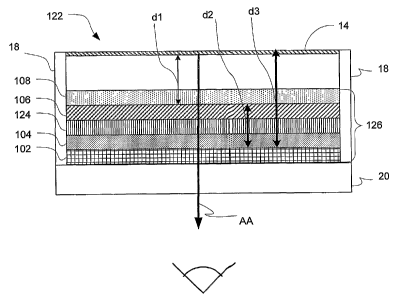
Figure 11 is a side cross-sectional view of an exemplary interferometric
modulator
122 that includes a wavelength filter. In one embodiment, the modulator 122
includes the
thin film wavelength filter as part of an optical stack 126 forrned on the
substrate 20. The
optical stack 126 includes a partially reflective layer 102, a transparent
dielectric layer 104, a
transparent electrode 124, a partially reflective layer 106, and a dielectric
layer 108. The
optical stack 126 is positioned with respect to the reflective layer 14 so as
to define a cavity
region in which the reflective layer 14 may move upon deflection. In one
embodiment, the
reflective layer 14 is connected to the substrate 20 by the posts 18.
Generally, the modulator
122 may include features according to any embodiment of the modulator 12
disclosed herein.
The dielectric layer 104 and partially reflective layers 102 and 106 together
define an
optical cavity that form an interferometric wavelength filter. As discussed
above, the
thiclcness and composition (index of refraction) of the dielectric layer 104
can be adjusted to
vaiy the effective optical path length of the optical cavity forrned between
layers 102 and 106
to produce the desired color filter. For example, the dielectric rnaterial may
be selected such
that a magenta filter is produced. If the interferometric device is set up to
produce green light
(in the absence of a wavelength filter), the magenta filter will adjust the
wavelength of output
light such that it appears white to the viewer. In other embodiments, the
dielectric layer is
adjusted to form a red, green or blue band pass filters as desired. Such
filters only allow the
desired wavelength of light to pass into and out of the device. As noted witlz
reference to
Figures 8 and 9, such wavelength filters may employed to increase the
saturation of colored
light produced by the modulator 12 and tliereby increase the color gamut of a
display
including the modulator 12 comprising the optical stack 126.
-23-
CA 02580992 2007-03-21
WO 2006/036540 PCT/US2005/032633
For example, one embodiment includes modulators 122 in which the optical path
length, d, is selected to produce a first order green spectral response. The
optical stack 126 in
such modulators 122 is configured to increase the saturation of the green. FoT
example, the
reflective layer 102 may comprise a thin (30 angstroms rather than 50-80
angstroms) chrome
layer. In another similar embodiment, the optical stack 126 may be configured
to output
magenta light when illuminated with white light so that the modulator 122 so
construction
reflects white light.
The production of an interferometric modulator device incorporating a
wavelength
filter in the optical stack 126 requires only a few additional process steps
compared to the
production of an interferometric modulator device without the filter. In the
example
illustrated in Figure 11, incorporation of the wavelength filter requires only
the additional
steps of depositing the dielectric layer 104 and the partially reflective
layer 102. The
additional processing requirements can be further reduced or minimized if the
dielectric layer
104 comprises the same material as the dielectric layer 108 and/or if the
partially reflective
layer 102 is made of the same material as the partially reflective layer 106.
Without subscribing to any particular theory of operation, the reflective
layer 14 and
the reflective layer 106 defines a first optical cavity characterized by the
optical path, dl,
therebetween. The optical stack 126 defines a second optical cavity
characterized by an
optical path length d2 between the partially reflective layers 106 and 102. In
addition, the
reflective layer 14 and the partially reflectively 102 define a third cavity
having the optical
path length d3 therebetween. Thus, in some embodiments, the output of the
modulator 12
may be further adjusted by selection of the layers of the optical stack 126
and the optical path
lengths d3 so as to select visible light properties of this third cavity. In
other embodiments,
these parameters may be selected so that the third cavity does not provide any
significant
contribution to visible light spectral response of the modulator 12.
Generally, the color of light reflected by the interferometric modulator 122
shifts
when the modulator 122 is viewed from different angles. The color of light
reflected from
the interferometric modulator 122 may vary for different angles of incidence
(and reflection)
with respect to an axis AA as illustrated in Figure 11. With increasing view
angle, the
effective optical path of the interferometric modulator is decreased according
to the
-24-
CA 02580992 2007-03-21
WO 2006/036540 PCT/US2005/032633
relationship 2d cos P = NX, where (3 is the view angle (the angle between the
normal to the
display and the incident light). With increasing view angle, the peak resonant
wavelength of
the reflected light is decreased. The user therefore perceives different
colors depending on
his or her angle of view. As described above, this phenomenon is referred to
as a "color
shift." This color shift is typically identified with reference to a color
produced by an
interferometric modulator 12 when viewed along the axis AA. In one embodiment,
the
optical stack 126 is configured to selectively filter light that "shifted"
outside of the desired
range of colors for a particular modulator. Thus, rather than appearing to
change color as
view angle increases, such an interferometric modulator 122 tends to output
light of a
reduced intensity at increasing angles as the modulators output is shifted
outside of the range
of wavelengths transmitted by the wavelength filter. In one embodiment, an
absorptive filter
may be included in the optical stack 126 to filter such light. In another
embodiment, an
interference filter in the optical stack 126 may be configured to filter such
color shifted liglit.
The interference filter may also be subject to such color shift. However,
because the
dielectric layer 104 has, in one embodiment, an index of refiaction that is
larger than that of
air in the gap 18 (as shown in Figure 11), the color shift is still reduced as
compared to the
modulator 122. In particular, as light enters the higher index dielectric
layer, it is directed to
a more normal angle to the reflective layers thus affecting the optical path
within the
interference filter and thereby reducing color shift. For example, if the
modulator 122
reflects green light and the interference filter portion of the optical stack
transmits green light,
the range of green transmitted wavelengths shifts less than the shift in range
of green
reflected wavelengths fiom the modulator. The intensity of shifted light is
thereby reduced in
aggregate. The overall brightness of such a device is also reduced, reducing
the eye's
perception of any change in the hue of output light.
The interferometric modulator 122 can be used in many different embodiments of
a
display. For example, one embodiment includes the display array 30 comprising
interferometric modulators 122 in which the optical path length, d2, of the
stack 126 is
selected to adjust the color balance, or white point of the display array 30.
In one
embodiment, the reflective layers 14 and 106 and the dielectric layer 108 are
configured so
that in the actuated position, the reflective layer 14 comprises a broadband
(or white)
-25-
CA 02580992 2007-03-21
WO 2006/036540 PCT/US2005/032633
reflector). In such an embodiment, the layers of the optical stack 126 are
configured as a
color filter so that the modulator 122 outputs colored light. In one such
einbodiment, the
display 30 is a color display that includes a plurality of modulators 122 in
which the movable
reflective layer 14 is configured to be a broadband reflector. Such an
embodiment of the
color display 30 produces color by configuring the optical stack 126 in
different portions of
the display (e.g., different columns) to produce, for example, red, green, and
blue light from
the modulators 122. Such color displays 30 allow the movable reflector (MEMS)
portion of
the display for each color to be formed to be substantially identical with
only the optical stack
portion of the color modulators being varied. Alternatively, a similar
embodiment includes
modulators 122 in which the optical path length, dl, is selected to produce
multiple peaks in
the visible spectrum corresponding to primaly colors such as red, green, and
blue. The
optical stack 126 of such modulators may be configured so that portions of the
modulators
122 in a particular display 30 output each of the primary colors, e.g.,
columns of alternating
red, green, and blue modulators so as to produce a color display. Other
configurations are
possible. For example, the thickness of dielectric 104 may be varied to
produce different
colors. Thus, in one embodiment, different portions of a display configured to
display
different colors may not have a uniform structure. Thus in one embodiment that
includes red,
green, and blue pixels forming a color display, the light modulators for each
of the colors
may be arranged in rows or columns that each have a different stack structure.
While the above detailed description has shown, described, and pointed out
novel
features of the invention as applied to various embodiments, it will be
understood that
various omissions, substitutions, and changes in the form and details of the
device or process
illustrated may be made by those skilled in the art without departing from the
spirit of the
invention. For example, additional layers may be added, layers may be removed
or ordered
differently. Different geometries and materials may be used. Other variations
are possible as
well. As will be recognized, the present invention may be embodied within a
form that does
not provide all of the features and benefits set forth herein, as some
features may be used or
practiced separately from others. The scope of the invention is indicated by
the appended
claims ratlier than by the foregoing description. All changes which come
within the meaning
and range of equivalency of the claims are to be embraced within their scope.
-26-