Note: Descriptions are shown in the official language in which they were submitted.
CA 02581230 2007-03-21
WO 2006/033582 PCT/N02005/000348
APPARATUS FOR FINGERPRINT SENSING AND OTHER MEASUREMENTS
FIELD OF INVENTION
The invention primarily relates to a method and an
apparatus for measuring patterns in a partially heat
conducting surface, preferably a fingerprint. In its wider
aspects the invention makes possible measurements also of
other forms of patterns in or on a surface of various
types of objects.
DESCRIPTION OF THE PRIOR ART
A number of different techniques to fingerprint image
capturing have been described in the open literature.
Generally, the sensor signal domain can be optical,
electrical, pressure-related or thermal.
The older method based on ink and paper has proven to be
unpractical. Optical sensors are typically large and
bulky. A family of fingerprint recording devices makes use
of a sensor array combined with a read out integrated
circuit, both components being fabricated on the same
substrate. The parameters measured by the sensors vary
greatly. For example, various electrical properties
characterising the finger skin pattern have been used as
measuring parameters in different fingerprint sensing
systems. Ohmic resistance, capacitance, complex impedance
and electric fields have all been mentioned as possible
parameters in the description of such systems. These types
of sensors are subjected to potential damages from
electrostatic discharges upon finger touching, as sensing
electrodes are usually made opened and very close to the
sensor surface. Other systems are based on pressure
sensors (micro-switches, piezoelectric sensors, etc.).
These pressure sensor based systems often include
membranes or micro-membranes that must be very soft and at
the same time be able to withstand wear, scratches and
repeated deformations which can reduce the device
lifetime.
One category of fingerprint reading systems is based on
temperature sensor arrays. In this particular case, the
equilibrium temperature of each sensor is a function of
the thermal contact between the finger and the sensor. A
good thermal contact, corresponding to fingerprint ridges,
will typically induce a larger sensor temperature change
than a bad thermal contact. The sensors for which the
temperature remains unaffected by the finger contact, at
least for some amount of time, correspond to fingerprint
valleys. The problem with this approach is that any
CA 02581230 2007-03-21
WO 2006/033582 PCT/N02005/000348
2
available temperature differentials will quickly fade away
when the system naturally reaches a state of thermal
equilibrium in a very short time. A quick sweeping of the
fingerprint across a line sensor may capture the initial
temperature differentials. However, this method requires
more elaborated data processing algorithms to retrieve the
full fingerprint representation. Moreover, it is much more
demanding on the sensor response time and on the system
data acquisition rate.
Since a fingerprint sensor may be exposed to long term use
in varying and sometimes demanding conditions the sensor
needs to have a robust surface, to be as insensitive to
contaminations in the fingerprint and on the sensor as
possible, and to be able to be screened electrically in
order to avoid interferences from outside and to protect
the sensor from electromagnetic discharges that can harm
the electronic circuits in the sensor. It must be capable
of reading most fingerprints without being severely
disturbed by latent prints from earlier use. It must also
be capable of reading worn fingerprints in which the
pattern is no longer visible. In some applications, such
as when integrated onto a contact /contact-less payment
chipcards /smartcards or electronic passports, a sensor
should be made very compact, physically.flexible
(bendable), and should have lowest possible power
consumption. In the view of costs there is also a demand
for simplicity and minimizing of the number of parts.
The thermal sensor principle, as described in the U.S.
Pat. No. 6,091,837, can satisfy the above-mentioned
requirements. It makes use of heat transfer mechanism in
order to distinguish fingerprint valleys and ridges, as
their skin structures have different heat transfer
characteristics. For this type of system, a sensor array
is heated and the heat exchange between the finger and the
underlying individual sensors is monitored through a
sensor temperature variation measurement. A relative large
sensor temperature indicates an accumulation of heat
energy, in other words, a little heat loss or a small heat
exchange between the considered sensor and the finger at
this point. Small heat exchanges, in turn, correspond to
low thermal conductivity (i.e. having low heat conduction
/transfer) points for which the thermal contact between
the finger and the sensor is very poor. Following this
approach, the low thermal conductivity points map the
local fingerprint valleys structure, and the high thermal
conductivity (i.e. having high heat conduction /transfer)
points map the local fingerprint ridges structure, and
intermediate thermal conductivity points correspond to the
local transition zone between ridges and valleys.
CA 02581230 2007-03-21
WO 2006/033582 PCT/N02005/000348
3
One implementation of this thermal principle is described
more closely in the international application no. WO
03098535. In this patent publication, separate resistors
are used as heater and temperature sensing element. An
array network of these resistors is deposited on a
flexible substrate. A pixel consists of a resistive heater
and a resistive temperature sensing element. Column and
row lines are routed and connected directly to an external
integrated circuit (ASIC) which contains all necessary
electronic switches, operational amplifiers and processing
circuitry. In operation, pixels are heated by the
resistive heaters and pixel temperatures are monitored by
the resistive sensing elements. Row and line switching is
done on the ASIC. All pixels belonging to a sensor column
are heated and processed at once, each column in turn. One
end of the resistive sensing elements are connected to
sensor rows and to be kept at a virtual potential
reference by the operational amplifiers.
One major drawback of this implementation is that all
pixels on a column are heated at the same time. This will
result in a high power consumption, especially for larger
sensor arrays with a high number of column pixels, assumed
a given signal/noise ratio has to be maintained. Another
potential issue is the varying resistive losses in upper
column line paths when these carry large heating currents.
This can result in inaccuracies and mismatches in pixel
heating power and/or pixel signals (due to varying line
voltage drops), and the larger array the worse.
Compensations may be done to overcome this problem, for
example by varying line widths to achieve identical line
losses in column line paths, but this approach could not
be done without a layout penalty. Inaccuracies and
mismatches may also be compensated and corrected by image
processing software, however, this adds complexity and
requires more computing resources, especially for sensors
used in portable embedded systems.
The present invention is a result of further development
to the sensor principle described in the U.S. Pat. No.
6,091,837. An objective of the invention is to able to
make the sensor physically compact and flexible, and with
low enough power consumption in order to be used for
example in wireless applications, such as in contact-less
chipcards /smartcards. Another objective is to be able to
implement a sensor being simple and cheap in production,
and robust in long-term use.
SUMMARY OF THE INVENTION
On the above background this invention is generally
directed to an apparatus for measuring a pattern in a
surface of an object and comprising a plurality of sensor
CA 02581230 2007-03-21
WO 2006/033582 PCT/N02005/000348
4
elements being responsive to a physical parameter of the
object surface, as well as means for establishing an
overall, segmented picture related to said pattern. The
novel and specific features according to the invention
primarily consist therein that the apparatus comprises at
least one diode functionally associated with each sensor
element for contributing to one or more of the following
functions:
- selectively addressing said sensor element
- activating said sensor element, and
- sensing of said physical parameter.
In the very interesting case of an object being at least
partially heat conducting, in particular a fingerprint,
the above at least one diode is adapted to be activated by
being heated with an applied electric current, and/or the
diode is comprised by the associated sensor element and is
adapted to sense the temperature at the sensor element.
Other novel and specific features according to this
invention are expressed in the attached claims.
The solution is presented in the following sections. In
short, a simple sensor element or pixel structure is made
and there is no active transistor inside the pixel
elements. In spite of this, sensor pixels can still be
addressed individually. Power consumption is kept at a low
level, since only one or a very limited number of pixels
are addressed and heated at a time. Practical problems
with resistive column/row line losses can be eliminated,
firstly by carrying low heating currents, and secondly by
using current source(s) while detecting pixel thermal
changes upon a heat excitation. Physical flexibility is
achieved by using a flexible substrate. Further, sensor
production costs can be minimized by preferably splitting
the sensor in two main parts: a pixel array (large area)
and a processing chip (small area). The pixel array can
preferably be produced using large-area or roll-to-roll
processing techniques, while the processing chip can be
produced in semiconductor standard processes. The pixel
array and the processing chip are then connected together
by using conventional bonding techniques or flip-chip
technology.
BRIEF DESCRIPTION OF THE DRAWINGS
In the following description embodiments of the invention
will be explained more in detail with reference to figures
of drawings:
Fig. 1 in simplified form shows a single sensor element or
CA 02581230 2007-03-21
WO 2006/033582 PCT/N02005/000348
pixel with a number of diodes as functional components,
Fig. 2 in schematic cross-section shows an example of a
possible type of diode that may be useful in the sensor
elements,
Fig. 3 in schematic cross-section shows an example of a
possible "vertical" sensor element structure,
Fig. 4 shows an embodiment of a circuit configuration for
a sensor array of relatively limited size,
Fig. 5 shows another circuit configuration suitable for a
larger array size than the one in Fig. 4,
Fig. 6 in plan view and elevation, respectively, shows a
practical arrangement of a sensor apparatus main parts
Fig. 7 in a corresponding way as Fig..1 shows a single
pixel, but with a generic form of sensor element.
DETAILED DESCRIPTION OF THE DRAWINGS
Reference is made to Fig. 1.
In a sensor element or pixel 4, one or more diodes D1-Dn
are connected in series between pixel row line 2 and pixel
column line 3, as illustrated in figure 1. The diodes D1-
Dri should be close to the sensor surface and in good
thermal contact with a fingerprint to be measured.
These pixel diodes D1-Dn in this embodiment will act both
as pixel heater and temperature sensing element.
Furthermore, as diode is a rectifier and when connected as
illustrated and correctly biased, they will enable a
simple pixel addressing, i.e. selecting /processing some
pixel(s) of interest while deselecting /isolating all
other pixels in the sensor array. Pixel addressing is done
by controlling the potentials of pixel rows 2 and columns
3, in such a way that the selected pixel diodes D1-Dn are
correctly biased (the current flows only through the
selected pixel diode(s), while other pixels in the array
are open-circuited /blocked). Thus, in this case the
diodes or possibly one diode only, will perform all the
functions of addressing, activating and sensing, as
mentioned above.
The pixel is heated when these diodes D1-Dn are forward-
biased with a given current ID and voltage VD across each
diode. As diode is usually a temperature-sensitive device,
any temperature change in a pixel will reflect a
corresponding voltage change AVD across each diode.
Pixel heating power and thermal signal can be defined as
followed:
Pixel heating power: n=VD=In
Thermal voltage signal: n=AVD (for a given constant
diode current ID)
CA 02581230 2007-03-21
WO 2006/033582 PCT/N02005/000348
6
where n _l is the number of pixel diodes connected in
series. The number n is mainly limited by practical pixel
circuit layout and fabrication, and by the diode's barrier
height and the operating voltage of a sensor system.
The amount of voltage change AVD in a pixel diode, upon
heat excitation, will depend on local heat transfer with a
fingerprint which is applied on the sensor surface. Ridge
regions with better heat conduction (yielding larger heat
loss) will normally have smaller voltage change AVD than
valley regions with poorer heat conduction (yielding
smaller heat loss).
Alternatively, pixel diode can be kept at a constant bias
voltage VD. Any temperature change in a pixel will then
reflect a correspondent current change AIp through the
diode(s). In this case, the parameter AID is used as pixel
thermal signal.
A fingerprint image pattern is built by addressing,
heating and collecting all pixel thermal signals in the
sensor array. Differentials in either AVD or AID will
distinguish valleys and ridges, thus representing a
fingerprint image. The diode(s) may be adapted to sense
the temperature at each sensor element or pixel either
intermittently or continuously.
There are several ways to construct a rectifier/diode in
microelectronics. There also exist different diode types
with their own characteristics suitable for different
applications. The pixel diode(s) in this application'can
be any microelectronic device construction, with either
purely or combined rectifying characteristic. The diode
may preferably be, but not limited to, a PN-junction
rectifier, a Schottky rectifier, or a PIN diode.
The diodes D1-Dn may be constructed from selected
compound-semiconductor or semiconductor materials
(preferably, but not limited to, Germanium or Silicon) and
metal (for example aluminum, in case of some Schottky
diodes) with suitable properties, or completely from
organic materials. The atomic structures may be mono-
crystalline, amorphous or poly-crystalline.
For illustration purpose, Figure 2 shows an example of a
lateral /planar Schottky rectifier, which is formed in the
contact interface 43 between a semiconductor 42 (for
example N-type Silicon) and a suitable metal 44 (for
example aluminum). Metal contacts 40 and 44 are the diode
CA 02581230 2007-03-21
WO 2006/033582 PCT/N02005/000348
7
terminals. The N-F islands 41 ensure that the contacts at
the terminals 40 are ohmic contacts. An insulating oxide
46 may surround the diode device structure.
Figure 3 is an example of the vertical structure of the
sensor, drawn (not to scale) with a single diode D1 and
with a fingerprint F with surface A applied on the sensor.
The substrate 45 can be rigid or preferably physically
flexible. Substrate materials can be a plastic (for
example PET, PEN...), a metal foil (for example steel,
aluminum...) or semiconductor (for example silicon...) ,
quartz, glass or any material that is suitable for
depositing microelectronic structures in production.
The insulator 46 may be an oxide from metal or
semiconductor, or an organic material. Row 2 and column 3
connections can be made from a suitable metal (for example
aluminum).
The sensor pixels are covered with a conductive /semi-
conductive layer 47 which should be grounded to shield the
sensor electrically, and to protect the sensor from
potentially harmful electromagnetic discharges upon
accidental finger touching. A robust coating 48 on top can
provide the mechanical and chemical protection in daily
uses.
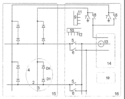
Figure 4 is a simplified diagram of a sensor system that
preferably consists of two main parts: a pixel array 15
and a processing chip 16. Nevertheless, these two parts
may also be integrated on a single common substrate.
The pixel array 15 is a two-dimensional network of pixels
4 with one or more diodes D1-Dn connected in series inside
each pixel. Pixels 4 are connected to the global row 2 and
column lines 3. Row 2 and column lines 3 are then routed
and connected externally to the processing chip 16.
In the processing chip 16, there are switches for rows and
columns. The column switches 7 and 8 are controlled by the
outputs 11 of a column line selector 9 which may
preferably be a shift register or a decoder logic. In the
same way, the row switches 5 and 6 are controlled by the
outputs 12 of a row line selector 10 which may preferably
be a shift register or a decoder logic. For each column 3
and each row 2, there are preferably a main switch and a
signal switch. The main switches 5 and 7 can handle large
currents, while corresponding signal switches 6 and 8 will
pass the sensor signals to an internal analogue circuit
CA 02581230 2007-03-21
WO 2006/033582 PCT/N02005/000348
8
14. The use of signal switches 6 and 8 can minimize the
effects of noise and other irregularities in the main
switches 5 and 7. For this purpose the signal switches are
connected to the sensor pixel elements 4 at points between
the sensor elements and respective main switches.
The switches 5, 6, 7 and 8 may be of any microelectronic
devices that can perform the switching or equivalent
functions. Additional circuit control may be needed to
ensure a proper biasing and addressing of pixel diodes Dl-
Dn.
Current from a current source 13 is fed to the pixel being
addressed. The current source 13 can be dynamically
controlled and adjustable. Any changes in the selected
pixel's thermal signal is monitored and processed by the
internal analogue circuit 14, based on heat activation of
one sensor pixel element at a time. In some instances it
may be preferred to use a constant current source 13.
The processing chip 16 may also contain other circuit
blocks 19 as well, for example the necessary electronics
to perform complex fingerprint image processing,
registration, fingerprint matching, and access control to
applications. Anyhow, chip 16 in this embodiment provides
means for establishing an overall, segmented picture
related to the surface pattern to be measured, in
particular a fingerprint.
This circuit configuration, as shown in figure 4, may be
suitable for a sensor with a limited pixel array size. For
a large pixel array, the high number of row 2 and column
lines 3 to be connected externally will require many
bonding pads and excessive contact areas, making the total
sensor size impractical large (pixel array 15, processing
chip 16 or both) for some applications.
The circuit configuration of figure 5 is similar to figure
4, except that the row and column switching functions are
totally incorporated in a now highly-integrated pixel
array 17. The number of external connections to a now
simpler processing chip 18 is then dramatically reduced to
a few lines.
This configuration is preferred for larger sensor array
size.
The switches and row /column line selectors may be
constructed from thin-film transistors (TFTs) or
semiconductor devices capable of performing the equivalent
CA 02581230 2007-03-21
WO 2006/033582 PCT/N02005/000348
9
functions.
In order to maximize the array scanning speed in for
example very large pixel arrays, several or a small group
of pixels 4 may preferably be selected and processed at a
time. In such cases, the sensor may be split into
subsections for parallel processing.
Figure 6 is a top and side view of the sensor system.
The pixel array 15 (17) is made on a (flexible) substrate
45. The processing chip 16 (18) is bonded on the array
substrate 45. Vertical 22 and horizontal connections 21
are routed and connected between these two parts.
In/Out lines 20 may be made available to be physically
connected to an external system.
In the pixel circuit 71 in Fig. 7, there is a generic
sensing element, here drawn in the form of a resistor 73,
and a diode 75 connected in series between row 2 and
column lines 3. Element 73 in addition to - or instead of
- the sensing function, can contribute substantially to
the required heating.
The diode 75 can be used purely for pixel addressing, as
it will, when correctly biased, permit current flow in one
direction while blocking current in the opposite
direction. It can also be used partly as a sensing element
together with the generic sensing element 73. This will
depend on pixel structures, designs and applications.
The generic sensing element 73 can comprise a passive
device (such as a resistor, capacitor, inductor ...) or any
other type of devices of interest (such as a membrane
switch, an active transistor /device ...).
For pixel heating and temperature sensing purposes in the
current application (i.e. fingerprint image capturing),
the diode 75 may preferably be used for pixel addressing
purpose only. Under control by circuits 14, 16, 18 (Figs.
4 and 5) there may be provided for selective addressing of
one sensor pixel element or a small group of sensor
elements at a time, by means of an array of diodes 75. In
a practical apparatus a small group may range from 2-4 to
more sensor elements, depending on possible subdivision of
a large sensor array, time allotted for each overall
I segmented picture, required resolution, thermal_parameters
and so forth.
The generic sensing element 73 may preferably be a
CA 02581230 2007-03-21
WO 2006/033582 PCT/N02005/000348
resistive material to be used as a combined heating and
temperature-sensitive resistor. Such resistor device
should be made very close to the sensor surface in order
to interact thermally with an applied fingerprint. When
heated with a current flow, the resistive value will
partly change according to the heat transfer with the
fingerprint on the sensor surface. The change in resistive
value is monitored and used as a measure for pixel thermal
signal.
The rest of the sensor system or apparatus will remain the
same as described in earlier sections above.
A diode structure is basically sensitive to temperatures
and exposed lights, and a resistor material can be made to
have an optimal response to temperatures, lights, or
pressure. Thus, the ideas and basic structures of the
present pixel and sensor system can also be further used
to create an image or to perform other types of
measurements based on light intensity, pressure and
temperatures.
These types of measurements can also be of interest for
fingerprint sensing.
However, as will be understood from the above description,
the primary aspect of this invention is related to
fingerprint sensing based on pixel thermal signal.