Note: Descriptions are shown in the official language in which they were submitted.
CA 02581248 2007-03-21
WO 2006/137876 PCT/US2005/033718
Random Access Memory Including Nanotube Switching Elements
Cross-Reference to Related Applications
[0001] This application claims priority under 35 U.S.C. 119(e) to U.S.
Provisional
Pat. Apl. No. 60/612,300, filed on September 22, 2004, entitled Random Access
Menaory Including Nanotube Switching Elements, which is incorporated herein by
reference in its entirety.
[0002] This application is a continuation-in-part and claims priority under 35
U.S.C.
120 to U.S. Pat. Apl. No. 10/918,085, filed on August 13, 2004, entitled
Nanotube-
Based Switching Elements with Multiple Controls, and hereby incorporates such
reference in its entirety.
Background
1. Technical Field
[0003] The present application generally relates to nanotube switching
circuits
and in particular to nanotube switching circuits that can be used to provide
non-
volatile storage functionality to otherwise conventional random access memory
(RAM).
2. Discussion of Related Art
[0004] Digital logic circuits are used in personal computers, portable
electronic
devices such as personal organizers and calculators, electronic entertainment
devices,
and in control circuits for appliances, telephone switching systems,
automobiles, aircraft
and other items of manufacture. Early digital logic was constructed out of
discrete
switching elements composed of individual bipolar transistors. With the
invention of
the bipolar integrated circuit, large numbers of individual switching elements
could be
combined on a single silicon substrate to create complete digital logic
circuits such as
inverters, NAND gates, NOR gates, flip-flops, adders, etc. However, the
density of
bipolar digital integrated circuits is limited by their high power consumption
and the
ability of packaging technology to dissipate the heat produced while the
circuits are
operating. The availability of metal oxide semiconductor ("MOS") integrated
circuits
CA 02581248 2007-03-21
WO 2006/137876 PCT/US2005/033718
using field effect transistor ("FET") switching elements significantly reduces
the power
consumption of digital logic and enables the construction of the high density,
complex
digital circuits used in current technology. The density and operating speed
of MOS
digital circuits are still limited by the need to dissipate the heat produced
when the
device is operating.
[0005] Digital logic integrated circuits constructed from bipolar or MOS
devices
do not function correctly under conditions of high heat or extreme
environments.
Current digital integrated circuits are normally designed to operate at
temperatures
less than 100 degrees centigrade and few operate at temperatures over 200
degrees
centigrade. In conventional integrated circuits, the leakage current of the
individual
switching elements in the "off ' state increases rapidly with temperature. As
leakage
current increases, the operating temperature of the device rises, the power
consumed
by the circuit increases, and the difficulty of discriminating the off state
from the on
state reduces circuit reliability. Conventional digital logic circuits also
short
internally when subjected to certain extreme environments because electrical
currents
are generated inside the semiconductor material. It is possible to manufacture
integrated circuits with special devices and isolation techniques so that they
remain
operational when exposed to such environments, but the high cost of these
devices
limits their availability and practicality. In addition, such digital circuits
exhibit
timing differences from their normal counterparts, requiring additional design
verification to add protection to an existing design.
[0006] Integrated circuits constructed from either bipolar or FET switching
elements are volatile. They only maintain their internal logical state while
power is
applied to the device. When power is removed, the internal state is lost
unless some
type of non-volatile memory circuit, such as EEPROM (electrically erasable
programmable read-only memory), is added internal or external to the device to
maintain the logical state. Even if non-volatile memory is utilized to
maintain the
logical state, additional circuitry is necessary to transfer the digital logic
state to the
memory before power is lost, and to restore the state of the individual logic
circuits
when power is restored to the device. Alternative solutions to avoid losing
information in volatile digital circuits, such as battery backup, also add
cost and
complexity to digital designs.
2
CA 02581248 2007-03-21
WO 2006/137876 PCT/US2005/033718
[0007] Important characteristics for logic circuits in an electronic device
are low
cost, high density, low power, and high speed. Conventional logic solutions
are
limited to silicon substrates, but logic circuits built on other substrates
would allow
logic devices to be integrated directly into many manufactured products in a
single
step, further reducing cost.
[0008] Devices have been proposed which use nanoscopic wires, such as single-
walled carbon nanotubes, to form crossbar junctions to serve as memory cells.
See
WO 01/03208, Nanoscopic Wire-Based Devices, Arrays, and Methods of Their
Manufacture; and Thomas Rueckes et al., "Carbon Nanotube-Based Nonvolatile
Random Access Memory for Molecular Computing," Science, vol. 289, pp. 94-97, 7
July, 2000.) Hereinafter these devices are called nanotube wire crossbar
memories
(NTWCMs). Under these proposals, individual single-walled nanotube wires
suspended over other wires define memory cells. Electrical signals are written
to one
or both wires to cause them to physically attract or repel relative to one
another. Each
physical state (i.e., attracted or repelled wires) corresponds to an
electrical state.
Repelled wires are an open circuit junction. Attracted wires are a closed
state forming
a rectified junction. When electrical power is removed from the junction, the
wires
retain their physical (and thus electrical) state thereby forming a non-
volatile memory
cell.
[0009] U.S. Patent Publication No. 2003-0021966 discloses, among other things,
electromechanical circuits, such as memory cells, in which circuits include a
structure
having electrically conductive traces and supports extending from a surface of
a
substrate. Nanotube ribbons that can electromechanically deform, or switch are
suspended by the supports that cross the electrically conductive traces. Each
ribbon
comprises one or more nanotubes. The ribbons are typically formed from
selectively
removing material from a layer or matted fabric of nanotubes.
[0010] For example, as disclosed in U.S. Patent Publication No. 2003-0021966,
a
nanofabric may be patterned into ribbons, and the ribbons can be used as a
component
to create non-volatile electromechanical memory cells. The ribbon is
electromechanically-deflectable in response to electrical stimulus of control
traces
and/or the ribbon. The deflected, physical state of the ribbon may be made to
3
CA 02581248 2007-03-21
WO 2006/137876 PCT/US2005/033718
represent a corresponding information state. The deflected, physical state has
non-
volatile properties, meaning the ribbon retains its physical (and therefore
informational) state even if power to the memory cell is removed. As explained
in
U.S. Patent Publication No. 2003-0124325, three-trace architectures may be
used for
electromechanical memory cells, in which the two of the traces are electrodes
to
control the deflection of the ribbon.
[0011] The use of an electromechanical bi-stable device for digital
information
storage has also been suggested (c.f. US4979149: Non-volatile memory device
including a micro-mechanical storage element).
[0012] The creation and operation of bi-stable, nano-electro-mechanical
switches
based on carbon nanotubes (including mono-layers constructed thereof) and
metal
electrodes has been detailed in a previous patent application of Nantero, Inc.
(U.S.
Patent Nos. 6574130, 6643165, 6706402, 6784028, 6835591, 6911682, 6919592, and
6924538; and U.S. Patent Apl. Nos. 10/341005, 10/341055, 10/341054, 10/341130,
and 10/776059, the contents of which are hereby incorporated by reference in
their
entireties).
Sumfnary
[0013] The present invention provides random access memory including nanotube
switching elements.
[0014] Under one aspect of the invention a memory cell includes first and
second
nanotube switching elements and an electronic memory. Each nanotube switching
element includes an output node, a nanotube channel element having at least
one
electrically conductive nanotube, and a control structure having a set
electrode and a
release electrode disposed in relation to the nanotube channel element to
controllably
form and unform an electrically conductive channel between said channel
electrode
and said output node. The electronic memory has cross-coupled first and second
inverters. The input node of the first inverter is coupled to the set
electrode of the first
nanotube switching element and to the output node of the second nanotube
switching
element. The input node of the of the second inverter is coupled to the set
electrode
4
CA 02581248 2007-03-21
WO 2006/137876 PCT/US2005/033718
of the second nanotube switching element and to the output node of the first
nanotube
switching element; and the channel electrode is coupled to a channel voltage
line.
[0015] Under another aspect of the invention, the release electrode of the
first
nanotube switching element is coupled to the release electrode of the second
nanotube
switching element and wherein both release electrodes are coupled to a release
line.
[0016] Under another aspect of the invention, the first and second inverters
are
CMOS inverters.
[0017] Under another aspect of the invention, the first and second nanotube
switching elements are non-volatile state devices.
[0018] Under another aspect of the invention, the first and second nanotube
switching elements are fabricated in circuit layers above circuit layers used
to
fabricate the electronic memory.
[0019] Under another aspect of the invention, the channel voltage line is set
to
one-half the supply voltage used by the electronic memory, when the circuit
operates
in an electronic memory mode. The channel voltage line is set to nanotube
channel
switching voltage, when the circuit operates in a shadow memory mode. In
shadow
memory mode, the state of the electronic memory transfers to the state of the
nanotube switching elements.
[0020] Under another aspect of the invention, the channel voltage line is set
to the
supply voltage used by the electronic memory, when the circuit operates in a
recall
mode. In the recall mode the state of the nanotube switching elements
transfers to the
state of the electronic memory.
[0021] Under another aspect of the invention, the release electrode of the
first
nanotube switching element is coupled to the release electrode of the second
nanotube
switching element and both are coupled to a release line. After the recall
mode
transfers the state of the nanotube switching elements to the state of the
electronic
memory, the release line is activated to reset the state of the nanotube
switching
elements.
CA 02581248 2007-03-21
WO 2006/137876 PCT/US2005/033718
Brief Description of the Drawings
[0022] In the Drawing,
Figures 1A -1D illustrate cross-sectional views and a plan view of a nanotube
switching element of certain embodiments in two different states and include a
plan
view of such element;
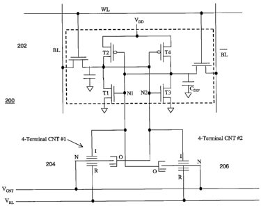
Figure 2 is a schematic view of a non-volatile random access storage element
in accordance with certain embodiments of the invention.
Detailed Description
[0023] Preferred embodiments of the invention provide switching elements in
which a nanotube-based switching element is included with an otherwise
conventional
RAM cell. The nanotube switching element may then be used to provide non-
volatile
storage functionality, for example, to act as a shadow ram. Moreover, the
design of
preferred embodiments of the nanotube switching elements may be included as
extra
layers on top of already formed RAM cells.
[0024] First, the nanotube switching element will be described. Second, the
integration of such an element with a RAM cell will be explained.
Nanotube Switching Element
[0025] Figure 1A is a cross sectional view of a preferred nanotube switching
element 100. Nanotube switching element includes a lower portion having an
insulating layer 117, control electrode 111, output electrodes 113c,d.
Nanotube
switching element further includes an upper portion having release electrode
112,
opposing output electrodes 113a,b, and signal electrodes 114a,b. A nanotube
channel
element 115 is positioned between and held by the upper and lower portions.
[0026] Release electrode 112 is made of conductive material and is separated
from nanotube channel element 115 by an insulating material 119. The channel
element 115 is separated from the facing surface of insulator 119 by a gap
height
G102.
6
CA 02581248 2007-03-21
WO 2006/137876 PCT/US2005/033718
[0027] Opposing output electrodes 113a,b are made of conductive material and
are separated from nanotube channel element 115 by insulating material 119.
[0028] Output electrodes 113c,d are likewise made of conductive material and
are
separated from nanotube channel element 115 by a gap height G103. Notice that
the
output electrodes 113c,d are not covered by insulator.
[0029] Control electrode 111 is made of conductive material and is separated
from nanotube channel element 115 by an insulating layer (or film) 118. The
channel
element 115 is separated from the facing surface of insulator 118 by a gap
height
G104.
[0030] Signal electrodes 1 14a,b each contact the nanotube channel element 115
and can therefore supply whatever signal is on the signal electrode to the
channel
element 115. This signal may be a fixed reference signal (e.g., VDD or Ground)
or
varying (e.g., a Boolean discrete value signal that can change). Only one of
the
electrodes 1 14a,b need be connected, but both may be used to reduce effective
resistance.
[0031] Nanotube channel element 115 is a lithographically-defined article made
from a porous fabric of nanotubes (more below). It is electrically connected
to signal
electrodes 1 14a,b. The electrodes 1 14a,b and support 116 pinch or hold or
pin the
channel element 115 at either end, and it is suspended in the middle in spaced
relation
to the output electrodes 113a-d and the control electrode 111 and release
electrode
112. The spaced relationship is defined by the gap heights G102-G104
identified
above. For certain embodiments, the length of the suspended portion of channel
element 115 is about 300 to 350 nm.
[0032] Under certain embodiments the gaps G103, G104, G102 are in the range of
5- 30 nm. The dielectric on terminals 112, 111, and 113a and 113b are in the
range
of 5- 30 nm, for example. The carbon nanotube fabric density is approximately
10
nanotubes per 0.2 x 0.2 um area, for example. The suspended length of the
nanotube
channel element is in the range of 300 to 350 nm, for example. The suspended
length
to gap ratio is about 5 to 15 to 1 for non-volatile devices, and less than 5
for volatile
operation, for example.
7
CA 02581248 2007-03-21
WO 2006/137876 PCT/US2005/033718
[0033] Figure lB is a plan view or layout of nanotube switching element 100.
As
shown in this figure, electrodes 113b,d are electrically connected as depicted
by the
notation 'X' and item 102. Likewise opposing output electrodes 11 3a,c are
connected
as depicted by the 'X'. In preferred embodiments the electrodes are further
connected
by connection 120. All of the output electrodes collectively form an output
node 113
of the switching element 100.
[0034] Under preferred embodiments, the nanotube switching element 100 of
figures 1A and 1B operates as shown in figures 1C and D. Specifically,
nanotube
switching element 100 is in an OPEN (OFF) state when nanotube channel element
is
in position 122 of figure 1C. In such state, the channel element 115 is drawn
into
mechanical contact with dielectric layer 119 via electrostatic forces created
by the
potential difference between electrode 112 and channel element 115. Opposing
output electrodes 113a,b are in mechanical contact (but not electrical
contact) with
channel element 115. Nanotube switching element 100 is in a CLOSED (ON) state
when channel element 115 is elongated to position 124 as illustrated in figure
1D. In
such state, the channel element 115 is drawn into mechanical contact with
dielectric
layer 118 via electrostatic forces created by the potential difference between
electrode
111 and channel element 115. Output electrodes 113c,d are in mechanical
contact
and electrical contact with channel element 115 at regions 126. Consequently,
when
channel element 115 is in position 124, signal electrodes 1 14a and 114b are
electrically connected with output terminals 11 3c,d via channel element 115,
and the
signal on electrodes 114 a,b may be transferred via the channel (including
channel
element 115) to the output electrodes 113c,d.
[0035] By properly tailoring the geometry of nanotube switching element 100,
the
nanotube switching element 100 may be made to behave as a non-volatile or a
volatile
switching element. By way of example, the device state of figure 1D may be
made to
be non-volatile by proper selection of the length of the channel element
relative to the
gap G104. (The length and gap are two parameters in the restoring force of the
elongated, deflected channel element 115.) Length to gap ratios of greater
than 5 and
less than 15 are preferred for non-volatile device; length to gap ratios of
less than 5
are preferred for volatile devices.
8
CA 02581248 2007-03-21
WO 2006/137876 PCT/US2005/033718
[0036] The nanotube switching element 100 operates in the following way. If
signal electrode 114 and control electrode 111 (or 112) have a potential
difference that
is sufficiently large (via respective signals on the electrodes), the
relationship of signals
will create an electrostatic force that is sufficiently large to cause the
suspended,
nanotube channel element 115 to deflect into mechanical contact with electrode
111 (or
112). (This aspect of operation is described in the incorporated patent
references.) This
deflection is depicted in figure 1D (and 1C). The attractive force stretches
and deflects
the nanotube fabric of channel element 115 until it contacts the insulated
region 118 of
the electrode 111. The nanotube channel element is thereby strained, and there
is a
restoring tensil force, dependent on the geometrical relationship of the
circuit, among
other things.
[0037] By using appropriate geometries of components, the switching element
100
then attains the closed, conductive state of figure 1D in which the nanotube
channel 115
mechanically contacts the control electrode 111 and also output electrode 1
13c,d. Since
the control electrode 111 is covered with insulator 118 any signal on
electrode 114 is
transferred from the electrode 114 to the output electrode 113 via the
nanotube channel
element 115. The signal on electrode 114 may be a varying signal, a fixed
signal, a
reference signal, a power supply line, or ground line. The channel formation
is
controlled via the signal applied to the electrode 111 (or 112). Specifically
the signal
applied to control electrode 111 needs to be sufficiently different in
relation to the
signal on electrode 114 to create the electrostatic force to deflect the
nanotube channel
element to cause the channel element 115 to deflect and to form the channel
between
electrode 114 and output electrode 113, such that switching element 100 is in
the
CLOSED (ON) state.
[0038] In contrast, if the relationship of signals on the electrode 114 and
control
electrode 111 is insufficiently different, then the nanotube channel element
115 is not
deflected and no conductive channel is formed to the output electrode 113.
Instead, the
channel element 115 is attracted to and physically contacts the insulation
layer on
release electrode 112. This OPEN (OFF) state is shown in figure 1C. The
nanotube
channel element 115 has the signal from electrode 114 but this signal is not
transferred
to the output node 113. Instead, the state of the output node 113 depends on
whatever
circuitry it is connected to and the state of such circuitry. The state of
output node 113
9
CA 02581248 2007-03-21
WO 2006/137876 PCT/US2005/033718
in this regard is independent of channel element voltage from signal electrode
114 and
nanotube channel element 115 when the switching element 100 is in the OPEN
(OFF)
state.
[0039] If the voltage difference between the control electrode 111 (or 112)
and the
channel element 115 is removed, the channel element 115 returns to the non-
elongated
state (see figure 1 A) if the switching element 100 is designed to operate in
the volatile
mode, and the electrical connection or path between the electrode 115 to the
output
node 113 is opened.
[0040] Preferably, if the switching element 100 is designed to operate in the
non-
volatile mode, the channel element is not operated in a manner to attain the
state of
figure 1A. Instead, the electrodes 111 and 112 are expected to be operated so
that the
channel element 115 will either be in the state of Figure 1C or 1D.
[0041] The output node 113 is constructed to include an isolation structure in
which
the operation of the channel element 115 and thereby the formation of the
channel is
invariant to the state of the output node 113. Since in the preferred
embodiment the
channel element is electromechanically deflectable in response to
electrostatically
attractive forces, a floating output node 113 in principle could have any
potential.
Consequently, the potential on an output node may be sufficiently different in
relation
to the state of the channel element 115 that it would cause deflection of the
channel
element 115 and disturb the operation of the switching element 100 and its
channel
formation; that is, the channel formation would depend on the state of an
unknown
floating node. In the preferred embodiment this problem is addressed with an
output
node that includes an isolation structure to prevent such disturbances from
being
caused.
[0042] Specifically, the nanotube channel element 115 is disposed between two
oppositely disposed electrodes 113b,d (and also 113 a,c) of equal potential.
Consequently, there are equal but opposing electrostatic forces that result
from the
voltage on the output node. Because of the equal and opposing electrostatic
forces, the
state of output node 113 cannot cause the nanotube channel element 115 to
deflect
regardless of the voltages on output node 113 and nanotube channel element
115. Thus,
CA 02581248 2007-03-21
WO 2006/137876 PCT/US2005/033718
the operation and formation of the channel is made invariant to the state of
the output
node.
[0043] The nanotube switching element described above, along with various
alternatives to such, is explained in greater detail in U.S. Pat. Apl. No.
10/918,085, filed
on August 13, 2004, entitled Nanotube-Based Switching Elements with Multiple
Controls, which is hereby incorporated by reference in its entirety.
Ram with Nanotube Switching Element
[0044] In preferred versions, storage elements are constructed from
conventional
storage cell designs, for example using CMOS transistors, with additional
nanotube-
based non-volatile switching elements like those described above. In preferred
versions, the storage circuitry operates using non-volatile switching of
nanotubes.
[0045] However, 4-terminal device 100 is non-volatile and also includes a
release
node R. The outputs have opposing electrodes. The input electrode I has a
dielectric
layer over it so the CNT comes in physical but not electrical contact with the
input
electrode. The release electrode R has a dielectric layer under it so the CNT
comes in
physical but not electrical contact with the release electrode.
[0046] The 4-terminal non-volatile CNT device may be used as a shadow device,
for example, on each of the flip flop nodes of SRAM cells. These 4-terminal
devices
are added at or near the end of the process for an SRAM, and are used to store
information when power is lost or removed.
[0047] Figure 2 illustrates a memory cell 200 having a flip-flop based non-
volatile
RAM cell with an SRAM structure 202 and two CNT 4-terminal structures 204 and
206, one for each node N1 and N2 of the flip flop cell 202. See U.S. Pat. Apl.
No.
10/918,085, filed on August 13, 2004, entitled Nanotube-Based Switching
Elements
with Multiple Controls. This implementation offers various advantages
discussed above
because the CNTs can be added to an existing SRAM product and added to
existing
wafers. Operation is described below. The assumptions for this discussion of
the
operation of this implementation are as follows:
~ The CNT switching elements 204 and 206 are in a released state (CNT in
contact with the insulator of release plate R) during SRAM operation, prior to
the STORE operation
11
CA 02581248 2007-03-21
WO 2006/137876 PCTIUS2005/033718
= The CNT voltage VCNT applied to CNT channel element N is at VDD/2 so that
the FF 202 does not activate the CNTs prior to the STORE operation
The STORE operation for initially storing data in the cell, is as follows:
= STORE:
o SRAM operation is stopped
o The CNT voltage VCNT transitions from VDD/2 to Vsw, the voltage
required to switch the CNTs.
o CNT switching element activation takes place between the input I that
is held at ground by the flip flop and CNT channel element N which
transitions to VCNT = Vsw. The CNT switching element turns ON, and
voltage VCNT is applied to the output electrode of the CNT device by
contact with CNT channel element N. The output electrode is
connected to the opposite side of the flip flop which is positive.
o The CNT switching element with input voltage = 0 switches, the CNT
switching element output is positive, and therefore does not disturb the
flip flop state. The other CNT switching element remains in the
released (OFF) position
o Power supply VDD goes to zero
[0048] The nanotube switching elements retain the logic state of the flip flop
cell
especially if the storage element is powered down or if the power is
interrupted, for
example. The procedure for recalling stored data from a storage element is as
follows:
= RECALL:
o The CNT switching elements 204 and 206 are powered up. VCNT = VDD
o The SRAM is powered up to VDD
o Flip flops assume state corresponding to the logic state of the non-
volatile CNT switching elements.
o CNT switching elements are reset to the erase position (in contact with
oxide on release plate). This is accomplished by raising the release line
12
CA 02581248 2007-03-21
WO 2006/137876 PCT/US2005/033718
voltage VRL to high enough voltage to overcome electrostatic forces
between the input and the NT. This voltage may be greater than VDD.
o SRAM operation resumes
[0049] The inventors envision additional configurations of volatile and
nonvolatile
or mixed nanoelectromechanical designs depending upon the specific
application,
speed, power requirements and density desired. Additionally the inventors
foresee the
use of multiwalled carbon nanotubes or nanowires as the switching element of
contact
points within the switch. As the technology node decreases in size from 90 nm
to 65
nm and below down to the size of individual nanotubes or nanowires the
inventors
foresee adapting the basic electromechanical switching elements and their
operation to a
generation of nanoscale devices with scaleable performance characteristics
concomitant
with such size reduction.
[0050] The devices and articles shown in the preceding embodiments are given
for
illustrative purposes only, and other techniques may be used to produce the
same or
equivalents thereof. Furthermore, the articles shown may be substituted with
other
types of materials and geometries in yet other embodiments. For example,
rather than
using metallic electrodes, some embodiments of the present invention may
employ
nanotubes. In fact, devices comprising nanotube and nanofabric articles in
place of the electrodes shown above can be constructed as well.
[0051] The above embodiments utilized nanotube switching elements operating in
a
non-volatile manner. Volatile operation of nanofabric switches is within the
scope of
certain versions of the present invention, however. In addition, coordination
of volatile
and non-volatile elements may be advantageous for simultaneously generating
logic and
memory functions or as part of overall logic functionality or for improved
electrical
characteristics; for example, the above-described or incorporated embodiments
of
volatile nanotube switching elements (like the non-volatile elements) do not
necessarily
draw DC current and may only dissipate power when they switch.
[0052] Volatile and non-volatile switches, and switching elements of numerous
types of devices, can be thus created. In certain preferred embodiments, the
articles
include substantially a monolayer of carbon nanotubes. In certain embodiments
the
nanotubes are preferred to be single-walled carbon nanotubes. Such nanotubes
can be
13
CA 02581248 2007-03-21
WO 2006/137876 PCT/US2005/033718
tuned to have a resistance between 0.2- 100 kOhm/~ or in some cases from 100
kOh/~
to 1GOhm/~.
[0053] The following patent references refer to various techniques for
creating
nanotube fabric articles and switches and are assigned to the assignee of this
application. Each is hereby incorporated by reference in their entirety:
U.S. Pat. No. 6,919,592, entitled Electromechanical Memory Array Using
Nanotube Ribbons and Method for Making Same;
U.S. Pat. No. 6,784,028, entitled Metlzods of Making Electronzechanical
Three-Trace Junction Devices;
U.S. Pat. No. 6,706,402, entitled Nanotube Films and Articles;
U.S. Pat. Apl. No. 10/341,005, filed on January 13, 2003, entitled Methods of
Making Carbon Nanotube Films, Layers, Fabrics, Ribbons, Elements and
Articles;
U.S. Pat. Apl. No. 10/776,059, filed February 11, 2004, entitled Devices
Having Horizontally-Disposed Nanofabric Articles and Methods of Making
The Same; and
U.S. Pat. 6,924,538, entitled Devices Having Vertically-Disposed Nanofabric
Articles and Methods of Making the Sanze.
[0054] The invention may be embodied in other specific forms without departing
from the spirit or essential characteristics thereof. The present embodiments
are
therefore to be considered in respects as illustrative and not restrictive,
the scope of the
invention being indicated by the appended claims rather than by the foregoing
description, and all changes which come within the meaning and range of the
equivalency of the claims are therefore intended to be embraced therein.
What is claimed is:
14