Note: Descriptions are shown in the official language in which they were submitted.
CA 02581425 2007-03-22
WO 2006/036666 PCT/US2005/033668
HIGH-SPEED RFID CIRCUIT PLACEMENT METHOD AND DEVICE
BACKGROUND OF THE INVENTION
1. Field of the Invention
[0001]The present invention relates generally to the assembly of electronic
devices.
More particularly, the present invention relates to the assembly of radio
frequency
identification (RFID) interposers, inlays, and/or tags.
2. Description of the Related Art
[0002] Radio frequency identification (RFID) tags and labels (collectively
referred to
herein as "devices") are widely used to associate an object with an
identification
code. RFID devices generally have a combination of antennas and analog and/or
digital electronics, which may include for example communications electronics,
data
memory, and control logic. Furthermore the RFID devices include structures to
support and protect the antennas and electronics, and to mount or attach them
to
objects. For example, RFID tags are used in conjunction with security-locks in
cars,
for access control to buildings, and for tracking inventory and parcels. Some
examples of RFID tags and labels appear in U.S. Patent Nos. 6,107,920,
6,206,292,
and 6,262,292, all of which are hereby incorporated by reference in their
entireties.
[0003]As noted above, RFID devices are generally categorized as labels or
tags.
RFID labels are RFID devices that are adhesively or otherwise attached
directly to
objects. RFID tags, in contrast, are secured to objects by other means, for
example
by use of a plastic fastener, string or other fastening means. In addition, as
discussed below, as an alternative to RFID tags and labels it is possible to
mount or
incorporate some or all of the antennas and electronics directly on the
objects. As
used herein, the term "transponders" refers both to RFID devices and to RFID
combinations of antennas and analog and/or digital electronics wherein the
antenna
and/or electronics are mounted directly on the objects.
[0004] In many applications the size and shape (form factor) of RFID devices,
and
mechanical properties such as flexibility, are critical. For reasons such as
security,
aesthetics, and manufacturing efficiency there is a strong tendency toward
smaller
I
CA 02581425 2007-03-22
WO 2006/036666 PCT/US2005/033668
form factors. Where thinness and flexibility are desired, it is important to
avoid
materials (such as bulky electronics) and constructions that add undue
thickness or
stiffness to the RFID tag or label. RFID devices on the other hand should have
adequate electrical connections, mechanical support, and appropriate
positioning of
the components (chips, chip connectors, antennas). Structures for these
purposes
can add complexity, thickness and inflexibility to an RFID device.
[0005]Another significant form factor, for example in thin flat tags and
labels, is the
area of the device, and performance requirements of the antenna can affect
this
area. For example, in the case of a dipole antenna the antenna typically
should
have a physical length approximately one-half wavelength of the RF device's
operating frequency. While the length of this type of antenna may be short for
the
operating frequency of an RF tag, it may still be larger than many desired
RFID
device form factors.
[0006] RFID tags and labels typically include an integrated circuit chip
attached to an
antenna. Typically the antenna is provided on a continuous web and the RFID
chip
is precisely placed onto an antenna using commercially available pick-and-
place
machines. These machines are relatively slow, and usually require an indexing
process whereby the antenna web stops for a short period of time while the
chip is
placed onto an antenna on the antenna web. Since the spacing of antennas on
the
antenna web can be rather large, for example 5 to 8 cm (2 to 3 inches), the
speed of
the production process is further reduced because the antenna web must move a
relatively large distance for the next placement operation to take place. Pick
and
place equipment generally has the highest placement rate when the chip
placement
locations are very close together.
[0007] In many applications it is desirable to reduce the size of the
electronics as
much as possible. In order to interconnect very small chips with antennas in
RFID
inlets, it is known to use a structure variously called "interposers",
"straps", and
"carriers" to facilitate device manufacture. lnterposers include conductive
leads or
pads that are electrically coupled to the contact pads of the chips for
coupling to the
antennas. These pads may be used to provide a larger effective electrical
contact
area than a chip precisely aligned for direct placement without an interposer.
The
larger area reduces the accuracy required for placement of chips during
2
CA 02581425 2007-03-22
WO 2006/036666 PCT/US2005/033668
manufacture while still providing effective electrical connection. Chip
placement and
mounting are serious limitations for high-speed manufacture. The prior art
discloses
a variety of RFID strap or interposer structures, typically using a flexible
substrate
that carries the strap's contact pads or leads. RFID devices incorporating
straps or
interposers are disclosed, for example, in U.S. Patent No. 6,606,247 and in
European Patent Publication 1 039 543, both of which are incorporated by
reference
herein in their entireties.
[0008]Although using straps or interposers is an extra step in the process of
attaching an RFID chip to an antenna, straps or interposers offer an advantage
in
speed of transfer to the web of antenna structures. A second advantage to the
interposer is a reduced requirement for placement accuracy onto the antenna.
The
contact pads on the interposer and antenna can be much larger than those
required
for the RFID chip connection, allowing for the use of interposer placement
equipment with lower precision requirements.
[0009] Interposers offer the advantage that they may be attached to an antenna
on a
moving web. However, the web speed and production rate are still quite low.
Some
of the difficulty arises from the difference in spacing of the straps or
interposers on
the carrier web, and the spacing of the antenna structures to which the
interposers
will be attached.
[0010] One method of assembling interposers begins with a web of interposer
leads
or pads and a web of RFID chips. Typically the RFID chips are separated from
the
web and placed onto the interposer leads using pick-place techniques. The chip
may
be placed onto the interposer leads with a rotary pick-place device for
picking RFID
chips and placing the chips on interposer leads on a web, thereby forming an
interposer. Alternatively, a web of chips may be laminated directly to a web
of
interposer leads.
[0011]As used in the specification and claims of the present patent
application, the
term "RFID circuit" encompasses both a chip, and an interposer incorporating a
chip.
[0012] Often the "pitch" of the RFID chips on the web, also referred to as the
center-
to-center distance between adjacent elements, may be different than the pitch
of the
interposer leads or other electrical components on a web. The pitch of chips
may
be different than the pitch of an array of RFID tags or labels to be formed:
(a) in the
3
CA 02581425 2007-03-22
WO 2006/036666 PCT/US2005/033668
longitudinal (also called the "down web") direction; (b) in the transverse (or
"cross
web") direction, or (c) in both directions. The difference in pitch may be due
to, for
example, the size of the elements themselves, manufacturing considerations,
and/or
efficiency considerations. However, when placing RFID chips from a web having
a
first pitch to interposer leads on a web having a second pitch, the chips must
be
indexed to the interposer leads or vice versa. Similarly, when placing an
interposer
from a web having a first pitch to an antenna structure on a web having a
second
pitch, the interposers and/or antenna structures must be indexed. In the
interest of
efficiency, the indexing process should be performed as seamlessly as
possible,
preferably without interfering with the advance of the web containing the
interposer
leads or antenna structures.
[0013]Therefore, it is desirable to provide a method and device for placing
electrical
components from a first web having a first pitch onto electrical components on
a
second web having a second pitch, wherein any indexing of the components is
performed without impeding the advance of the second web of electrical
components.
[0014] From the foregoing it will be seen there is room for improvement of
RFID
transponder manufacturing processes.
SUMMARY OF THE INVENTION
[0015]A method of placing a chip onto an electrical component is provided, the
method comprising: securing an RFID circuit to a transfer drum having at least
one
nozzle along a circumferential surface, rotating the transfer drum, and
placing the
chip onto an electrical component on a moving web. The rotating the transfer
drum
includes accelerating the transfer drum such that the tangential velocity of
the at
least one nozzle is substantially equal to the linear velocity of the moving
web when
the chip is placed onto the electrical component. The chip may be secured to
the
transfer drum while the transfer drum is stationary, then the transfer drum is
accelerated while rotating the transfer drum.
[0016] In one embodiment, the RFID circuit comprises an RFID interposer that
includes strap leads mounted to a chip, and the placing step includes coupling
the
interposer leads to an electrical component. The electrical component may be
an
4
CA 02581425 2007-03-22
WO 2006/036666 PCT/US2005/033668
antenna, and the placing step couples the interposer leads to the antenna.
[0017] In another embodiment in which the RFID circuit comprises an RFID
interposer, the method may further include the step of separating or severing
the
interposer from a carrier web or sheet, prior to the securing step.
Alternatively, the
securing step may include transferring the RFID interposer to the transfer
drum from
another transfer member.
[0018]The transfer drum may include one or more nozzles along its
circumferential
surface. In the case of multiple nozzles, preferably the nozzles are spaced
evenly
around the circumferential surface of the transfer drum. In one embodiment,
the
transfer drum includes three nozzles spaced evenly around the circumferential
surface of the transfer drum. For example, when the transfer drum is
stationary, the
nozzles may be at the twelve o'clock, eight o'clock, and four o'clock
positions. In this
embodiment, RFID circuits may be secured to the drum at the twelve o'clock
position, and placed on electrical components at the six o'clock position.
According to another aspect of the invention, a method of placing an RFID
circuit
onto an electrical component is provided, the method includes: securing a RFID
circuit to a transfer drum, rotating the transfer drum, and placing the RFID
circuit
onto an electrical component on a moving web. Rotating the transfer drum
includes
accelerating the transfer drum such that the tangential velocity of the RFID
circuit is
substantially equal to the linear velocity of the moving web when the RFID
circuit is
placed onto the electrical component.
[0019]According to another aspect of the invention, a method of placing an
RFID
circuit onto an electrical component is provided, the method includes:
securing an
RFID circuit to a primary drum, transferring the RFID circuit from a primary
drum to a
secondary drum, and placing the RFID circuit with the secondary drum onto an
electrical component on a moving web. The transferring step includes adjusting
the
peripheral speed of at least one of the primary and secondary drums such that
the
peripheral speed of each drum is substantially equal. The placing step
includes
adjusting the peripheral speed of the secondary drum such that the peripheral
speed
of the secondary drum is substantially equal to the speed of the moving web.
[0020]According to yet another aspect of the invention, a placement device is
provided comprising: at least one primary drum having at least one primary
nozzle
CA 02581425 2007-03-22
WO 2006/036666 PCT/US2005/033668
along a circumferential surface, at least one secondary drum having at least
one
secondary nozzle along a circumferential surface, at least one motor
operatively
coupled to at least one of the drums, wherein peripheral speeds of the drums
are
substantially equal when an axis of one of the primary nozzles is aligned with
an axis
of one of the secondary nozzles, and wherein the at least one secondary drum
rotates at a variable rate that is a function of whether an axis of a
secondary nozzle
is aligned with an axis of a primary nozzle.
[0021] According to still another aspect of the invention, a placement device
is
provided comprising: at least one primary drum having at least one primary
nozzle
along a circumferential surface, at least one secondary drum having at least
one
secondary nozzle along a circumferential surface, drive means coupled to at
least
one of the drums, wherein peripheral speeds of the drums are substantially
equal
when an axis of one of the primary nozzles is aligned with an axis of one of
the
secondary nozzles, and wherein the at least one secondary drum rotates at a
variable rate that is a function of whether an axis of a secondary nozzle is
aligned
with an axis of a primary nozzle.
[0022]To the accomplishment of the foregoing and related ends, the invention
comprises the features hereinafter fully described and particularly pointed
out in the
claims. The following description and the annexed drawings set forth in detail
certain illustrative embodiments of the invention. These embodiments are
indicative,
however, of but a few of the various ways in which the principles of the
invention
may be employed. Other objects, advantages and novel features of the invention
will become apparent from the following detailed description of the invention
when
considered in conjunction with the drawings.
BRIEF DESCRIPTION OF THE DRAWINGS
[0023] In the annexed drawings, which are not necessarily according to scale,
[0024] FIG. I is a flow chart showing a method of the present invention;
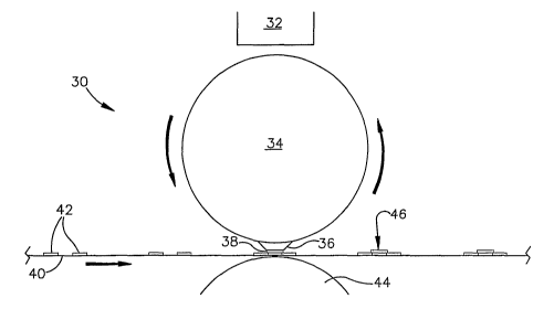
[0025] FIG. 2A is a side view of a single drum, one nozzle placement device
according to the present invention;
[0026] FIG. 2B is a side view of a single drum, one nozzle placement device
according to the present invention;
6
CA 02581425 2007-03-22
WO 2006/036666 PCT/US2005/033668
[0027] FIG. 3A is a graph illustrating a velocity profile of a transfer drum;
[0028] FIG. 3B is a graph illustrating a velocity profile of a transfer drum;
[0029] FIG. 4 is a side view of a single drum three nozzle placement device
according to the present invention;
[0030] FIG. 5 is a side view of a single drum three nozzle placement device
according to the present invention;
[0031]FIG. 6 is a flow chart showing a method of the present invention;
[0032] FIG. 7 is a side view of a two drum, three nozzle placement device
according
to the present invention;
[0033] FIG. 8 is an oblique view of a two drum, three nozzle placement device
according to the present invention;
[0034] FIG. 9 is a side view of a two drum, three nozzle placement device
showing
the primary drum and the secondary drum during transfer of a chip from the
primary
drum to the secondary drum;
[0035] FIG. 10 is a side view of a two drum, three nozzle placement device
showing
the secondary drum placing a chip onto an antenna structure on a web;
[0036] FIG. 11 is a side view of a two drum, three nozzle placement device
showing
the primary drum and the secondary drum during transfer of a chip from the
primary
drum to the secondary drum;
[0037] FIG. 12 is an exploded view of an embodiment of the invention; and
[0038] FIG. 13 is a schematic diagram of an embodiment of the invention.
DETAILED DESCRIPTION
[0039]A high-speed process includes removing RFID circuits from a carrier web
having a first pitch and transferring the RFID circuits to electrical
components, such
as RFID antenna structures, on a moving web having a second pitch. Typically,
the
second pitch is greater than the first pitch. According to one method, a
transfer
drum transfers RFID circuits to a moving web of electrical components, such as
antennas, by picking up a chip when the transfer drum is stationary, and
transferring
the chip to the moving web when the transfer drum is rotating such that a
tangential
velocity of the transfer drum is substantially equal to the linear velocity of
the moving
web. According to another method, a primary drum removes the RFID circuits
from
7
CA 02581425 2007-03-22
WO 2006/036666 PCT/US2005/033668
a carrier web having a first pitch, and transfers the RFID circuits to an
intermittently
or variably rotating secondary drum, which then places the RFID circuits onto
an
electrical component on a moving web having a second pitch.
[0040] In FIG. 1, a flow chart is shown depicting a method 5 of placing an
RFID
circuit onto an antenna on a moving web. The method 5 of FIG. 1 will be
described
in relation to a transfer drum having a single vacuum port or nozzle. However,
it will
be understood that the method 5 is equally applicable to any single nozzle of
a multi-
nozzle transfer drum. Further, while the method is described with reference to
nozzles or ports, the method does not require nozzles or ports.
[0041]The method 5 begins in process step 14 wherein a singulated chip is
picked
up by a nozzle on a transfer drum. In this embodiment, the transfer drum is
momentarily stationary when an RFID circuit is picked up by the nozzle in the
12
o'clock position on the transfer drum. In process step 16, the transfer drum
is
accelerated such that the tangential velocity of the nozzle is substantially
equal to
the linear velocity of a moving web of electronic components when the nozzle
reaches the 6 o'clock position. The RFID circuit is then transferred from the
nozzle
to the moving web of electronic components in process step 18. After the RFID
circuit is transferred to the moving web of electronic devices, the transfer
drum is
decelerated, in process step 20, such that the nozzle is returned to the 12
o'clock
position whereat the nozzle is in position to pick up another chip for
transfer to the
moving web of electrical components.
[0042] In one implementation of the nozzle of the transfer drum, the nozzle is
a
vacuum holder that engages and disengages RFID circuits using negative and
positive pressures. However, the invention also encompasses mechanical
securement of the RFID circuit to the transfer drum, and as used in this
patent
application the term "nozzle" encompasses not only vacuum securement but also
mechanical securement of RFID circuits.
[0043]Turning to FIGS. 2A and 2B, a high-speed placement device 30 is shown
including an RFID circuit supply device 32, such as a magazine, and a transfer
drum
34 having a single vacuum port or nozzle 36 for transferring RFID circuits 38
from
the supply device 32 to a web 40 of electronic components 42, and a base
roller 44.
As shown in FIG. 2A, the transfer drum 34 is positioned between the RFID
circuit
8
CA 02581425 2007-03-22
WO 2006/036666 PCT/US2005/033668
supply device 32 and a base roller 44 with the nozzle 36 at the 12 o'clock
position.
The base roller 44 typically rotates clockwise at a suitable speed thereby
advancing
the web 40 of electrical components 42 at a constant rate from left to right.
When
rotating, the transfer drum 34 rotates counterclockwise. In this embodiment,
the
nozzle 36, through selective application of negative pressure, picks an RFID
circuit
38 from the supply device 32 while the transfer drum 34 is momentarily
stationary
with the nozzle 36 at the 12 o'clock position. Once an RFID circuit 38 is
secured to
the nozzle 36, the transfer drum 34 rotates counter-clockwise accelerating to
a
placement velocity at which time the nozzle 36 and the RFID circuit 38 have a
tangential velocity substantially equal to the linear velocity of the moving
web 40. In
FIG. 2B, the nozzle 36 with RFID circuit 38 secured thereto is shown in the 6
o'clock
position with the transfer drum 34 rotating such that the tangential velocity
of the
nozzle 36 and/or RFID circuit 38 is substantially equal to the linear speed of
the
moving web 40. The RFID circuit 38 is then transferred to an electronic
component
42 on the web 40 by selective removal of the negative pressure and/or
application of
positive pressure. The RFID device 46 resulting from the combination of the
RFID
circuit 38 and the electronic component 42 continues moving on the web 40. The
transfer drum 34 may be situated such that the nozzle 36 forces the RFID
circuit 38
against the electrical component 42 on the web 40. After the RFID circuit 38
is
placed, the transfer drum 34 continues rotating counterclockwise thereby
returning
the nozzle 36 to the 12 o'clock position whereat the nozzle 36 is once again
stationary and in position to pick up another RFID circuit 38 from the supply
device
32.
[0044] In the present embodiment, the transfer drum accelerates from zero
revolutions per minute (RPM's) at the 12 o'clock position to the placing
velocity at
the 6 o'clock position and back to zero RPM's at the 12 o'clock position.
Thus, the
transfer drum 34 must accelerate from stationary to placing velocity within
180
degrees of rotation (i.e., between the 12 o'clock picking position and the 6
o'clock
placing position). It will be appreciated that the manner in which the placing
drum 34
is accelerated and decelerated during one revolution, also referred to herein
as the
velocity profile of the placing drum, may be any suitable manner depending on
a
variety of factors such as the total throughput rate of the placement device
30, the
9
CA 02581425 2007-03-22
WO 2006/036666 PCT/US2005/033668
rate at which RFID circuits 38 can be supplied to the transfer drum 34, the
minimum
time required for an RFID circuit 38 to be secured to a vacuum port or nozzle
36 of
the transfer drum 34, etc.
[0045] In an embodiment in which an RFID circuit is singulated and then
secured to
the transfer drum, the velocity profile of the transfer drum typically will
include a
dwell time, or time interval when the transfer drum is held stationary to
receive and
hold the singulated RFID circuit. FIGS. 3A and 3B show two exemplary velocity
profiles for the transfer drum. FIG. 3A shows a velocity profile with a
straight line
increase in velocity from stationary to full speed, while FIG. 3B shows an
example of
an arcuate velocity profile. Each of these transfer drum velocity profiles are
for
transfer drums with three nozzles, and the profiles include dwell regions at 0
,.120 ,
and 240 of the rotation cycle. Other transfer drum configurations may also
have
similar velocity profiles.
[0046]Turning now to FIGS. 4 and 5, a high-speed placement device 50 having a
three nozzle transfer drum 54 will be described. The nozzles 56a, 56b, 56c in
this
embodiment are arranged around the circumference of the transfer drum 54 at
120
degree intervals. Thus, nozzle 56a is positioned at 12 o'clock, nozzle 56b is
positioned at 8 o'clock, and nozzle 56c is positioned at 4 o'clock in FIG. 4.
An RFID
circuit supply device 52 is located above the 12 o'clock position of the
transfer drum
54. A web 60 of electrical components 62 moves from left to right below the
transfer
drum 54 via the base roller 64. In FIG. 4, the transfer drum 54 is momentarily
stationary allowing nozzle 56a to pick up an RFID circuit 58 from the supply
device
52.
[0047] Once the RFID circuit 58 is secured to nozzle 56a, the transfer drum 54
commences accelerating counter-clockwise rotation. In the three nozzle
configuration of the present embodiment, the transfer drum 54 must accelerate
from
stationary to placing velocity and then decelerate back to stationary through
an arc
of 120 degrees. Thus, as seen in FIG. 4, the transfer drum 54 must achieve
placing
velocity within the 60 degree arc A, thereby rotating nozzle 56b to the 6
o'clock
position for placing the RFID circuit 58 previously picked up from the RFID
circuit
supply device 52. The tangential velocity of the RFID circuit 52 secured to
nozzle
56b when it reaches the 6 o'clock position is substantially equal to the
linear velocity
CA 02581425 2007-03-22
WO 2006/036666 PCT/US2005/033668
of the moving web 60 of electronic components 62. An RFID device 66 is thus
formed on the web 60. After the RFID circuit 58 is placed, the transfer drum
54
decelerates to zero RPM's within the 60-degree arc B shown in FIG. 5, thereby
bringing nozzle 56c to the 12 o'clock position.
[0048] It will be appreciated that in the present embodiment, the transfer
drum 54
intermittently rotates in 120-degree intervals. During each 120 degree
rotation
interval, a first nozzle in the 12 o'clock position, which may be any one of
nozzles
56a, 56b,or 56c, picks up an RFID circuit 58 from the supply device 52 when
the
transfer drum 54 is stationary. The transfer drum 54 then accelerates through
an
arc of 60 degrees until a second nozzle 56a, 56b, or 56c as appropriate is
rotating
such that the tangential velocity of the nozzle is substantially equal to the
linear
velocity of the moving web 60, at which time an RFID circuit 58 is transferred
to an
electrical component 62 on the web 60. After the RFID circuit 58 is placed,
the
transfer drum 54 decelerates over a 60 degree arc until a third nozzle 56a,
56b, or
56c as appropriate is rotated into position to pick up an RFID circuit 58 from
the
supply device 52. It will be appreciated that other configurations of nozzles
and/or
multiple RFID circuit supply devices 52 are possible. Further, while the above
description begins with nozzle 56a in the 12 o'clock position, any one of the
nozzles
56a, 56b, or 56c could begin in the 12 o'clock position, with the remaining
two
nozzles assuming the remaining two relative positions as appropriate.
Therefore,
the above description describes but one of a many possible nozzle
configurations
that may be used in conjunction with the present invention.
[0049]As an alternative to the above described transfer drum configuration
including
three nozzles, other configurations and numbers of nozzles are possible.
Configurations with odd numbers of nozzles, evenly spaced around the transfer
drum, are compatible with the preferred type of velocity profile in which the
transfer
drum receives RFID devices at the 12 o'clock position while stationary,
accelerates
to the placing velocity at the 6 o'clock position and back to zero RPM's at
the 12
o'clock position (perhaps over a series of sub-cycles as in Figures 3A, 3B).
Configurations with even numbers of nozzle also are possible, however, such as
a
two nozzle configuration with dwell regions at nine o'clock (where RFID
circuits are
secured to the transfer drum) and at three o'clock. Increasing the number of
nozzles
11
CA 02581425 2007-03-22
WO 2006/036666 PCT/US2005/033668
beyond a few may be undesirable as it would reduce the angular interval over
which
transfer drum acceleration and deceleration would occur.
[0050] In FIG. 6, a flow chart is shown depicting a method 105 of placing an
RFID
circuit onto an antenna on a web at high speed using a two-drum piacement
device
according to the present invention. The method 105 begins in process step 114,
wherein an RFID circuit is picked by a primary drum. The primary drum may be
equipped with a vacuum source for providing suction for temporarily securing
the
RFID circuit to the primary drum. The RFID circuit is then transferred from
the
primary drum to the secondary drum in process step 116. The transfer of the
RFID
circuit from the primary drum to the secondary drum may occur while the
primary
drum and secondary drum are momentarily stationary, or while the primary drum
and secondary drum are rotating at substantially the same peripheral speed. In
process step 118, the secondary drum is accelerated or decelerated such that
the
peripheral speed of the secondary drum is substantially equal to the speed of
the
web of electronic components, such as antenna structures. The RFID circuit is
then
placed onto the antenna structure on the antenna web in process step 120. The
secondary drum is then accelerated or decelerated as appropriate, in process
step
122, such that the peripheral speed of the secondary drum is substantially
equal to
the peripheral speed of the primary drum thereby preparing for the transfer of
another RFID circuit from the primary drum to the secondary drum. After the
RFID
circuits are placed onto antenna structures, the RFID circuits subsequently
may be
coupled with the antenna structure in any suitable manner. The method 105 will
further be described below with reference to FIGS. 7-13.
[0051] In FIGS. 7 and 8, a high speed placement device 200 is shown. A web 220
of
antenna structures 222 advances from left to right below the device 200 in
both
figures. A web 250 carrying RFID circuits 252 enters the high-speed placement
device 200 through slot 260. An RFID circuit 252 is removed from the web 250
at
peel tip 262, and the web 250 exits the device 200 at slot 264. As an RFID
circuit
252 is separated from the web 250 at peel tip 262, it is picked up by the
primary
drum 270. The primary drum 270 may hold the RFID circuit 252 with a vacuum
applied through a plurality of primary nozzles 273 in the primary drum surface
272.
A plurality of recesses 274 and/or ridges 275 are also shown on the primary
drum
12
CA 02581425 2007-03-22
WO 2006/036666 PCT/US2005/033668
surface 272 for receiving the RFID circuits 252.
[0052] In the embodiment shown in FIGS. 7 and 8, the primary drum 270 rotates
in a
clockwise manner while the secondary drum 280 rotates counterclockwise. As the
primary drum 270 rotates, an RFID circuit 252 picked by the primary drum 270
approaches the transfer position 276. The transfer position 276 in the
illustrated
embodiment corresponds to the six o'clock position of the primary drum 270 and
the
twelve o'clock position of the secondary drum 280. Other transfer positions
are
possible, such as a transfer position corresponding to the four o'clock
position of the
primary drum 270 and the 10 o'clock position of the secondary drum 280.
Similarly,
more than one primary drum may be positioned around the periphery of the
secondary drum thereby enabling transfer of RFID circuits 252 to the secondary
drum 280 at more than one location. For example, a secondary drum 280 may have
two primary drums positioned at the two o'clock and ten o'clock positions of
the
secondary drum 280, respectively.
[0053]At the transfer position 276, an RFID circuit 252 is transferred from
the
primary drum 270 to the secondary drum 280. Prior to the transfer of the RFID
circuit 252 from the primary drum 270 to the secondary drum 280, the secondary
drum 280 is accelerated or decelerated such that, at the time of the transfer,
the
peripheral speed of the secondary drum's surface 282 is substantially equal to
the
peripheral speed of the surface 272 of the primary drum 270.
[0054]To facilitate the transfer of the RFID circuit 252 from the primary drum
270 to
the secondary drum 280, the vacuum source in the primary drum 270 is released
thereby removing the holding force on the RFID circuit 252 at surface 272. In
addition, a vacuum source in drum 280 is activated to secure the RFID circuit
252 to
its surface 282. To assist the release of the RFID circuit 252 from the
primary drum
270, a positive pressure may be applied by the primary drum 270 thereby
providing
a separating force to the RFID circuit 252 at surface 272. The primary drum
270
and secondary drum 280 may be stationary during the transfer process of the
RFID
circuit 252 from surface 272 to surface 282, or alternatively the primary drum
270
and secondary drum 280 may rotate during the transfer of the RFID circuit 252.
[0055]As the web 220 of antenna structures 222 advances'from left to right, an
antenna structure 222 moves into the placing position 290 for accepting an
RFID
13
CA 02581425 2007-03-22
WO 2006/036666 PCT/US2005/033668
circuit 252. As the antenna structure 222 enters the placing position 290, the
secondary drum 280 accelerates or decelerates as appropriate such that the
peripheral speed of the surface 282 of the secondary drum 280 is substantially
equal
to the speed of the web 220. The rotation and speed of drum 280 is timed such
that
the RFID circuit 252 held to surface 282 contacts the antenna structure 222 on
the
web 220 at the placement position 290. At this time the vacuum source in the
secondary drum 280 is removed and the RFID circuit 252 is placed onto the
antenna
structure 222 on the moving web 220. A positive pressure may be applied by the
secondary drum 280 thereby providing a separating force to the RFID circuit
252 at
surface 272.
[0056]The web 220 may include an adhesive or other means for securing the RFID
circuit 252 to the antenna structure 222, thereby facilitating the transfer of
the RFID
circuit 252 from the secondary drum surface 282 to the antenna structure 222
on the
web 220. For example, an adhesive may be applied to the web 220, the antenna
structure 222, or both prior to the antenna structure 222 reaching the
placement
position 290. Typically, the secondary drum 280 need not make contact with the
web 220 or the antenna structure 222 during the placement of the RFID circuit
252
to the antenna structure 222. However, in some instances, such as when a
pressure sensitive adhesive is to be used to couple the RFID circuit 252 to
the
antenna structure 222, the secondary drum 280 may make contact with the web
220
and/or antenna structure 222 thereby providing pressure to activate the
pressure
sensitive adhesive. For this purpose, a backing roller or other member, such
as
shown at 44 in FIGS. 2A, 2B, 64 in FIGS. 4, and 5, and at 295 in FIGS. 7-10
may
form a pressure nip to facilitate transfer of the RFID circuit to the web.
[0057]Turning now to FIGS. 9-11, the operation of the placing device 200, in
particular the primary and secondary drums 270 and 280, will be described in
detail.
In FIG. 9, the primary drum 270 and secondary drum 280 are shown. The primary
drum 270 includes a plurality of primary nozzles 273, recesses 274, and/or
ridges
275 for receiving an RFID circuit 252. The primary drum 270 further includes a
vacuum source for directing suction to the primary drum surface 272 for
temporarily
securing RFID circuits 252 thereto. The primary drum 270 in this embodiment
rotates clockwise. RFID circuits 252 are shown secured to the primary drum 270
via
14
CA 02581425 2007-03-22
WO 2006/036666 PCT/US2005/033668
the suction provided by the vacuum source. As the primary drum 270 rotates
clockwise, the RFID circuits 252 secured to the primary drum surface 272
rotate into
the transfer position 276 where they are transferred to the secondary drum
280.
The primary drum 270 may rotate continuously, intermittently, or variably
depending
on the particular application.
[0058] In the illustrated embodiment, the secondary drum 280 includes three
secondary nozzles 284a, 284b, 284c disposed at 120 degree intervals around the
surface 282 of the secondary drum 280. It will be appreciated that in practice
any
suitable number of secondary nozzles may be used; however, for simplicity of
explanation three secondary nozzles are shown. The secondary drum 280 also
includes a vacuum source for directing suction to the secondary nozzles for
temporarily securing RFID circuits 252 to the secondary nozzles.
[0059] In FIG. 9, a primary nozzle 273 and secondary nozzle 284a are in the
transfer
position 276. In the transfer position 276, the axes of a primary nozzle 273
and
secondary nozzle 284a are aligned. Secondary nozzle 284b is shown with a chip
252 secured to it. Secondary nozzle 284c does not have a chip secured to it.
The
web 220 of antenna structures 222 is shown below the secondary drum 280 and
advances from left to right in FIGS. 9 and 10.
[0060] In FIG. 10, the secondary drum 280 has been rotated approximately 60
counterclockwise from the position shown in FIG. 9. Secondary nozzle 284a is
now
shown with an RFID circuit 252 secured to it, the RFID circuit 252 having been
transferred from the primary drum 270 as shown in FIG. 9. Secondary nozzle
284b
is now in the placing position 290. Secondary nozzle 284c, having just placed
an
RFID circuit 252 onto an antenna structure 222 as shown in FIG. 9, is
approaching
the transfer position 276 where another RFID circuit 252 will be transferred
thereto.
In FIG. 10, the web 220 has advanced from left to right such that an antenna
structure 222 is in the placing position 290. At this moment, the peripheral
speed of
the secondary drum 280 and/or secondary nozzle 284b is substantially equal to
the
speed of the web 220, the secondary drum having been accelerated or
decelerated
such that the peripheral speed of secondary nozzle 284b is substantially equal
to the
speed of the web 220. Thus, while the web 220 may be advancing at high speed,
there is essentially no relative motion between secondary nozzle 284b and the
web
CA 02581425 2007-03-22
WO 2006/036666 PCT/US2005/033668
220. When secondary nozzle 284b is in the placing position 290, the vacuum
source supplying suction to secondary nozzle 284b is removed, thereby
eliminating
the force securing the RFID circuit 252 to secondary nozzle 284b, and the RFID
circuit 252 is placed onto the antenna structure 222. -
[0061]After placing the RFID circuit 252 onto the antenna structure 222, the
secondary drum 280 continues rotating counterclockwise such that secondary
nozzle 284c advances into the transfer position 276, as shown in FIG. 11. As
secondary nozzle 284c approaches the transfer position 276, the secondary drum
280 is accelerated or decelerated such that the peripheral speed of secondary
nozzle 284c of the secondary drum 280 is substantially equal to the peripheral
speed of the surface 272 and/or primary nozzle 273 of the primary drum 270 at
the
transfer position 276. As previously mentioned, the primary drum 270 and
secondary drum 280 may be momentarily stationary during the transfer step.
[0062] It will be appreciated that the indexing of an RFID circuit 252 to an
antenna
structure 222 is achieved by the variable rotation, or acceleration and/or
deceleration, of the primary drum 270 and/or secondary drum 252. Thus, the two-
drum placing device of the present embodiment may allow indexing of RFID
circuits
to electrical components having a greater pitch than a single drum placing
device
because both the primary and secondary drum can perform a portion of the
indexing
function. The primary drum may rotate intermittently to perform an indexing
function
in the same manner in which the secondary drum rotates intermittently to index
the
RFID circuit to the web of electrical components.
[0063]Turning to FIG. 12, an exploded view is shown of a high speed placement
device 300 according to another embodiment of the invention. The device 300
includes a peel point 362, two primary drums 370, and a secondary drum 380. In
this embodiment, the two primary drums 370 transfer RFID circuits to the
secondary
nozzles 384a, 384b, and 384c (384c not shown in FIG. 12) of the secondary drum
380. In this configuration, the secondary drum 380 may place RFID circuits to
a web
having more than one lane of antenna structures. The device 300 further
includes
end plates 390 on each side of the primary drums 370. Bearings 402 support the
secondary drum 380, and the upper and lower housing 412 and 414 enclose the
device.
16
CA 02581425 2007-03-22
WO 2006/036666 PCT/US2005/033668
[0064] In FIG. 13, a schematic diagram illustrates a speed placement device
400
including a primary drum 470, a motor 478 coupled to the primary drum 470, and
a
vacuum source 479 coupled to the primary drum 470. The secondary drum 480
includes a motor 488 and a vacuum source 489 coupled thereto. It will also be
appreciated that a singie motor and a single vacuum source may be coupied to
both
the primary drum 470 and the secondary drum 480. Any suitable motor may be
used to provide rotational force to the drums. For example, electric or
hydraulic
motors may be coupled to the drums to provide rotational force. In addition,
suitable
gearing and transmission assemblies may be used to couple a motor or other
drive
means to the drums.
[0065] It will be appreciated that any suitable number of primary drums may be
used
to transfer chips or straps to one or more secondary drums. The primary drums
may
be arranged along a common axis to transfer RFID circuits to one or more
secondary drums as shown in FIG. 12, thereby allowing the simultaneously
placement of more than one RFID circuit to a plurality of antenna structures
in more
than one lane on one or more webs. It will further be appreciated that more
than
one primary drum may transfer RFID circuits to a secondary drum, wherein the
primary drums are arranged at different peripheral locations around the
circumference of the secondary drum.
[0066] It will also be appreciated that the relative speeds of the primary
drum(s) and
secondary drum(s) in any of the above embodiments may be controlled by
suitable
gears and/or electric motors. For example, stepper motor drives may be used to
control the relative speeds of the drums. The use of stepper motor drives with
computer or other digital controls may be advantageous by allowing for the
simple
adjustment of the high-speed placement device to accommodate RFID circuit webs
and antenna webs having a wide variety of component pitches.
[0067] In a typical application of RFID circuits to antenna structures, the
secondary
drum will be accelerated when a secondary nozzle is rotated between the
transfer
position and the placement position such that the peripheral speed of a
particular
secondary nozzle is greater at the placement position than at the picking
position.
Because the peripheral speed of the secondary nozzles at the placement
position
may be adjusted, and the rate of advancement of the web of antenna structures
may
17
CA 02581425 2007-03-22
WO 2006/036666 PCT/US2005/033668
be adjusted, the present invention allows the placement of RFID circuits to
antenna
structures on webs having a wide variety of pitches.
[0068] It will further be appreciated that, to aid in placement of the RFID
circuits onto
the antenna structures, vision systems may be employed to read fiducial marks
and/or antenna positions and provide feedback to the control systems
controlling the
primary and secondary drums, the RFID circuit carrier web, and/or the web of
antenna structures. Further, methods other than a peel tip may be used to
singulate
the RFID circuits from the carrier web. For example, the carrier web may be
die cut
thereby singulating the RFID circuits prior to picking by a primary drum.
Alternatively, the carrier web may pass between a cutter member and a primary
drum, wherein the cutter member singulates the RFID circuits by cutting the
web
using the primary drum as an anvil.
[0069]The placing device described above allows RFID circuits of a first pitch
(typically, relatively small) on a first carrier web to be transferred to
antennas or other
electrical components on second web having a second pitch (typically,
relatively
large), with no change in speed of the second web. The RFID circuit carrier
web
may have constant, intermittent or variable speed as required to provide a
suitable
number of RFID circuits to the primary drum. Similarly, the primary drum may
have
constant, intermittent, or variable rotational speed as required to receive
adequate
RFID circuits from the carrier web and supply adequate RFID circuits to the
secondary drum.
[0070] It will be appreciated that in any one of the above embodiments, the
tangential or peripheral velocity of an RFID circuit secured to a drum may be
substantially equal to the linear velocity of a moving web during placement.
Throughout the foregoing description, reference has been made to a tangential
or
peripheral velocity of a drum's surface being substantially equal to the a
linear
velocity of a web when an RFID circuit is placed onto an electrical component
on the
web. However, in some configurations, particularly in a configuration
employing
nozzles that extend outward from the peripheral surface of a drum, it will be
appreciated that it is the tangential velocity of the nozzles and/or RFID
circuits
secured thereto that is substantially equal to the linear velocity of the
moving web of
electrical components. Therefore, it will be understood that a drum's surface
is
18
CA 02581425 2007-03-22
WO 2006/036666 PCT/US2005/033668
intended to be the surface to which an RFID circuit is secured.
[0071]Certain modifications and improvements wili occur to those skilled in
the art
upon a reading of the foregoing description. It should be understood that the
present invention is not limited to any particular type of wireless
communication
device, or interposers. The term "electronic component" may corriprise an
electrical
circuits or electrical device, and in the preferred embodiment comprises an
antenna.
The antenna may include a single antenna portion, or a plurality of separate
antenna
portions. Further, a wide variety of antenna designs may be used with the
present
invention such as loop, slot, or patch antennas. For the purposes of this
application,
couple, coupled, or coupling may encompass both mechanical coupling and
electrical coupling. Mechanical coupling includes physically securing the
interposer
to an electronic component. Electrical coupling includes forming an electrical
connection between the interposer and electronic component. An electrical
connection includes directly connecting or reactively coupling an interposer
to an
electronic component. Reactive coupling is defined as either capacitive or
inductive
coupling, or a combination of both. Capacitive coupling may involve putting
the
interposer into close proximity with an electronic component, with dielectric
pads
therebetween, to allow capacitive coupling between the interposer and the
electronic
component. The dielectric pads may include a non-conductive adhesive, such as
a
pressure-sensitive adhesive, for example Fasson adhesives S4800 and S333
available from Avery Dennison Corporation, and a high dielectric constant
material,
such as a titanium compound, for example titanium dioxide or barium titanate.
The
dielectric pads have an effective dielectric constant that is a non-constant
function of
thickness of the dielectric pads. For example, the dielectric pads may include
conductive particles, such as aluminum and/or nickel particles, to minimize
the effect
of changes in thickness on the capacitive coupling. The dielectric pads may
have a
thickness of about 0.025 mm (0.001 inches) or less.
[0072]The methods of the invention, though described in relation to RFID
chips,
strap, interposers and antenna structures, may be advantageous for placing
chips
directly to antennas or placing chips onto interposer leads. For example, in
any of
the above embodiments, interposer leads may be substituted for an antenna
structure and a chip may be placed onto the interposer leads instead of an
antenna
19
CA 02581425 2007-03-22
WO 2006/036666 PCT/US2005/033668
structure.
[0073] One of ordinary skill in the art will recognize that there are
different manners
in which these elements can accomplish the present invention. The present
invention is intended to cover what is ciaimed and any equivalents. The
specific
embodiments used herein are to aid in the understanding of the present
invention,
and should not be used to limit the scope of the invention in a manner
narrower than
the claims and their equivalents.
[0074]Aithough the invention has been shown and described with respect to a
certain embodiment or embodiments, it is obvious that equivalent alterations
and
modifications will occur to others skilled in the art upon the reading and
understanding of this specification and the annexed drawings. In particular
regard to
the various functions performed by the above described elements (components,
assemblies, devices, compositions, etc.), the terms (including a reference to
a
"means") used to describe such elements are intended to correspond, unless
otherwise indicated, to any element which performs the specified function of
the
described element (i.e., that is functionally equivalent), even though not
structurally
equivalent to the disclosed structure which performs the function in the
herein
illustrated exemplary embodiment or embodiments of the invention. In addition,
while a particular feature of the invention may have been described above with
respect to only one or more of several illustrated embodiments, such feature
may be
combined with one or more other features of the other embodiments, as may be
desired and advantageous for any given or particular application.