Note: Descriptions are shown in the official language in which they were submitted.
CA 02581524 2007-03-06
DATA PROCESSING APPARATUS
BACKGROUND OF THE INVENTION
1. Field of the Invention
The present invention relates to a data processing
apparatus including a plurality of CPU (Central Processing Unit)
modules which are operated synchronously with each other.
2. Description of the Related Art
A data processing apparatus including a plurality of CPU
modules which are operated synchronously with each other is known.
The synchronization between the CPU modules is conventionally
performed by inputting a clock from a clock source that is common
to all of the CPU modules. However, such a data processing
apparatus has a problem in that the operations of all the CPU
modules are stopped when a fault occurs in the common clock source.
To cope with the problem, for example, in the data
processing apparatus as disclosed in JP 07-73059 A, each of the
CPU modules recognizes the values of the mutual clock counters,
and the CPU modules which are respectively operated based on
the clocksfrom the individual clock sources are made synchronous
with each other.
In this case, each CPU module transmits and receives the
value of the mutual clock counter as a packet to and from the
other CPU modules. In that case, each CPU module cannot execute
the exact synchronizing process, unless the arrival time of its
counter packet is constant. When the counter packet is
transmitted and received through a general signal line, the
counter packet receives the influence of a general packet, and
CA 02581524 2007-03-06
2
an arrival time thereof is not constant. Thus, when the counter
packet is transmitted and received through the general signal
line, the data processing apparatus must include a dedicated
configuration, for example, a configuration in which the counter
packet is preferentially processed without any influence of the
general packet. Alternatively, the data processing apparatus
must include the signal line dedicated to the clock counter
information, which is different from the general signal line,
to transmit and receive the general packet and the like. In
any case, the configuration of the data processing apparatus
becomes large in scale and complex.
SUMMARY OF THE INVENTION
The present invention has been made to solve the
above-mentioned problems. An exemplary feature of the present
invention is to provide a data processing apparatus capable of
synchronizing a plurality of CPU modules each being operated
at an independent clock, with a simple configuration.
In an aspect of the present invention, a data processing
apparatus includes a plurality of CPU modules each including
a CPU. The plurality of CPU modules are connected to each other
through a cross link. Each of the plurality of CPU module
includes a clock source which supplies a clock to the CPU of
its own, a clock counter which counts the clocks from the clock
source, an I/0 module which transmits and receives a
predetermined packet to and from the CPU, a first data adder
which, when a packet designated to the CPU is received from the
I/0 module, reads a value of the clock counter, adds a
CA 02581524 2007-03-06
3
predetermined offset value to the read value to generate a timing
value, and adds the generated timing value to the packet
designated to the CPU, and a timing adjuster which adjusts timing
of transmitting the packet to the CPU, based on the timing value
of the packet received from the first data adder and the value
of the clock counter.
The CPU module constituting the data processing apparatus
of the present invention adds the timing value for defining its
processing timing of to the packet to be transmitted to the CPU
from the I/0 module, and processes the packet based on the value
of the clock counter of its own and the timing value. Thus,
the data processing apparatus makes it possible to synchronize
the plurality of CPU modules each being operated at the
independent clock.
Further, the data processing apparatus of the present
invention is operated based on the timing value added to the
packet and the value of the clock counter of each CPU module.
Thus, the counter value of the synchronous partner is not required
to be known. Consequently, according to the data processing
apparatus of the present invention, there is no need for the
general signal line to be provided with the special configuration
to prevent a counter packet from receiving the influence of the
general packet. Also, there is no need for the data processing
apparatus to be provided with the signal line dedicated to the
counter packet between the CPU modules.
BRIEF DESCRIPTION OF THE DRAWINGS
The above and other objects, features and advantages of
CA 02581524 2007-03-06
4
the present invention will become more apparent from the
following detailed description when taken in conjunction with
the accompanying drawings wherein:
FIG. 1 shows an example of a control block diagram of a
data processing apparatus according to a first embodiment of
the present invention;
FIG. 2 shows an example of a sequence diagram for
illustrating an operation of resetting a CPU and a clock counter
of each CPU module in the data processing apparatus shown in
FIG. 1;
FIG. 3 shows an example of a sequence diagram for
illustrating an operation performed in the data processing
apparatus shown in FIG. 1, in which the CPU transmits a request
packet to an I/O module and receives a response packet for the
request packet from the I/0 module;
FIG. 4 shows an example of a sequence diagram illustrating
an operation performed in the data processing apparatus shown
in FIG. 1, in which the I/0 module transmits a request packet
to the CPU and receives a response packet for the request packet
from the CPU;
FIG. 5 shows an example of a sequence diagram illustrating
an operation performed in the data processing apparatus shown
in FIG. 1, the CPU receives an interruption packet periodically
transmitted from the I/0 module and resets the clock counter
in response to the interruption packet;
FIG. 6 is a graph explicitly showing a fact that a clock
counter deviation amount between the CPU modules fall in a certain
range by the periodical resetting process explained with
CA 02581524 2007-03-06
reference to FIG. 5; and
FIG. 7 shows an example of a control block diagram of a
data processing apparatus according to a second embodiment of
the present invention.
5
DETAILED DESCRIPTION OF THE EXEMPLARY EMBODIMENTS
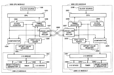
FIG. 1 shows an example of a control block diagram of a
data processing apparatus according to a first embodiment of
the present invention. The data processing apparatus includes
a CPU module 1000 and a CPU module 2000. The CPU module 1000
and the CPU module 2000 are connected through a cross link 3000.
The CPU module 1000 includes a clock source 1100, a CPU
1201, a clock counter 1202, an offset value register 1203, a
comparator 1204, a first data adder 1205, a timing adjuster 1206,
a cross link controller 1207 and an I/0 module 1300.
The CPU 1201 executes a series of command rows, and is
composed of, for example, CPU (central processing unit) and its
peripheral circuit.
The clock counter 1202 counts the clocks from the clock
source 1100. The clock counter 1202 resets the counter value
when receiving a reset instruction of a counter value from the
timing adjuster 1206. Usually, the clock counter 1202 and a
clock counter 2202 in the CPU module 2000 are reset when the
CPU 1201 and a CPU 2201 in the CPU module 2000 start a synchronizing
operation.
The offset value register 1203 stores a preset offset value.
The offset value is a value equal to or greater than the necessary
minimum number of the clocks, for example, until the packet
CA 02581524 2007-03-06
6
transmitted from the first data adder 1205 in the CPU module
1000 is received by a timing adjuster 2206 in the CPU module
2000 through the cross link 3000.
The comparator 1204 checks whether or not the packet
received from the CPU 1201 and the packet received from the CPU
2201 in the CPU module 2000 through the cross link 300 are
coincident. If the packets are coincident with each other, the
comparator 1204 chooses one of the packets and transmits it to
the I/0 module 1300. In this case, the comparator 1204 can also
buffer the packet transmitted from the CPU 1201 and the packet
transmitted from the CPU 2201.
The first data adder 1205 reads the value of the clock
counter 1202 when receiving the packet designated to the CPU
from the I/0 module 1300, adds the value of the offset value
register 1203 to that value to generate a timing value, and then
adds the generated timing value to the packet. The first data
adder 1205 transmits the packet with the timing value to the
timing adjuster 1206 and the cross link controller 1207.
The timing adjuster 1206 receives the packet added with
the timing value from the first data adder 1205 in the CPU module
1000 or a first data adder 2205 in the CPU module 2000. Then,
the timing adj uster 1206 waits until the value of the clock counter
1202 becomes coincident with the timing value added to the
received packet, and transmits the packet to the CPU 1201 when
they are coincident with each other. It should be noted that
the timing adjuster 1206 executes a control so that the processing
order of the packets is not different between the CPU modules
1000 and 2000 when the timing values of the packet received from
CA 02581524 2007-03-06
7
the first data adder 1205 in the CPU module 1000 and the packet
received from the first data adder 2205 in the CPU module 2000
are coincident with each other. For example, the timing adjuster
1206 can buffer the packet received from the first data adder
1205 and the packet received from the first data adder 2205.
The cross link controller 1207 transmits the packet
transmitted from the CPU 1201 to a comparator 2204 in the CPU
module 2000 through the cross link 3000 and a cross link controller
2207 in the CPU module 2000. Also, the cross link controller
1207 transmits the packet transmitted from the first data adder
1205 to the timing adjuster 2206 through the cross link 3000
and the cross link controller 2207. Moreover, the cross link
controller 1207 receives the packet transmitted from the CPU
2201 in the CPU module 2000 through the cross link controller
2207 and the cross link 3000, and transmits to the comparator
1204. Further, the cross link controller 1207 receives the
packet transmitted from the first data adder 2205 in the CPU
module 2000 through the cross link controller 2207 and the cross
link 3000, and transmits to the timing adjuster 1206.
The I/0 module 1300 includes an I/0 bridge 1301, a reset
packet generator 1302, a timer 1303 and an I/0 device 1304. The
I/0 bridge 1301 receives the packet from the comparator 1204
and transmits the packet to at least one of the reset packet
generator 1302, the timer 1303 and the I/0 device 1304. Further,
the I/0 bridge 1301 receives the packets transmitted from the
reset packet generator 1302, the timer 1303 and the I/0 device
1304, and transmits the packet to the first data adder 1205.
The reset packet generator 1302 generates the reset packet when
CA 02581524 2007-03-06
8
the generation of a reset packet is required by the CPUs 1201
and 2201, and transmits the packet to the first data adder 1205
through the I/0 bridge 1301. The timer 1303 generates a timer
interruption packet for each elapse of a predetermined time,
and transmits the packet to the first data adder 1205 through
the I/0 bridge 1301. The I/0 device 1304 is composed of an SCSI
controller, a LAN adapter and the like.
The CPU module 2000 includes a clock source 2100, the CPU
2201, the clock counter 2202, an offset value register 2203,
the comparator 2204, the first data adder 2205, the timing
adjuster 2206, the cross link controller 2207, and an I/O module
2300. Since those members are equal to those of the CPU module
1000, the explanations thereof are omitted.
It should be noted that the respective CPUs 1201, 2201
can discriminate the I/0 modules 1300, 2300, respectively.
However, since the CPU 1201 and the CPU 2201 are synchronously
operated, they are recognized as one CPU from the respective
I/0 modules 1300 and 2300, and both of them cannot be
discriminated.
The cross link 3000 establishes the connection between
the CPU module 1000 and the CPU module 2000. The cross link
3000 is composed of a parallel interface such as a PCI bus, and
a serial interface such as PCI-Express, and the like. The cross
link 3000 is essential for the data processing apparatus having
the plurality of CPU modules, and is not a special signal line.
FIG. 2 shows an example of a sequence diagram illustrating
the operation of resetting the CPU 1201 and clock counter 1202
in the CPU module 1000, and the CPU 2201 and clock counter 2202
CA 02581524 2007-03-06
9
in the CPU module 2000 in the data processing apparatus of the
first embodiment of the present invention.
The resets of the clock counter 1202 and CPU 1201 in the
CPU module 1000 and the clock counter 2202 and CPU 2201 in the
CPU module 2000 are executed based on the reset packet transmitted
from the reset packet generator 1302 in the CPU module 1000 or
a reset packet generator 2302 in the CPU module 2000.
The reset packet generator 1302 or the reset packet
generator 2302 generates the reset packet when receiving a reset
request packet from the CPU 1201 or the CPU 2201. There are
no restrictions on whether the data processing apparatus carries
out the reset using the reset packet generator 1302 or the reset
packet generator 2302. Hereinafter, there is exemplified as
a case where the reset packet generator 1302 in the CPU module
1000 is used to reset the clock counter 1202 and CPU 1201 in
the CPU module 1000 and the clock counter 2202 and CPU 2201 in
the CPU module 2000.
First, the CPU 1201 transmits the reset request packet
to the comparator 1204 (Step S201) . At this time, the CPU 1201
and the CPU 2201 are not synchronous with each other. Accordingly,
the comparator 1204 transmits the reset request packet to the
reset packet generator 1302 in the I/0module 1300 without waiting
for the transmission of the same packet from the CPU 2201 (Step
S202).
The reset packet generator 1302 generates the reset packet
when receiving the reset request packet, and transmits the reset
packet to the first data adder 1205 (Step S203) . The first data
adder 1205 transmits the reset request packet to the timing
CA 02581524 2007-03-06
adjuster 1206 and the cross link controller 1207 when receiving
the reset packet from the reset packet generator 1302 (Step S204 ).
The timing adjuster 1206 refers to a transmission source
of the received reset packet, and judges whether or not the reset
5 packet is passed through the cross link 3000. In this case,
the transmission source of the reset packet is the reset packet
generator 1302, and the reset packet is not passed through the
cross link 3000. Accordingly, the timing adjuster 1206, after
waiting for the elapse of a preset clock cycle (Step S205) , resets
10 the clock counter 1202 (Step S206). After that, the timing
adjuster 1206 resets the CPU 1201 (Step S207).
On the other hand, the cross link controller 1207 transmits
the reset packet received from the first data adder 1205 to the
cross link controller 2207 through the cross link 3000 (Step
S208) The cross link controller 2207 transmits the received
reset packet to the timing adjuster 2206 (Step S209).
The timing adjuster 2206 refers to a transmission source
ID of the received reset packet, and judges whether or not the
reset packet is passed through the cross link 3000. In this
case, the transmission source is the reset packet generator 1302
in the CPU module 1000, and the reset packet is passed through
the cross link 3000. For this reason, the timing adjuster 2206
does not enter into a waiting state and immediately resets the
clock counter 2202 (StepS210) . Moreover, afterthat, thetiming
adjuster 2206 resets the CPU 2201 (Step S211).
By the above-mentioned operations, the clock deviation
between the clock counter 1202 and the clock counter 2202 is
removed. After that, the synchronous operation between the CPUs
CA 02581524 2007-03-06
11
1201 and 2201 is started.
FIG. 3 shows an example of a sequence diagram illustrating
the operation in which the CPU 1201 and the CPU 2201 transmit
a request packet to the I/0 module 1300 and receive a response
packet for the request from the I/0 module 1300.
First, the CPU 1201 transmits the request packet designated
to the I/0 module 1300 to the comparator 1204 (Step S301) . It
should be noted that the value of the clock counter 1202 in this
case is, for example, 10. It should be noted that the CPU 1201
and the CPU 2201 synchronously execute the same command row.
Thus, the CPU 2201 also transmits the request packet designated
to the I/O module 1300 to the cross link controller 2207 when
the value of the clock counter 2202 becomes 10 (Step S302) . The
cross link controller 2207 transmits the received request packet
to the cross link controller 1207 through the cross link 3000
(Step S303). The cross link controller 1207 transmits the
received request packet to the comparator 1204 (Step S304).
The comparator 1204 compares the response packet received
from the CPU 1201 and the response packet received from the CPU
2201 (Step S305). When a fault is not generated in the data
processing apparatus, these two request packets are coincident.
The comparator 1204 chooses one of the request packets and
transmits the request packet to the I/0 module 1300 (Step S306) .
The I/0 module 1300 judges whether or not the received
packet is the packet requiring a response. In this case, the
received packet is the request packet. Thus, the I/0 module
1300 generates a response packet and transmits the generated
packet to the first data adder 1205 (Step S307).
CA 02581524 2007-03-06
12
The first data adder 1205 refers to the clock counter 1202
(Step S308) when receiving the respons~- packet. It should be
noted that the value of the clock counter 1202 at this time is,
for example, 30. Besides, the value of the offset value register
1203 is, for example, 20. The first data adder 1205 adds the
value (=20) of the offset value register 1203 to the value (=30)
of the clock counter 1202 and adds its value as a timing value
TV (=50) to the response packet. The first data adder 1205
transmits the response packet, added with the timing value TV
to the timing adjuster 1206 and the cross link controller 1207
(Step S309).
The timing adjuster 1206 refers to the timing value TV
added to the response packet when receiving the response packet,
and executes the waiting until the value of the clock counter
1202 becomes equal to the timing value TV (Step S310 ). The timing
adjuster 1206 transmits the response packet to the CPU 1201 when
the value of the clock counter 1202 becomes equal to the timing
value TV (Step S311).
On the other hand, the cross link controller 1207 transmits
the response packet received from the first data adder 1205,
through the cross link 3000 to the cross link controller 2207
(Step S312). The cross link controller 2207 transmits the
received response packet to the timing adjuster 2206(Step S313).
The timing adjuster 2206 refers to the timing value TV
added to the response packet when receiving the response packet,
and executes the waiting until the value of the clock counter
2202 becomes equal to the timing value TV (Step S314 ). The timing
adjuster 2206 transmits the response packet to the CPU 2201 when
CA 02581524 2007-03-06
13
the value of the clock counter 2202 becomes equal to the timing
value TV (Step S315).
As described above, both of the CPU 1201 and the CPU 2201
transmit the request packet when the values of the clock counter
1202 and the clock counter 2202 are 10, and receive the response
packet when the values of the clock counter 1202 and the clock
counter 2202 are 50.
FIG. 4 shows an example of a sequence diagram illustrating
the operation in which the I/0 module 1300 transmits the request
packet to the CPU 1201 and the CPU 2201 and receives the response
packet for the request packet from the CPU 1201 and the CPU 2201.
The I/0 module 1300 transmits the request packets
designated to the CPU 1201 and the CPU 2201, to the first data
adder 1205 (Step S401). The first data adder 1205 refers to
the clock counter 1202 when receiving the request packet from
the I/0 module 1300 (Step S402) It should be noted that the
value of the clock counter 1202 in this case is, for example,
30. Besides, the value of the offset value register 1203 is,
for example, 20. The first data adder 1205 adds the value (=20)
of the offset value register 1203 to the value (=30) of the clock
counter 1202 and adds the value as the timing value TV (=50)
to the request packet. The first data adder 1205 transmits the
request packet added with the timing value TV to the timing
adjuster 1206 and the cross link controller 1207 (Step S403) .
The timing adjuster 1206 refers to the timing value TV
added to the request packet when receiving the request packet,
and executes the waiting until the value of the clock counter
1202 becomes equal to the timing value TV (= 50 )(Step S404)
CA 02581524 2007-03-06
14
The timing adjuster 1206 transmits the request packet to the
CPU 1201 when the value of the clock counter 1202 becomes equal
to the timing value TV (Step S405).
On the other hand, the cross link controller 1207 transmits
the request packet received fromthe first data adder 1205 through
the cross link 3000 to the cross link controller 2207 (Step S406) .
The cross link controller 2207 transmits the received request
packet to the timing adjuster 2206 (Step S407).
The timing adjuster 2206 refers to the timing value TV
added to the request packet when receiving the request packet,
and executes the waiting until the value of the clock counter
2202 becomes equal to the timing value TV (Step S408 ). The timing
adjuster 2206 transmits the response packet to the CPU 2201 when
the value of the clock counter 2202 becomes equal to the timing
value TV (Step S409).
The CPU 1201 judges whether or not the received request
packet is the packet requiring the response, and transmits the
response packet to the comparator 1204 when the response is
required (Step S410).
On the other hand, the CPU 2201 judges whether or not the
received request packet is the packet requiring the response,
and if the response is required, transmits the response packet
to the cross link controller 2207 (Step S411) . The cross link
controller 2207 transmits the response packet to the cross link
controller 1207 through the cross link 3000 (Step S412) . The
cross link controller 1207 transmits the received response packet
to the comparator 1204 (Step S413).
The comparator 1204 compares the response packet received
CA 02581524 2007-03-06
from the CPU 1201 and the response packet received from the CPU
2201 (Step S414).
When a fault is not generated in the data processing
apparatus, those two response packets are coincident with each
5 other. The comparator 1204 chooses one of the response packets
and transmits the response packet to the I/0 module 1300 (Step
S415).
As described above, both of the CPU 1201 and the CPU 2201
receive the request packet when the values of the clock counter
10 1202 and the clock counter 2202 are 50.
As described above, as illustrated with reference to FIG.
3 and FIG. 4, the CPU module constituting the data processing
apparatus adds the timing value defining its processing timing
to the packet to be transmitted to the CPU from the I/O module,
15 and processes the packet based on the value of the clock counter
of itsown and the timing value. Accordingly, the data processing
apparatus makes it possible to synchronize the plurality of CPU
modules each being operated at the independent clock.
Moreover, the data processing apparatus is operated based
on the timing value added to the packet and the value of the
clock counter of each CPU module. Accordingly, it is not
necessary to know the counter value of the synchronous partner.
Hence, in the data processing apparatus, there is no need for
the general signal line to be provided with the special
configuration to prevent the counter packet from receiving the
influence of the general packet. Further, there is no need for
the data processing apparatus to be provided with the signal
line dedicated to the counter packet between the CPU modules.
CA 02581524 2007-03-06
16
FIG. 5 shows an example of a sequence diagram illustrating
the operation in which the CPU 1201 and the CPU 2201 receive
the interruption packet periodically transmitted from the I/0
module 1300, and reset the respective clock counters 1202 and
2202 in response to the interruption packet.
The timer 1303 in the I/0 module 1300 transmits a timer
interruption packet to the first data adder 1205 for each elapse
of a predetermined time (Step S501).
The first data adder 1205 refers to the clock counter 1202
when receiving the timer interruption packet (Step S502). It
should be noted that the value of the clock counter 1202 at this
time is, for example, 12. Besides, the value of the offset value
register 1203 is, for example, 20. The first data adder 1205
adds the value (=20) of the offset value register 1203 to the
value (=12) of the clock counter 1202 and adds the value as a
timing value TV (=32) to the timer interruption packet. The
first data adder 1205 transmits the timer interruption packet
added with the timing value TV to the timing adjuster 1206 and
the cross link controller 1207 (Step S503).
The timing adjuster 1206 refers to the-timing value TV
added to the timer interruption packet when receiving the timer
interruption packet, and executes the waiting until the value
of the clock counter 1202 becomes equal to the timing value TV
(=32) (Step S504). The timing adjuster 1206 transmits the timer
interruption packet to the CPU 1201 when the value of the clock
counter 1202 becomes equal to the timing value TV (Step S505).
On the other hand, the cross link controller 1207 transmits
the timer interruption packet received from the firstdata adder
CA 02581524 2007-03-06
17
1205 to the cross link controller 2207 through the cross link
3000 (Step S506).
The cross link controller 2207 transmits the received timer
interruption packet to the timing adjuster 2206 (Step S507).
The timing adjuster 2206 refers to the timing value TV
added to the timer interruption packet when receiving the timer
interruption packet, and executes the waiting until the value
of the clock counter 2202 becomes equal to the timing value TV
(Step S508). The timing adjuster 2206 transmits the timer
interruption packet to the CPU 2201 when the value of the clock
counter 2202 becomes equal to the timing value TV (Step S509).
The CPU 1201 first escapes a context when receiving the
timer interruption packet (Step S510). After that, the CPU1201
transmits a reset request packet designated to the reset packet
generator 1302 to the comparator 1204 (Step S511).
On the other hand, the CPU 2201 first escapes a context
when receiving the timer interruption packet(StepS512). After
that, the CPU 2201 transmits a reset request packet designated
to the reset packet generator 1302 to the cross link controller
2207 (Step S513).
The cross link control1er2207transmitsthe received reset
request packet to the cross link controller 1207 through the
cross link 3000 (Step S514.).
The cross link controller 1207 transmits the received reset
request packet to the comparator 1204 through the cross link
3000 (Step S515).
The comparator 1204 compares the reset request packet
received from the CPU 1201 and the reset re.quest packet received
CA 02581524 2007-03-06
18
from the CPU 2201 (Step S516). When a fault is not generated
in the data processing apparatus, those two response packets
are coincident with each other. The comparator 1204 chooses
one of the reset request packets and transmits the chosen reset
request packet to the I/0 module 1300 (Step S517).
The reset packet generator 1302 that received the reset
request packet through the I/O bridge 1301 transmits the reset
packet, which is assigned the transmission source ID to identify
the I/0 module to the first data adder 1205 (Step S518).
The first data adder 1205 transmits the received reset
packet to the timing adjuster 1206 and the cross link controller
1207 (Step S519).
The timing adjuster 1206 refers to a transmission source
ID of the received reset packet, and judges whether or not the
reset packet is passed through the cross link 3000. In this
case, the transmission source of the reset packet is the reset
packet generator 1302, and the reset packet is not passed through
the cross link 3000. In this case, the timing adjuster 1206,
after waiting for the elapse of a preset clock cycle (Step S520) ,
resets the clock counter 1202 (Step S521). After that,the timing
adjuster 1206 resets the CPU 1201 (Step S522).
On the other hand, the cross link controller 1207 transmits
the reset packet received from the first data adder 1205 to the
cross link controller 2207 through the cross link 3000 (Step
S523) The cross link controller 2207 transmits the received
reset packet to the timing adjuster 2206 (Step S524).
The timing adjuster 2206 refers to a transmission source
ID of the received reset packet, and judges whether or not the
CA 02581524 2007-03-06
19
reset packet is passed through the cross link 3000. In this
case, the transmission source is the reset packet generator 1302
in the CPU module 1000, and the reset packet is passed through
the cross link 3000. In this case, the timing adjuster 2206
does not enter into the waiting state, and immediately resets
the clock counter 2202 (Step S525) . Moreover, after that, the
timing adjuster 2206 resets the CPU 2201 (Step S526).
Incidentally, the CPU 1201 after being completed the reset
returns the context escaped prior to the reset (Step S527) . On
the other hand, the CPU 2201 returns the context escaped prior
to the reset (Step S528).
FIG. 6 is a graph explicitly illustrating a fact that the
deviation amount between the clock counter 1202 and the clock
counter 2202 falls in a certain range by the periodical resetting
process illustrated with reference to FIG. 5. In Fig. 6, an
abscissa indicates a time, and an ordinate indicates the
deviation amount between the clock counter 1202 and the clock
counter 2202. After the execution of the reset at a time t2,
the deviation between the clock counter 1202 and the clock counter
2202 is increased based on a ratio between an average frequency
of the clock source 1100 and an average frequency of the clock
source 2100. However, the CPUs 1201 and 2201 and the clock
counters 1202 and 2202 are again reset by the timer interruption
issued for each 0 cycle. With this operation, the deviation
amount between the clock counter 1202 and the clock counter 2202
can be suppressed to a certain range, for example, 7 or less
in FIG. 6. In this way, it is possible to continue the synchronous
operation between the CPU 1201 and the CPU 2201.
CA 02581524 2007-03-06
FIG. 7 shows an example of a control block diagram of a
data processing apparatus according to a second embodiment of
the present invention. The difference from the data processing
apparatus in the first embodiment of the data processing
5 apparatus in the second embodiment lies in the point that the
respective CPU modules 1000 and 2000 further include second data
adders 1208 and 2208.
The second data adder 1208 (2208) adds the value of the
clock counter 1202 (2202) to the packet transmitted from the
10 CPU 1201 (CPU 2201) The comparator 1204 (2204) compares the
packet transmitted from the CPU 1201 and the packet transmitted
from the CPU 2201 during the synchronous operation. However,
in this case, the comparator 1204 (2204) compares the values
of the clock counters which are added to the respective packets.
15 The comparison leads to the early detection of the synchronous
mismatching between the CPU 1201 and the CPU 2201.
It should be noted that in the above-mentioned examples,
the data processing apparatus including the CPU modules of two
systems is exemplified. However, the number of the systems is
20 not limited to the two systems, and the three systems or more
can be employed.
While the present invention has been described in
connection with certain exemplary embodiments, it is to be
understood that the subject matter encompassed by way of the
present invention is not to be limited to those specific
embodiments. On the contrary, it is intended for the subject
matter of the invention to include all alternatives,
modifications and equivalents as can be included within the
CA 02581524 2007-03-06
21
spirit and scope of the following claims.
Further, it is the inventor's intent to retain all
equivalents of the claimed invention even if the claims are
amended during prosecution.