Note: Descriptions are shown in the official language in which they were submitted.
. . CA 02 5 8 17 4 0 2 0 10 - 0 3 - 15
COIN DISCRIMINATION APPARATUS AND METHOD
The menet invention relates to an apparatus and method for sensing coins and
other small discrete
objects, and in particular to an apparatus which may be used in coin counting
or handing.
5
BACKGROUND INFORMATION
A melba ct devices are intended to Hen* indkr disaiminate coins or citIvr
snail disCrete objects.
One example is coin counting or handling devices, (such as those described in
U.S. Patent Application
08/255,539. now U.S. Patent 5564546, and in continuation patent us 7, 028, 827
,08/237,486, now
U.S. Patent 5620079 and its continuance serial cumber, 08/834,952, filed April
7. 1997 ,and 08/431,070,
now U.S. patents 5,799,767 and 5,746,299. Other examples include vending
machines, gaming devices
sach is slot leading. bus or subway coin or token *fare boxes: and the Wee.
Preferably, for such purposes.
the unseen provide information which can be used to discriminate coins from
non-coin objects and/or which
can discriminate among different coin denominations and/or discriminate coins
of one country from those of
anther.
Previous coin handling devices, and sensors thatin, however, have suffered
from a =nide of
deficiencies. Many preview senross have resulted in an undesirably large
proportion of discrimination errors.
At least in some cases this is believed to arise from an undesirably mall
signal to noise ratio in the sensor
output Aeocedingty, it would be mail to provide oaks discrimination sensors
having improved signal to noise
ratio.
Many previous coin handling devices, and associated sensors, were configured
to receive only one
coin at a time, such as a typical vending machine which receives a single coin
at a lbw through a coin slot.
These devices typically presort an easier coin handling and sensing
environment because than is a lower
expectance for coin throughput, an avoidance tithe deposit of fare* material,
an avoidance of small inter-
min spacing (or coin overlap), and because the slot naturally &Cam maximum
coin diameter and thiclosese
Coin handless mod moors that might be operable for a one-at-s-time coin
environment may not be utisfamay
fcr an environment in which a mass or pkrality of coins cube received in a
single locrtion. all at COW (such
as a tray for receiving a mass of coins, poured into the tray from, cg, a coin
jar). Accordingly it would be
useful to provide a coin handler and/or sensor which. although it might be
successfully employed ins one-coin-
at-a-time environment, can also function satisfactorily in a device which
receives a mass of mine.
Many previous mums and assonated circuitry teed for coin discrimination were
configured to scan
cliaractaistics or parameters of coins (or other objects) so as to provide
data relating to an average value for
a coin as a whole. Such sensors and circuitry were not able to provide
information specific to certain regions
or levels of the coin (such as cm material vs. cladding material). hi 30111C
currencies, two or more
denominations may have average characteristics which are an similar that it is
difficult to distinguish the coins.
For example, it is difficult to distinguish U.S. dimes from pre- I 982 U.S.
pennies, based only on average
differences, the main physical difference being the difference in cladding (or
absence thereof). In 30174
previous devices, inductive coin testing is used to detect the effect of a
coin on an alternating
electromagnetic field produced by a coil, and specifically the coin's effect
upon the coil's impedance, e.g
related to one or mom of the coin's diameter, thickness, conductivity and
permeability. In genera), when
CA 02581740 2007-03-29
2
an alternating electromagnetic field is provided to such a coil, the field
will penetrate a coin to an extent that
decreases with increasing frequency. Properties near the surface of a coin
have a greater effect on a higher
frequency field, and interim material have a lesser effect. Because certain
coins, such as the United States
ten and twenty-five cent coins, are laminated, this frequency dependency can
be of use in coin discrimination,
but, it is believed, has not previously been used in this manner..
Accordingly, it would further be useful to
provide a device which can provide information relating to different regions
of coins or other objects.
Although there are a number of parameters which, at least theoretically, can
be useful in
discriminating coins and small objects (such as size, including diameter and
thickness), mass, density,
conductivity, magnetic permeability, homogeneity or lack thereof (such as
cladded or plated coins), and the
like, many previous sensors were configured to detect only a single one of
such parameters. In embodiments
in which only a single parameter is used, discrimination among coins and other
small objects was often
inaccurate, yielding both misidentification of a coin denomination (false
positives), and failure to recognize
a coin denomination (false negatives). In some cases, two coins which are
different may be identified as the
same coin because a parameter which could serve to discriminate between the
coins (such as presence or
absence of plating, magnetic non-magnetic character of the coin, etc.) is not
detected by the sensor. Thus,
using such sensors, when it is desired to use several parameters to
discriminate coins and other objects, it has
been necessary to provide a plurality of sensors (if such sensors are
available), typically one sensor for each
parameter to be detected. Multiplying the number of sensors in a device
increases the cost of fabricating,
designing, maintaining and repairing such apparatus. Furthermore, previous
devices typically required that
multiple sensors be spaced apart, usually along a linear track which the coins
follow, and often the spacing
must be relatively far apart in order to properly correlate sequential data
from two sensors with a particular
coin (and avoid attributing data ken the two sensors to a single coin when the
data was related, in fact, to two
different coins). This spacing increases the physical size requirements for
such a device, and may lead to an
apparatus which is relatively slow since the path which the coins are required
to traverse is longer.
Furthermore, when two or more sensors each output a single parameter, it is
typically difficult or
impossible to base discrimination on the relationship or profile of one
parameter to a second parameter for a
given coin, because of the difficulty in knowing which point in a first
parameter profile corresponds to which
point in a second parameter profile. If there are multiple sensors spaced
along the coin path, the software for
coin discrimination becomes more complicated, since it is necessary to keep
track of when a coin passes by
the various sensors. Timing is affected, e.&, by speed variations in the coins
as they move along the coin path,
such as rolling down a rail.
Even in cases where a single core is used for two different frequencies or
parameters, many previous
devices take measurements at two different times, typically as the coin moves
through different locations, in
order to measure several different parameters. For example, in some devices, a
core is arranged with two
spaced-apart poles with a first measurement taken at a first time and location
when a coin is adjacent a first
pole, and a second measuranent taken at a second, later time, when the coin
has moved substantially toward
the second pole. It is believed that, in general, providing two or more
different measurement locations or
times, in order to measure two or more parameters, or in order to use two or
more frequencies, leads to
CA 02581740 2007-03-29
3
undesirable loss of coin throughput, occupies undesirably extended space and
requires relatively complicated
circuits ancVor algorithms (e.g. to match up sensor outputs as a particular
coin moves to different measurement
locations).
Some sensors relate to the electrical or magnetic properties of the coin or
other object, and may
involve creation of an electromagnetic field for application to the coin. With
many previous sensors, the
interaction of generated magnetic flux with the coin was too low to permit the
desired efficiency and accuracy
of coin discrimination, and resulted in an insufficient signal-to-noise ratio.
Many previous coin handling devices and sensors had characteristics which were
undesirable,
especially when the devices were for use by untrained users. Such previous
devices had insufficient accuracy,
short service life, had an undesirably high potential for causing user
injuries, were difficult to use, requiring
training or extensive instruction, failed, too often, to return unprocessed
coins to the user, took too long to
process coins, had an undesirably low throughput, were susceptible to frequent
jamming which could not be
cleared without human intervention, often requiring intervention by trained
personnel, could handle only a
narrow range of coin types, or denominations, were overly sensitive to wet or
sticky coins or foreign or non-
coin objects, either malfunctioning or placing the foreign objects in the coin
bins, rejected an undesirably high
portion of good coins, required frequent and/or complicated set-up,
calibration or maintenance, required too
large a volume or footprint, were overly-sensitive to temperature variations,
were undesirably loud, were hard
to upgrade or retrofit to benefit from new technologies or ideas, and/or were
difficult or expensive to design
and manufacture
Accordingly, it would be advantageous to provide a coin handler and/or sensor
device having
improved discrimination and accuracy, reduced costs or space requirements,
which is faster than previous
devices, easier or less expensive to design, construct, use and maintain,
and/or results in improved signal-to-
noise ratio.
SUMMARY OF THE INVENTION
The present invention provides a device for processing and/or discriminating
coins or other objects,
such as discriminating among a plurality of coins or other objects received
all at once, in a mass or pile, from
the user, with the coins or objects being of many different sizes, types or
denominations. The device has a high
degree of automation and high tolerance for foreign objects and less-than-
pristine objects (such as wet, sticky,
coated, bent or misshapen coins), so that the device can be readily used by
members of the general public,
requiring little, if any, training or instruction and little or no human
manipulation or intervention, other than
inputting the mass of coins.
According to one embodiment of the invention, after input and, preferably,
cleaning coins are
singulated and move past a sensor for discrimination, counting and/or sorting.
In general, coin slowing or
adhesion is reduced by avoiding avoiding extensive flat regions in surfaces
which contact coins (such as
making such surfaces curved, quilted or dimpled). Coin paths are configured to
flare or widen in the direction
of coin travel to avoid jamming.
CA 02581740 2007-03-29
4
A singulating coin pickup assembly is preferably provided with two or more
concentrically-mounted
disks, one of which includes an integrated exit ledge. Movable paddles flex to
avoid creating or exacerbating
jams and deflect over the coin exit ledge. Vertically stacked coins tip
backwards into a recess and slide over
supporting coins to facilitate singulation. At the end of a transaction, coins
are forced along the coin path by
a rake, and debris is removed through a trap door. Coins exiting the coin
pickup assembly are tipped away
from the face-support rail to minimize fiction.
According to one embodiment of the present invention, a sensor is provided in
which nearly all the
magnetic field produced by the coil interacts with the coin providing a
relatively intense electromagnetic field
in the region traversed by a coin or other object. Preferably, the sensor can
be used to obtain information on
two different parameters of a coin or other object In one embodiment, a single
sensor provides information
indicative of both size, (diameter) and conductivity. In one embodiment, the
sensor includes a core, such as
a ferrite or other magnetically pameable material, in a curved (e.g., torroid
or haff-torroid) shape which
defines a gap. The coin being sensed moves through the vicinity of the gap, in
one embodiment, through the
gap. In one embodiment, the core is shaped to reduce sensitivity oldie sensor
to slight deviations in the
location oldie coin within the gap (bounce or wobble). As a coin or the object
passes through the field in the
vicinity oldie gap, data relating to coin parameters are sensed, such as
changes in inductance (from which the
diameter oldie object or coin, or portions thereof, can be derived), and the
quality factor (Q factor), related
to the amount of energy dissipated (from which conductivity of the object or
coin, or portions thereof, can be
obtained).
In one embodiment, data relating to conductance of the coin (or portions
thereof) as a function of
diameter are analyzed (e.g. by comparing with conductance-diameter data for
known coins) in order to
discriminate the sensed coins. Preferably, the detection procedure uses
several thresholds or window
parameters to provide high recognition accuracy.
According to one aspect &the invention, a coin discrimination apparatus and
method is provided in
which an oscillating electromagnetic field is generated on a single sensing
core. The oscillating
electranagnetic field is composed of one or more frequency components The
electromagnetic field interacts
with a coin, and these interactions are monitored and used to classify the
coin according to its physical
properties. All frequency components of the magnetic field are phase-locked to
a common reference
frequency. The phase relationships between the various frequencies are locked
in order to avoid intaference
between frequencies and with any neighboring cores or sensors and to
facilitate accurate determination of the
interaction of each frequency component with the coin.
In one embodiment, low and high frequency coils on the core form a part of
oscillator circuits The
circuits are configured to maintain oscillation of the signal through the
coils at a substantially constant
frequency, even as the effective inductance of the coil changes (e.g. in
response to passage of a coin). The
amount of change in other components of the circuit needed to offset the
change in inductance (and thus
maintain the frequency at a substantially constant value) is a measure of the
magnitude of the change in the
inductance caused by the passage of the coin, and indicative of coin diameter.
CA 02581740 2007-03-29
5
In addition to providing information related to coin diameter, the sensor can
also be used to provide
information related to coin conductance, preferably substantially
simultaneously with providing the diameter
information. As a coin moves past the coil, there will be an amount of energy
loss and the amplitude of the
signal in the coil will change in a manner related to the conductance of the
coin (or portions thereof). For a
given effective diameter of the coin, the energy loss in the eddy currents
will be inversely related to the
conductivity of the coin material penetrated by the magnetic field.
Preferably, the coin pickup assembly and sensor regions are configured for
easy access for cleaning
and maintenance, such as by providing a sensor block which slides away from
the coin path and can be re-
positioned without recalibration. In one embodiment, the diverter assembly is
hinged to permit it to be tipped
outward for access. Preferably, coins which stray from the coin path are
deflected, e.g. via a ramped sensor
housing and/or bypass chutes, to a customer return area.
Coins which are recognized and properly positioned or spaced are deflected out
of the default
(gravity-fed) coin path into an acceptance bin or trolley. Any coins or other
objects which are not thus actively
accepted travel along a default path to the customer return area. Preferably,
information is sensed which
permits an estimate of coin velocity and/or acceleration so that the deflector
mechanism can be timed to deflect
coins even though different coins may be traveling at different velocities
(e.g. owing to stickiness or adhesion).
In one embodiment, each object is individually analyzed to determine if it is
a coin that should be accepted
(i.e. is recognized as an acceptable coin denomination), and, if so, if it is
possible to properly deflect the coin
(e.g it is sufficiently spaced from adjacent coins). By requiring that active
steps be taken to accept a coin (i.e.
by making the default path the "reject" path), it is more likely that all
accepted objects will in fact be members
of an acceptable class, and will be accurately counted.
BRIEF DESCRIPTION OF ME DRAWINGS
Fig. IA depicts a coin handling apparatus that may be used in connection with
an embodiment of the
present invention;
Fib 18 depicts a coin handling apparatus according to an embodiment of the
present invention;
Fig 2A is a front elevational view of a sensor and adjacent coin, according to
an embodiment of the
present invention;
Figs. 28 and 2C are perspective views of sensors and coin-transport rail
according to embodiments
of the present invention;
Fig 2D depicts a two-core configuration according to an embodiment of the
present invention;
Fig. 3 is a front elevational view of a sensor and adjacent coin, according to
another embodiment of
the present invention;
Fig. 4 is a top plan view of the sensor of Fig. 3;
Fig. 5 is a block diagram of a discrimination device awarding to an embodiment
of the present
invention.
Fig. 6 is a block diagram of a discrimination device according to an
embodiment of the present
invention;
CA 02581740 2007-03-29
6
Fig. 7 depicts various signals that occur in the circuit of Figs. 8A-C;
Fig 8A-8D are block and schematic diagrams of a circuit which may be used in
connection with an
embodiment of the present invention;
Fig. 9 depicts an example of output signals of a type output by the circuit of
Figs. 8A-D as a coin
passes the sensor,
Figs 10A and 10B depict standard data and tolerance regions of a type that may
be used for
discriminating coins on the basis of data output by sensors of the present
invention;
Fig. 11 is a block diagram of a discrimination device, according to an
embodiment of the present
invention;
Fig. 11A is a block diagram of a two-core discrimination device, according to
an embodiment of the
present invention;
Fig. 12 is a schematic and block diagram of a discrimination advice according
to an embodiment of
the present invention;
Fig. 13 depicts use of in-phase and delayed amplitude data for coin
discriminating according to one
embodiment
Fig. 14 depicts use of in-phase and delayed amplitude data for coin
discriminating according to
another embodiment;
Figs. 15A and 158 are front elevaricall and top plan views of a sensor, coin
path and coin, according
to an embodiment of the present invention;
Figs. 16A and 168 are graphs showing D output from high and low frequency
sensors, respectively,
for eight copper and aluminum disks of various diameters, according to an
embodiment of the present
invention;
Fig. 17 is a perspective view of a coin pickup assembly, rail, sensor and
chute system, according to
an embodiment of the present invention;
Fig. 18 is an exploded view of the system of Fig. 17;
Fig 19 depicts the system of Fig. 17 with the front portion pivoted;
Fig 20 is a cross-sectional view taken along line 20-20 of Fig. 17;
Fig. 21 is a front elevational view of the coin rail portion of Fig. 17;
Fig. 22 is a perspective view of the system of Fig. 17, showing an example of
coin locations;
Figs 23A through 23G are cross sectional views taken along lines 23A-23A
through 23G-23G,
respectively, of Fig. 21;
Fig 24 is a cross sectional view taken along line 24-24 of Fig 22;
Fig. 25 is a rear elevational view of the system of Fig. 17;
Fig. 25A is a partial view corresponding to Fig. 25, but showing the rake in
the downstream position;
Figs. 26 and 26A are cross-sectional views taken along lines 26-26 and 26A-26A
of Figs. 25 and
25A;
Fig. 26 is a top plan view of a portion of the system of Fig 17, showing a
rail rake;
CA 02581740 2007-03-29
P
7
Figs. 27A and 27B are front and rear perspective views of a sensor and sensor
board according to
an embodiment of the present invention;
Figs. 28A-281 are front, elevational and top views of sensor cores according
to embodiments of the
present invention;
Fig 29 is a block diagram of functional components of a sensor board,
according to an embodiment
of the present invention;
Fig. 30 is a graph of an example of sensor signals according to an embodiment
of the present
invention;
Fig. 31 is a schematic diagram of a sensor board, according to an embodiment
of the present
invention;
Fig. 32 is a block diagram of hardware for a coin discrimination device,
according to an embodiment
of the present invention;
Fig. 33 is a graph of a hypothetical example of sensor signals, according to
an embodiment of the
present invention;Fig. 34 is a flow chart of a coin signature calculation
process, according to an embodiment of the
present invention;Fig. 35 is a state diagram for a coin discrimination process
according to an embodiment of the present
invention;
Fig. 36 is a state diagram for a categorization process according to an
embodiment of the present
invention;
Fig.37 is a block diagram for a categorization process according to an
embodiment of the present
invention;
Fig. 38 is a state diagram of a Direct Memory Access process according to an
embodiment of the
present invention;
Fig. 39 is a timing diagram of a Direct Memory Access process according to an
embodiment of the
present invention;
Fig. 40 is a flowchart showing a coin discrimination process, according to an
embodiment of the
present invention;
Fig. 41 is a block diagram showing components of a coin discrimination system
according to an
embodiment of the present invention;
Fig. 42 is a flowchart showing a leading and trailing gap verification
procedure;
Fig. 43 is a partial perspective view showing a coin return path according to
an embodiment of the
present invention;
Fig. 43A is a partial perspective view showing the diverter cover in a closed
or normal position,
according to an embodiment of the present invention
Fig. 44 is a partial perspective view, similar to the view of fig 43, but with
the diverter cover in an
open configuration;
Fig. 45 is a partial rear perspective view corresponding to Fig. 43;
CA 02581740 2007-03-29
8
Fig. 46 is a partial perspective view corresponding to Fig. 44 but with the
sensor retracted;
Fig. 47 is a partial rear perspective view corresponding to Fig. 45, but with
the sensor retracted;
Fig. 48 is a partial perspective view showing the relative position of a
trommel according to an
embodiment of the present invention;
Fig. 49 is a partial perspective view corresponding to Fig. 48 but with the
trommel tilted downward;
Fig. 50 is a partial perspective view corresponding to Fig. 49 but with the
tronunel partially retracted
from the cradle;
Fig. 51 is a partial top plan view showing a trommel according to an
embodiment of the present
invention;
Fig. 52 is a partial rear elevational view showing a trommel release
mechanism, according to an
embodiment of the present invention;
Fig. 53 is a perspective view of a trommel with endcaps and cradle according
to an embodiment of
the present invention;
Fig. 54 is a perspective, partially exploded view of a trommel cradle
according to an embodiment of
the present invention;
Figs. 55A-C are block diagrams depicting signal generation and use according
to embodiments of
the present invention;
Fig. 55D is a block diagram depicting use of a sensor current response to a
square wave voltage; and
Figs 56A-H are side views of sensor shapes according to embodiments of the
present invention.
DETAILED DESCRIPTION OF THE PREFERRED EMBODIMENTS
The sensor and associated apparatus described herein can be used in connection
with a number of
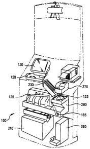
devices and purposes. One device is illustrated in Fig 1A. In this device,
coins are placed into a tray 120, and
fed to a sensor region 123 via a first ramp 230 and coin pickup assembly 280.
In the sensor region 123, data
is collected by which coins are discriminated from non-coin objects, and
different denominations or countries
of coins are discriminated. The data collected in the sensor area 123 is used
by the computer at 290 to control
movement of coins along a second ramp 125 in such a way as to route the coins
into one of a plurality of bins
210. The computer may output information such as the total value of the coins
placed into the tray, via a
printer 270, screen 130, or the like. In the depicted embodiment, the
conveyance apparatus 230,280 which
is upstream of the sensor region 123 provides the coins to the sensor area 123
serially, one at a time.
The embodiment depicted in Fig 1B generally includes a coin counting/sorting
portion 12 and a
coupon/voucher dispensing portions 14a,b. In the depicted embodiment, the coin
counting portion 12 includes
an input tray 16, a voucher dispensing region 18, a coin return region 22, and
customer I/O devices, including
a keyboard 24, additional keys 26, a speaker 28 and a video screen 32. The
apparatus can include various
indicia, signs, displays, advertisement and the like on its external surfaces.
A power cord 34 provides power
to the mechanism as described below.
Preferably, when the doom 36a, 36b are in the open position as shown, most or
all of the components
are accessible for cleaning and/or maintenance. In the depicted embodiment, a
voucher printer 23 (Fig. 41)
CA 02581740 2010-03-15
9
is mounted on the inside of the door 36a. A number of printers can be used for
this purpose. In one
embodiment, a model KLDS0503 printer, available from Axioh is used. The right-
hand portico of the cabinet
includes the coupon feeder 42 for dispensing. e.g., pro-printed manufacturer
coupon sheets through a chute
44 to a coupon hopper on the outside portion of the door 36b. A coomuter.46.
in the depicted anbixiiment,
is positioned at the top of the right hand portion of the cabinet in order to
provide a relatively clean, location
for the computer. An 1/0 board 481s positioned adjacent the sheet feeder 42.
The general coin path Gir the anbodimert depicted in Fig 1 is from the input
tray 16, down first sod
second chutes to a trammel 52, to a coin pickup assembly 54, along a coin rail
56 arid past a sensor 58 If.
based on sensor data, it is determined that the coin can and should be
accepted, a controllable deflector door
62 is activated to divot coins from their gravitational path to coin tubes
64a, b for delivery to coin trolleys 66s.
b. If it has not been determined that a coin can and should be accepted, the
door 62 is not activated and coins
(or other objects) continue down their gravitational or default path to a
reject chute 68 for delivery to a
customer-aocessible reject or return box 22.
Devices that may be used in connection with the input tray are described in
U.S. S.N. 08/255.539.
now U.S. Patent 5564546, 08/237,486, now U.S. Nicol 5620079, supra.
Devices that may be used in connection with the coin trolleys 66a, 66b are
described in &N.
08/883,776, fOf COIN BIN WITH LOCKING LID, now US Patent 6,082,519
Devices that may be used in connection with the coin chutes and the trail:um!
52 are described in
1'CT/US97/03136 Feb 28, 1997 published as WO 97/33257
In one embodiment, depicted in Figs. SI and 53, the trammel cage 5112 is
configured to facilitate removal, e.g. for cleaning or maintenance purposes or
the like. In the embodiment
depicted in rip 48.54, trommel removal can be accomplished with only one hand,
particularly by pressing
button 5212 (Fip 52 and 54)whids moves socket 5414 (Fig F4) out of atpgement
with crane pin 5414 (Fig
54) permitting the cradle 5416 which bears the trammel cage (as shown in Fig.
53) to pivot downward 5312
(Fig 53) from the position 4812 shown in Fig 48 to the position 4912 sham ia
Fig. 49. The cradle 5416
includes a telescoping section 5418a,b for permitting the treacle' cage to be
anther retracted to the position
5012 shown in fig 50 where it can be easily lifted from the cradle.
Briefly, and as described mom thoroughly below and in the above-noted
applications, a user is
provided with instructions such as on computer screen 32. The user places a
mass of coins, typically of a
phrality of dominations (typically scommortied by dirt or other non-coin
objects and/or foreign or otherwise
non-acceptable coins) in the input tray 16. The user is prompted to push a
button to inform the machine that
the user wishes to have coins discriminated Thereupon, the computer causes an
input gate 17 (Fig. 41) to
open and illuminates a signal to prompt the use- to begin feeding coins The
gate may be controlled to open
or close for a number of purposes, such as in respcsise to sensing of a jam,
sensing of load in the trommel or
coin pickup assembly, sod the like. In one embodiment, signal devices such as
LEDs can provide a user with
an indication of whether the gate is open or closed (or otherwise to prompt
the user to feed or discontinue
feeding coins cr ofixr rejects). Althcugh instructions to feed or divelotitub-
may be provided on the computer
=eat 32, indicator lights (although involving additional wiring and attendant
difficulties) re believed useful
CA 02581740 2007-03-29
10
since users often are watching the throat of the chute, rather than the
computer screen, during the feeding of
coins or other objects When the gate is open, a motor 19 (Fig. 41) is
activated to begin rotating the trommel
assembly 52. The user moves coins over the peaked output edge 72 of the input
tray 16, typically by lifting
or pivoting the tray by handle 74, and/or manually feeding coins over the peak
72. The coins pass the gate
(typically set to prevent passage of more than a predetermined number of
stacked coins, such as by defining
an opening equal to about 3.5 times a typical coin thickness). Instructions on
the screen 32 may be used to tell
the user to continue or discontinue feeding coins, can relay the status of the
machine, the amount counted thus
far, provide encouragement or advertising messages and the like.
First and second chutes (not shown in Fig. IB) are positioned between the
output edge 72 of the input
tray 16 and the input to the tontine( 52. Preferably, the second chute
provides a funneling effect by having
a greater width at its upstream edge than its downstream edge. Preferably, the
coins cascade or "waterfall"
when passing from the first chute to the second chute, e.g. to increase
momentum and tumbling of the coins.
Preferably, some or all of the surfaces that contact the coin along the coin
path, including the chutes,
have no fiat region large enough far a coin to contact the surface over all or
substantially all of one of the faces
of the coin. Some such surfaces are curved to achieve this result, such that
coins make contact on, at most,
two points of such surfaces. Other surfaces may have depressions or
protrusions such as being provided with
dimples, quilting or other textures. Preferably, the surface of the second
chute is constructed such that it has
a finite radius of curvature along any plane normal to its longitudinal axis,
and preferably with such radii of
curvature increasing in the direction of coin flow.
In one emlwyliment, the chutes are formed from injected molded plastic such as
an acetal resin e.g.
Debit), available from E.L DuPont de Nemours & Co., or a polyamide polymer,
such as a nylon, and the hie.
Other materials that can be used for the chute include metals, ceramics,
fiberglass, reinforced materials,
epoxies, ceramic-coated or -reinforced materials and the like. The chutes may
contain devices for performing
additional functions such as stops or traps, e.g., for dealing with various
types of elongate objects.
The trammel 52, in the depicted embodiment is a perforated-wall, square cross-
section, rotatably
mounted container. Preferably, dimples protrude slightly into the interior
region of the trommel to avoid
adhesion and/or reduce friction between coins and the interior surface of the
trommel. The trommel is rotated I
about its longitudinal axis. Preferably, operation of the device is monitored,
such as by monitoring current
draw for the trommel motor using a current sensor 21. A sudden increase or
spike in current draw may be
considered indicative of an undesirable load and/or jam of the trammel. The
system may be configured in
various ways to respond to such a sensed jam such as by turning off the
trammel motor to stop attempted
trommel rotation and/or reversing the motor, or altering motor direction
periodically, to attempt to clear the
jam. In one embodiment, when a jam or undesirable load is sensed, coin feed is
stopped or discouraged, e.g.,
by closing the gate and/or illuminating a "stop feed" indicator. As the
trommel motor 19 rotates the trommel,
one or more vanes protruding into the interior of the trammel assist in
providing coin-lifting/free-fall and
moving the coins in a direction towards the output region. Objects smaller
than the smallest acceptable coin
(about 17.5 mm, in one embodiment) pass through the perforated wall as the
coins tumble. In one embodiment,
the holes have a diameter of about 0.61 inches (about 1.55 cm) to prevent
passage of U.S. dimes. An output
CA 02 5 8 17 4 0 2 0 10 - 0 3 - 15
11
chute directs the (at least partially) cleaned coins exiting the trammel
towards the coin pickup assembly 54.
The depicted hori2ontal disposition of the tronintel, which relies on vanes
rather than trammel inclination for
longitudinal coin movements, achieves a relatively small vertical space
requirement for the trammel.
Preferably the trammel is mowed in such a way that it may be easily removed
end/or opened or disassembled
for cleaning and maintenance, as described, e.g., iII rcr Application
US97/03I36. supra. ( WO 9 7 / 3 3 2 5 7 )
As depicted in Fig. 17, coin pickup assembly 54 includes a hopper 1702 for
receiving colas output
front the trammel 52. The hopper 1702 may be made at relatively low coat etch
as by vacuum forming. In
ale embodiment, the hopper 1702 is formed of. plastic material, =eh as
polyethylene. backed with sound-
absoibing foam for reducing noise. Preferably, the hopper (or other components
along the win path) are
configured to avoid slow-up, jams or other difficulties, such as may otherwise
result particularly from wet or
sticky coins. Without being bound by any than, it is believed that
polyethylene is useful to reduce coin
sticking. Thus, it may be desirable to include a mechanical or other
transducer for providing enemy, in
response to a sensed jam, abw-up or other abnormality. One ccofiguration for
providing energy is described
in U.S. patent 5,746,299 In one embodiment,
slow or stuck coins are
werinnirally provided with kinetic energy. Incise embodimait, vibrational or
other kinetic energy is imparted
by pulsing, alternating, reversing or otherwise activating the hopper motor.
Other features which may be
provided for Use hopper inch.* shaping to provide a curvature sufficient to
avoid face-to-face contact between
wins and the hopper surface ancVer providing surface texture (such as
embossing, dimpling, faceting, quilting,
ridging or ribbing) on the hopper interim. surface. The hopper 1702 preferably
has an amount of flexibility,
rather then being rigid, which reduces the occurrence of jams and assists in
clewing jams since coins are not
foroed against a actid, unyielding enlace.
As described below, the coin move into an annuli( coin path defined, on the
outside, by the edge of
a deader recess 1802 (Fig. 18) and, on the inside, by a ledge 1804 formed on a
rail disk 1806. The coins are
moved along the annular path by paddles 1704a, b, e, d for delivery to the
coin rail 56.
A circuit board 1744 for providing certain control functions, as described
below, is preferably
mewled mume gizerially accessible iced surface of the chassis 1864. An
electromagnetic interference (EMI)
safety thield 1746 normally covas the circuit board 1744 and swinp opat on
hinges 1748kb for euy service
SCOCIIIILIn the anbodiment depicted in Fig. 17 and IS, the coin rail 56 and
the recess 1808 for the disks am
formed as a single piece or block, such as the depicted base plate 1810. In
one embodiment, the base plate
1810 is formed from high density polyethylene (HDPE) and the recess 1808 and
coin nul 56, as well as the
various openings depicted, are formed by machining a sheet or block &HOPE. I-
IDPE is. useful material
because, among other reasons, components may be mounted using seffitapping
screws, reducing
manufactring cods. Furthermore, tine of. non-metallic back plate is prefared
in order to avoid interference
with the sensor. In one embodiment, electrically catchictive HOPE may be used,
e.g. to dissipate static
electricity.
The base plate 1810 is mounted co a chassis 1864 which is poaitioncd within
the cabinet (Fig. 1B)
suth that the base plate 1810 is disposed at an angle 1866 with respect to
vertical 1868 &between about 0'
CA 02581740 2007-03-29
12
and about 45 , preferably between about 0 and about 15 , more preferably
about 20 . Preferably, the diverter
cover 1811 is pivotally c.oupled to the baseplate 1810, e.g. by hinges 1872a,
1872b, so that the diverter cover
1811 may be easily pivoted forward (Fig. 19), e.g. for cleaning and
maintenance.
A mtating main disk 1812 is configured for tight (small clearance) fit against
the edge 1802 of recess
1808. Finger holes 1813a, b, c, d facilitate removal of the disk for cleaning
or maintenance. Relatively loose
(large clearance) fit is provided between disk holes 1814a, b, c, d and hub
pins 1816a, b, c, d and between
central opening 1818 and motor hub 1820. The loose fit of the holes and the
tight fit of the edge of dislc 1812
assist in reducing debris entrapment and motor jams. Because the main disk is
received in recess 1802, it is
free to flex and/or tilt, to some degree, e.g. in order to react to coin jams.
A stationary rail disk 1806 is positioned adjacent the main disk 1812 and has
a central opening 1824
fitting loosely with respect to the motor hub 1820. In one embodiment, the
rail disk is formed of graphite-filled
phenolic.
The ledge 1804 defined by the rail dislc 1806 is preferably configured so that
the annular coin path
flares or widens in the direction of coin travel such that spacing between the
ledge and the recess edge near
the bottom or beginning of the coin path (at the eight o'clock position 1876)
is smaller (such as about 0.25
inches, or about 6 mm smaller) than the corresponding distance 1827 at the
twelve o'clock position 1828. In
one embodiment, the rail disk 1806 (and motor 2032) are mounted at a slight
angle to the plane formed by the
attachment edge 2042 of the hopper 1702 such that, along the coin path, the
coin channel generally increases
in depth (i.e. in a direction perpendicular to the face of the rail disk).
As the coins travel counterclockwise from approximately a 12:00 position 1828
of the rail disk, the
ledge is thereafter substantially linear along a portion 1834 (Fig. 19)
extending to the periphery of the rail disk
1806 and ending adjacent the coin bacicplate 56 and rail tip 1836. A tab-like
protrusion 1838 is engaged by
rail tip 1836, holding the rail dislc 1806 in position. The rail disk is
believed to be more easily manufactured
and constructed than previous designs, such as those using a coin knife.
Furthermore, the present design
avoids the problem, often found with a coin knife, in which the tip of the
knife was susceptible to prying
outward by debris accumulated behind the tip of the coin knife.
A tension dislc 1838 is positioned adjacent the rail disk. The tension disk
1838 is mounted on the
motor hub 1820 via central opening 1842 and threaded disk knob 1844. As the
knob 1844 is tightened, spring
fingers 1846a, b, c, d apply force to keep the disks 1838, 1806, 1812 tightly
together, reducing spaces or
cracks in which debris could otherwise become entrapped. Preferably, the knob
1844 can be easily removed
by hand, pamitting removal of all the disks 1812, 1806, 1838 (e.g., for
maintenance or cleaning) without the
need for tools.
In one embodiment, the tension disk 1838 and main disk 1812 are formed of
stainless steel while the
rail disk 1806 is formed of a different material such as graphite-filled
phenolic, which is believed to be helpful
in reducing galling. The depicted coin disc configuration, using the described
materials, can be manufactured
relatively easily and inexpensively, compared to previous devices. Paddles
1704a, b, c, d are pivotally
mounted on tension disk pins 1848a, b, c, d so as to permit the paddles to
pivot in directions 1852a, 1852b
parallel to the tension disk plane 1838. Such pivoting is useful in reducing
the creation or exacerbation of coin
CA 02581740 2007-03-29
13
jams since coins cc other items which are stopped along the coin path will
cause the paddles to flex, or to pivot
around pins 1848a, b, c, d, rather than requiring the paddles to continue
applying full motor-induced force on
the stopped coins or other objects. Springs 1854a, b, c, d resist the pivoting
1852a, 1852b, urging the paddles
to a position oriented radially outward, in the absence of resistance e.g.
from a stopped coin or other object.
Preferably, sharp or irregular surfaces which may stop or entrap coins are
avoided. Thus, covers
1856a, b, c, d are placed over the springs 1854a, b, c, d and conically-shaped
washers 1858a, b, c, d protect
the pivot pins 1848a, b, c, d. In a sirnilar spirit, the edge of the tension
disk 1862 is angled or chamfered to
avoid coins hanging on a disk edge, potentially causing jamming.
As depicted in Fig. 25, a number of components are mounted on the rear surface
of the chassis 1864.
A motor, such as model 2032 drives the rotation of dislcs 1812, 1838 via motor
drive hub 1820. An actuator
such as solenoid 2014 controls movement of the trap door 1872 (described
below). A sensor assembly,
including sensor printed circuit board (PCB) 2512 is slidably mounted in a
shield 2514.
The lower edge of the recess 1808 is formed by a separate piece 1872 which is
mounted to act as a
trap door. The trap door 1872 is configured to be moved rearwardly 2012 (Fig.
20) by actuator 2014 to a
position 2016 to enable debris to fall into debris cup 2018. Solenoid 2014 is
actuated under control of a
microcontroller as described below. Preferably, the trap door 1872 retracts
substantially no further than the
front edge of the coin rail disk, to avoid catching, which could lead to a
failure of the trap door to close.
Preferably, a sensor switch provides a signal to the microcontroller
indicating whether the trap door has
completely shut Preferably the trap door is resiliently held in the closed
position in such a manner that it can
be manually opened if desired.
Coins which fall into the hopper 1702 from the trommel 52 are directed by the
curvature of the
hopper towards the 6:00 position 1877 (Fig. 19) of the annular coin path. In
general, coins traveling over the
downward-turning edge 2024 of the hopper 1702 are tipped onto edge and,
partially owing to the backward
inclination 1866 of the apparatus, tend to fall into the annular space 1801.
Coins which are not positioned in
the space 1801 with their faces adjacent the surface of the rail disk (such as
coins that may be tipped outward
2026a or may be perpendicular to the rail disk 2026b) will be struck by the
paddle 1704 as it rotates, agitating
the coins and eventually correctly positioning coins in the annular space 1801
with their faces adjacent the face
1801 of the annular space defined by the rail disk 1806. It is believed that
the shape of the paddle head 2028a,
2028c, in particular the rounded shape of the radially outmost portion 2206 of
the head, assists in agitating or
striking coins in such a manner that they will assume the desired position.
Once coins are positioned along the annular path, the leading edge of the
paddle heads 2028 contact
the trailing edge of the coins, forcing them along the coin path, e.g. as
depicted in Fig. 17. Preferably each
paddle can move a plurality of coins, such as up to about 10 coins. The coins
are thus eventually forced to
travel onto and along the linear portion 1834 of the rail disk ledge 1804 and
are pushed onto the coin rail tip
1836. Some previous devices were provided with an exit gate for coins exiting
the coin pickup assembly
which, in some cases, was susceptible to jamming. According to an embodiment
of the present invention, such
jamming is eliminated because no coin pickup assembly exit gate is provided.
CA 02581740 2007-03-29
14
As the paddle heads 2028 continue to move along the circular path, they
contact the linear portion
1834 (Fig. 19) of the ledge 1804 and flex axially outward 2032, facilitated by
a tapered shape of the radially
inward portion of the paddle pad 2028 to ride over (i.e. in front of) a
portion 1884 of the rail disk. In one
embodiment, openings or holes 1708 are provided in this portion to reduce
frictional drag and to receive e.g.
trapped debris, which is thus cleared from the annular coin path.
As seen in Fig. 21, the ledge 1804 as defined by the rail disk 1806 is
displaced upwardly 2102 with
respect to the ledge 2104 of the coin rail tip 1836. The distance 2102 may be,
for example, about 0.1 inches
(about 2.5 nun). The difference in height 2102 assists in gravitationally
moving coins from the rail disk ledge
1804 over the upper portion of the "V" gap (described below) and onto the
ledge of coin rail tip 1836.
The terminal point 2105 of the rail disk ledge is laterally spaced a distance
2107 from the initial edge
of the coin rail ledge 2104 to define a "V" gap therebetween. This gap, which
extends a certain distance 2109
circumferentially, as seen in Fig. 21, receives debris which may be swept
along by the coin paddles. The
existence of the gap 2107, and its placement, extending below the rail ledge,
by providing a place for debris
swept up by the paddles, avoids a problem found in certain previous devices in
which debris tended to
accumulate where a disk region met a linear region, sometimes accumulating to
the point of creating a bump
or obstruction which could cause coins to hop or fly off the ledge or rail.
The coin rail 56 functions to receive coins output by the coin pickup assembly
54, and transports the
coins in a singulated (one-at-a-time) fashion past the sensor 58 to the
diverting door 62. Singulation and
separation of coins is of particular use in connection with the described
sensor, although other types of sensors
may also benefit from coin singulation and spacing. In general, coins are
delivered to the coin rail 56 rolling
or sliding on their edge or rim along the rail ledge 2104. The face of the
coins as they slide or roll down the
coin rail are supported, during a portion of their travel, by rails or
stringers 2106a, b, c. The stringers are
positioned (Fig 23A), respectively, at heights 2108a, b, c (with respect to
the height of the ledge 2104) to
provide support suitable for the range of coin sizes to be handled while
providing a relatively small area or
region of contact between the coin face and the stringers. Although some
previous devices provide for flat-
topped or rounded-profile rails or ridges, the present invention provides
ridges or stringers which at least in
the second portion, 2121b, have a triangular or peaked profile. This is
believed to be easier to manufacture
(such as by machining into the baseplate 1810) and also maintains relatively
small area of contact with the coin
face despite stringer wear.
The position and shape of the stringers and the width of the rail 2104 are
selected depending on the
range of coin sizes to be handled by the device. In one embodiment, which is
able to handle U.S. coins in the
size range between a U.S. dime and a U.S. half-dollar, the ledge 2104 has a
depth 2111 (from the backplate
2114) of about 0.09 inches (about 2.3 mm). The top stringer 2106a is
positioned at a height 2108a (above
the ledge 2104), of about 0.825 inches (about 20 mm), (the middle stringer
2106b is positioned at a height
2108b of about 0.49 inches (about 12.4 mm), and the bottom stringer 2106c is
positioned at a height of about
0.175 inches (about 4.4 mm). In one embodiment, the stringers are about 0.8
inches (about 2 mm) wide 2109
(Fig. 23C) and protrude about 0.05 inches (about 1.3 mm) 2112 above the back
plate 2114 of the coin rail.
CA 02581740 2007-03-29
15
As seen in Fig. 22, as the coins enter the coin rail 56, the coins are
typically horizontally singulated,
i.e., coins are in single file, albeit possibly adjacent or touching one
another. The singulated configuration of
the coins can be contrasted with coins which are horizontally partially
overlapped 2202a,b as shown in Fig.
22A. Fig. 22A also illustrates a situation in which some coins are stacked on
top of one another vertically
2202c, d. A number of features of the coin rail 56 contribute to changing the
coins from the bunched
configuration to a singulated, and eventually separated, series of coins by
the time they move past the sensor
58. One such feature is a cut-out or recess 2116 provided in or adjacent the
top portion of the rail along a first
portion of its extent. As seen in Fig. 24, when coins which are vertically
stacked such as coins 2202c, b,
illustrated in Fig. 22, reach the cut-out portion 2116, the top coin, aided by
the inclination 1866 of the rail, tips
backward 2402 an amount sufficient that it will tend to slide forward 2404 in
front of the lower coin 2202,
falling into the hopper extension 2204 which is positioned beneath the cut-out
region 2116, and sliding back
into the main portion of the hopper 1702 to be conveyed back on to the coin
rail.
Another feature contributing to singulation is the change in inclination of
the coin rail from a first
portion 2121a which is inclined, with respect to a horizontal plane 2124 at an
angle 2126 of about 0 to about
30 , preferably about 0 to about 15 and more preferably about 100, to a
second portion 2121b which is
inclined with respect to a horizontal plane 2124 by an angle 2128 of about 300
to about 600, preferably
between about 400 and about 50 and more preferably about 45 . Preferably, the
coin path in the transitional
region 2121c between the first portion 2121a and second portion 2121b is
smoothly curved, as shown. Inane
embodiment, the radius of curvature of the ledge 2104 in the transition region
2121c is about 1.5 inch (about
3.8 cm).One feature of singulating coins, according to the depicted
embodiment, is to primarily use
gravitational forces for this purpose. Use of gravity force is believed to, in
general, reduce system cost and
complexity. This is accomplished by configuring the rail so that a given coin,
as it approaches and then enters
the second portion 2121b, will be gravitationally accelerated while the next
("followin() coin, on a shallower
slope, is being accelerated to a much smaller degree, thus allowing the first
coin to move away from the
following coin, creating a space therebetvieen and effectively producing a gap
between the singulated coins.
Thereafter, the following coin moves into the region where it is, in turn,
accelerated away from the successive
coin. As a coin moves from the first region 2121a toward and into the second
region 2121b, the change in rail
inclination 2126, 2318 (Fig. 21) causes the coin to accelerate, while the
following coins, which are still
positioned in the first region 2121a, have a relatively lower velocity.
In one embodiment, acceleration of a coin as it moves into the second rail
region 2121b is also
enhanced by placement of a short, relatively tall auxiliary stringer 2132
generally in the transition region
2121c. The auxiliary stringer 2132 projects outwardly from the back surface
2114 of the coin rail, a distance
2134 (Fig. 23B) greater than the distance 2112 of projection of the normal
stringers 2106a, b, c. Thus, as a
coin moves into the transition region 2121c, the auxiliary stringer 2132 tips
the coin top outward 2392, away
from contact with the normal stringers 2106a, b, c so that it tends to "fly"
(roll or slide on its edge or rim along
the coin rail ledge 2104 without contact with the normal stringers 2106a, b,
c) and, for at least a time period
following movement past the auxiliary stringer 2132, continues to contact the
coin rail only along the ledge
CA 02581740 2007-03-29
16
2104, further minimizing or reducing fiction and allowing the coin to
accelerate along the second region
2121b of the coin rail. In one embodiment the coin-contact portion of the
stringers in the first portion 2121a
are somewhat flattened (Fig. 23A) to increase friction and exaggerate the
difference in coin acceleration
between the first section 2121a and the second section 212th, where the
stringer profiles are more pointed,
such as being substantially peaked (Fig. 23C).
Mother feature of the coin rail contributing to acceleration is the provision
of one or more free-fall
regicos where coins will normally be out of contact with the stringers and
thus will contact, at most, only the
ledge portion 2104 of the rail. hi the depicted embodiment, a first free-fall
region is provided at the area 2136a
wherein the auxiliary stringer 2132 terminates. As noted above, coins in this
region will tend to contact the
coin rail only along the ledge 2104. Mother free-fall region occurs just
downstream of the upstream edge
2342 of the door 62. As seat in Fig. 23E, the door 62 is preferably positioned
a distance 2344 (such as about
0.02 inches ,about 0.5 mm) from the surface 2114 of the rail region. This
setback 2344, combined with the
termination of the stringers 2106, provides a free-fall region adjacent the
door 62. If desired, another free-fall
region can be provided downstream from the door 62, e.g., where the reject
coin path 1921 meets the
(preferably embossed) surface of the reject chute or reject chute entrance
which may be set back a distance
such as about 1/8 inch (about 3 mm).
Mother fine-fail region may be defined near the location 2103 where coins exit
the disks 1812, 1806
and aiter the rail 56, e.g., by positioning the disk 1812 to have its front
surface in a plane slightly forward (e.g.,
about 0.3 inches, or about 7.5 mm) of the plane defined by rail stringers
2106. This free-fall region is useful
not only to assist the transition from the disk onto the rail but makes it
more likely that coins which may be
slowed or stopped on the rail near the end of a transaction will be positioned
downstream of the retract position
(Fig. 21) of the rake 2152 such that when the rake operates (as described
below), it is more likely to push
slowed or stopped coins down the rail than to knock such coins off the rail.
Providing periods of coin flying
reduces fiction, contributes to coin acceleration and also reduces variation
in coin velocity since sticky or wet
coins behave similarly to pristine coins when both are in a flying mode.
Producing periods of flying is believed
to be particularly useful in maintaining a desired acceleration and velocity
of coins which may be wet or sticky.
The sensor 58 is positioned a distance 2304 (Fig. 23D) away from the surface
of the stringers 2106a,
b, c sufficient to accommodate passage of the thickest coin to be handled.
Although certain preferred sensors,
and their use, are described more thoroughly below, it is possible to use
features of the present invention with
other types of sensors which may be positioned in another fashion such as
embedded in the coin rail 56.
The leading surface of the sensor housing is preferably ramped 2306 such that
coins or other objects
which do not travel into the space 2304 (such as coins or other objects which
are too large or have moved
partially off the coin path) will be deflected by the ramp 2306 onto a bypass
chute 1722 (Fig. 17), having a
deflector plane 1724 and a trough 1726 for delivery to the coin return or
reject chute 68 where they may be
returned to the user. The sensor housing also performs a spacer function,
tending to hold any jams at least a
minimum distance from the sensor core, preferably sufficiently far that the
sensor reading is not affected (which
could cause misdetection). If desired, the sensor housing can be configured
such that jams may be permitted
within the sensing range of the sensor (e.g., to assist in detecting jam
occurrence).
CA 02581740 2007-03-29
17
In the depicted configuration, the sensor 58 is configured so that it can be
moved to a position 2142
away from the coin rail 56, for cleaning or maintenance, such as by sliding
along slot 2144. Preferably, the
device is constructed with an interference fit so that the sensor 58 may be
moved out of position only when the
diverter cover 1811 has been pivoted forward 1902 (Fig. 19) and such that the
diverter cover 1811 may not
be repositioned 1904 to its operating configuration until the sensor 2142 has
been properly positioned in its
operating location (Fig 21). In another embodiment, depicted in Figs 43 - 47,
closing the diverter cover 1811
before the sensor 2142 has been properly positioned, is prevented by
interference with a pin 4312 (rather than
interference with the sensor itself, which could result in impact and/or
damage to the sensor). In the depicted
embodiment, the pin 4312 is registered with a hole 4313 in the diverter cover
1811 when the sensor 2412 is
in the unretracted position shown in Fig. 43. Fig 44 shows the configuration
with the diverter cover 1811
open. With the diverter cover 1811 in the open position, the sensor 2142 can
be moved from the unretracted
position (Figs 43,44) to the retracted position (Fig 46), eg. For purposes of
cleaning, maintenance and the Isle.
Fig. 45 is a rear view showing the bottom edge 4511 of the sensor assembly
protruding from under a sensor
cover 4512. In the depicted embodiment, when the sensor is refracted the
bottom edge 4511 moves from the
position shown in fig 45 to the position shown in fig 47. (Although Fig 47
shows the cover 4512 moving with
the sensor, it is also possible to configure the cover 4512 to be stationary
while the sensor 2142 is retracted.)
To avoid accidentally leaving the sensor in the retracted position when the
cleaning and maintenance
operations are completed, as the sensor is retracted, the bottom edge 4511
moves a pin 4515, projecting
rearwardly from a rotatably-mounted disk 4517. Movement of the pin 4515 causes
the disk 4517 to rotate
4519, against the urging of spring 4521, carrying the pin 4312 to the position
shown in fig 46, out of
registration with the hole 4313. When thus moved, the pin 4312 is positioned
such that, if an attempt is made
to close 4612 the diverter cover 1811 while the sensor is retracted (Fig. 46)
the rear surface of the diverter
cover 1811 will strike the pin 4312, preventing closure of the cover 1811. By
sliding the sensor to its
unretracted position (Fig. 44) the spring 4521 rotates the disk 4517 to return
the pin 4312 to the position
depicted in Fig. 44, registered with the hole 4313, permitting closure of the
cover 1811. Preferably, the sensor
apparatus is configured so that it will seat reliably and accurately in a
desired position with respect to the coin
rail such as by engagement of a retention clip 2704 (Fig. 21). Such seating,
preferably combined with a
relatively high tolerance for positional variations of coins with respect to
the sensor (described below), means
that the sensor may be moved to the maintenance position 2142 and returned to
the operating position
repeatedly, without requiring recalibration of the device.
As noted above, in the depicted embodiment, a door 62 is used to selectively
deflect coins or other
objects so the coins ultimately travel to either an acceptable-object or coin
bin or trolley, or a reject chute 68.
In the embodiment depicted in Fig. 43, a coin return ramp 4312 extends from
the coin return region
1921, through the opening 1813 of the diverter cover 1811 and extends a
distance 4314 outward and above
the initial portion of the coin return chute 68. Thus, coins which are not
deflected by the door 62 travel down
the ramp 4312 and fly off the end 4316 of the ramp in a "ski jump" fashion
before landing on the coin return
chute surface 68. Even though preferably, coin contact =faces such as the ramp
4312 and coin return chute
68 are embossed or otherwise reduce facial contact with coins, providing the
"ski jump" flying region further
CA 02581740 2007-03-29
18
reduces potential for slowing or adhesion of coins (or other objects) as they
travel down the return chute
towards the customer return box.
Preferably the device is configured such that activation of the door deflects
coins to an acceptable coin
bin and non-activation allows a coin to move along a default path to the
reject chute 68. Such "actuate-to-
accept" technique not only avoids accumulation of debris in the exit bins but
improves accuracy by accepting
only coins that are recognized and, further, provides a configuration which is
believed superior during power
failure situations. The actuate-to-accept approach also has the advantage that
the actuation mechanism will
be operating on an object of known characteristics (e.g. known diameter, which
may be used, e.g. in connection
with determining velocity and/or acceleration, or known mass, which may be
used, e.g for adjustment of
forces, such as deflection forces). This affords the opportunity to adjust,
e.g. the timing duration and/or
strength of the deflection to the speed and/or mass of the coin. In a system
in which items to be rejected are
actively deflected, it would be necessary to actuate the deflection mechanism
with respect to an object which
may be unrecognized or have unknown characteristics.
Although in one embodiment the door 62 is separately actuated for each
acceptable coin (thus
reducing solenoid 2306 duty cycle and heat generation), it would also be
possible to configure a device in
which, when there are one or two or more sequential accepted coins, the door
62 is maintained in its flexed
position continuously until the next non-accepted coin (or other object)
approaches the door 62.
An embodiment for control and timing of the door 62 deflection will be
described more thoroughly
below. In the depicted embodiment, the door 62 is deflected by activation of a
solenoid 2306. The door 62,
in one embodiment, is made of a hard resilient material, such as 301 full hard
stainless steel which may be
provided in a channel shape as shown. In one embodiment, the back surface of
the coin-contact region of the
door 2308a is substantially covered with a sound-deadening material 2334 such
as a foam tape (available from
3M Ccenpany). PreSrrably the foam tape has a hole 2335 adjacent the region
where the solenoid 2306 strikes
the door 62.
In one embodiment, the door 62 is not hinged but moves outwardly from its rest
position (Fig. 23E)
to its deflected position (Fig. 23F) by bending or flexing, rather than
pivoting Door 62, being formed of a
resilient material, will then deflect back 2312 to its rest position once the
solenoid 2306 is no longer activated.
By relying on resiliency of an unhinged door for a return motion, there is no
need to provide a door return
spring. Furthermore, the resiliency of the door, in general, provides a force
greater than the solenoid spring
return force normally provided with a solenoid, so that the door 62 will force
the solenoid back to its rest
position (Fig. 23E) (after cessation of the activation pulse), more quickly
than would have been possible if
relying only on the force of the solenoid return spring As a result, the
effective cycle time for the solenoid/door
system is reduced. In one embodiment, a solenoid is used which has a normal
cycle time of about 24
millismciwis but which is able to achieve a cycle time of about 10
milliseconds when the resilient-door-closing
feature is used for solenoid return, as described. In one embodiment, a
solenoid is used which is rated at 12
volts but is activated using a 24-volt pulse.
In some situations, particularly at the end of a coin discrimination cycle or
transaction, one or more
coins, especially wet or sticky coins, may reside on the first portion 2121a
of the rail such that they will not
CA 02581740 2007-03-29
19
spontaneously (or will only slowly) move toward the sensor 58. Thus, it may be
desirable to include a
mechanical or other transducer for providing energy, in response to a sensed
jam, slow-up or other
abnormality. One configuration for providing energy is described in U.S.
patent 5,746,299, incorporated
herein by reference. According to one anbodiment for providing energy, a coin
rake 2152, normally refracted
into a rake slot 2154 (Fig. 23A), may be activated to extend outward 2156 from
the slot 2154 and move
lengthwise 2156 down the slot 2154 to push slow or stopped coins down the coin
path, such as onto the second
portion 2121b of the coin rail, or off the rail to be captured by the hopper
extension 2204. An embodiment
for timing and control of the rake is described more thoroughly below. In one
embodiment, rake movement
is achieved by activating a rake motor 2502 (Fig. 19) coupled to a fink arm
2504 (Fig. 25). This link 2504
is movably mounted to the rear portion of the chassis 1864 by a pin and slot
system 2506a,b, 2507a,b. A plate
section 2509 of the Fmk 2504 is coupled via slot 2511 to an eccentric pin of
motor 2502. A slot 2513 of the
link arm 2504 engages a rear portion of the rake 2152. Activation of the motor
2502 rotates eccentric pin
2515 and causes link 2504 to move longitudinally 2517. A slot 2513 of the link
arm 2504, forces the rake
2152 to move 2519 along the inclined slot 2154 toward a downstream position
2510 ( Fig. 26A). The function
of causing the rake to protrude or extend outward 2156 from the slot 2154 can
be achieved in a number of
fashions. In one embodiment, the link arm 2504 is shaped so that when the rake
is positioned down the slot
2154, the rake 2152 is urged outwardly 2156 bu the shape of the resilient link
arm 2504. As the rake is moved
upstream 2525 toward the normal operating location, a cam follower formed on
the free end 2527 of the link
ann is urged reanvardly by a cam 2529 carrying the rake 2152 with it,
rearwardly to the retracted position (Fig.
23A, Fig. 26).
Preferably, the rake position is sensed or monitored, such as by sensing the
position of the rake motor
2502, in order to ensure proper rake operation. Preferably the system will
detect (e.g. via activity sensor 1754)
if the coin rake knocked coins off the rail or, via coin sensor 58,11 the coin
rake pushed coins down the coin
rail to move past the sensor 58. In one embodiment if activation of the coin
rake results in coins being knocked
off the rail or moved down the rail, the coin rake will be activated at least
a second time and the system may
be configured to output a message indicating that the system should be cleaned
or requires maintenance.
Between the time that a coin passes beneath the sensor 58 and the time it
reaches the deflection door
62 (typically a period of about 30 milliseconds), control apparatus and
software (described below) determine
whether the coin should be diverted by the door 62. In general, it is
preferred to make the time delay between
sensing an object and deflecting the object (i.e., to make the distance
between the sensor and the deflection
door) as short as possible while still allowing sufficient time for the
recognition and categorization processes
to operate. The time requirements will be at least partially dependent on the
speed of the processor which is
used. In general, it is possible to shorten the delay by employing a higher-
speed processor, albeit at increased
expense. Shortening the path between the sensor and the deflector not only
reduces the physical size of the
device but also reduces the possibility that a coin or other object may become
stuck or stray from the coin path
after detection and before disposition (potentially resulting in errors, e.g.
of a type in a coin is "credited" but
not directed to a coin bin). Furthermore, shortening the separation reduces
the chance that a faster following
coin will "catch up" with a previous slow or sticky coin between the sensor
and the deflector door. Shortening
CA 02581740 2007-03-29
20
the separation additionally reduces the opportunity for coin acceleration or
velocity to change to a significant
degree between the sensor 58 and the door 62. Since the door, in one
embodiment, is controlled based on
velocity or acceleration measured or (calculated using data measured) at the
sensor, a larger separation (and
consequently larger rail length with potential variations is, e.g. fiction)
between the sensor 58 and the door
62 increases the potential for the measured or calculated coin velocity or
acceleration to be in error (or
misleading).
Because the coin deflector requires a certain minimum cycle time (i.e., the
time from activation of
the solenoid until the door has returned to a rest state and is capable of
being reactivated), it is impossible to
successfully deflect two coins which are too close together. Accordingly, when
the system determines that two
coins are too close together (e.g. by detecting successive "trail" times which
are less than a minimum period
apart), the system will refrain from activating the deflector door upon
passage of one or both such coins, thus
allowing one or bodi such coins to follow the default path to the reject
chute, despite the fact that the coins may
have been both successfully recognized as acceptable coins.
If a coin is to be diverted, when it reaches the door 62, solenoid 2306 is
activated. Typically, because
of the step 2136b and/or other flying-inducing features, by the time a coin
reaches door 62 it will be spaced
a short distance 2307 (such as 0.08 inches, or about 2 mm) above the door
plane 62 and the door, as it is
deflected to its activated position (Fig. 23F), will meet the flying coin and
knock the coin in an outward
direction 2323 to the common entrance 1728 of acceptable-coin tubes 64a, 64b.
Preferably all coin contact
surfaces of the return chute and coin tube are provided with a surface texture
such as an embossed surface
which will reduce friction and/or adhesion. Additionally, such surfaces may be
provided with a sound-
deadening material and/or a kinetic energy-absorbing material (to help direct
coins accurately into the accept
bins).
In one embodiment, the timing of deflection of the door 62 is controlled to
increase the likelihood that
the door will strike the coin as desired in such a fashion as to divert it to
entrance to the coin tubes 1728. The
preferred striking position may be selected empirically, if desired, and may
depend, at least partially, on the
diameter and mass of the coins and the coin mix expected in the machine as
well as the size and characteristics
of the door 62. In one embodiment, the machine is configured to, on average,
strike the coin when the leading
edge of the coin is approximately 3 mm upstream ("upstream" indicating a
direction opposite the direction of
coin flow 2332) of the downstream edge 2334 of the actuator door 62 (Fig.
23E). In one embodiment, this
strike position is the preferred position regardless of the diameter of the
coin.
Preferably, there is a gap between coins as they stream past the door 62. The
preferred gap between
adjacent coins which have different destinations (i.e., when adjacent coins
include an accepted coin and a not-
accepted coin) depends on whether the accepted coin is before or after the non-
accepted coin (in which the
"accepted coin" is a coin which will be diverted by the door and the not-
accepted coin will travel past the door
without being diverted). The gap behind a not-accepted coin (or other object)
which reaches the door 62
before an accepted coin is referred to herein as aleading gap". The gap behind
an accepted coin is referred
to herein as a "trailing gap". In one embodiment, the preferred leading gap is
described by the following
equation:
GAP,õõ,,..õ, = ildss.õ.õ4, + Errorph. + a (1)
CA 02581740 2007-03-29
21
where:
Ad.," represents the change in the actual inter-coin gap from the time the
coins pass the sensor
58 to the time when the coins reach the door 62 (approximately 3 nun);
Error.. represents the distance error due to compensation uncertainties,
assuming leading gap
worst conditions of maximum initial velocity and a frictionless rail
(approximately 6 mm);
and
a represents the dimension from the downstream edge of the actuator door
2334 to the
leading edge of the coin at the preferred strike position (approximately 3
mm).
The preferred minimtnn leading gap of approximately 12 nun applies when a non-
accepted coin (or
other object) precedes an accepted coin. In the common case of a string of
consecutive accepted coins, this
constraint need not be enforced after the first coin in the stream.
In one embodiment, the preferred trailing gap is described by the following
equation:
GAP t = Adsõ,d + Ad, + Error, = + b - a - D = = (2)
where:
repicseauts the change in actual inter-coin gap between the sensor 58 and the
door 62
(approximately 2 mm);
Ad = represents the distance the coins travel during the time the actuator
door is extended
(approximately 5 mm);
Error,. represents the error due to compensation uncertainties, assuming
trailing gap worst
conditions of zero initial velocity and a sticky or high-friction rail
(approximately 6 mm);
represents the length 2336 of the door 62; and
D..represents the diameter of the accepted coin (in the worst case for a
common U.S. coin mix,
17.5 mm).
This results in a preferred minimum trailing gap of 5.2 ram.
A process for verifying the existence of preferred leading and trailing gaps,
in appropriate situations,
and/or selecting or controlling the activation of the door 62 to strike coins
at the preferred position, is described
below.
In the depicted embodiment, the region of the common entrance 1728 (Fig. 17)
is provided with a
flapper movable from a first position 1732a which guides the coins into the
first coin tube 64a for delivery,
ultimately, to a first coin trolley 66a, to a second position 1732b for
deflection to the second coin tube 64b for
delivery to the second coin trolley 66b. In one embodiment, the flapper 1732
is made of plastic to reduce noise
and the tendency to bind during operation. A solenoid actuator 1734, via link
arm 1736, is used to move the
flapper between the positions 1732a, 1732b, e.g. in response to control
signals from a microcontroller
(described below). The flapper 1732 may also be rapidly cycled between its
extreme positions to self-clean
material from the mechanism. In one embodiment, such self-cleaning is
performed after each transaction. In
one embodiment, coin detectors such as paired LEDs and optical detectors
1738a, b output signals to the
tnicrocontroller whenever passage of a coin is detected. These signals may be
used for various purposes such
as verifying that a coin deflected by the door 62 is delivered to a coin tube,
verifying that the flapper 1732 is
CA 02581740 2007-03-29
22
in the correct position, and detecting coin tube blockages such as may result
from backup of coins from an
over-filled coin bin. Thus, the sensor 1738a, 1738b at the end of each tube,
each provides data used for
performing two or more functions, such as verifying accepted-coin delivery,
verifying flapper placement and
verifying and detecting coin bin overfill.
As best seen in Figs. 27A and 27B, the sensor 58 is preferably directly
mounted on the sensor PCB
2512 and communicates, electrically, therewith via a header 2702 with leads
2704 soldered onto the board
2512. Providing the sensor and the sensor board as a single integrated unit
reduces manufacturing costs and
eliminates cabling and associated signal noise. The sensor 58 is made of a
core 2802 (Figs. 28A, 28B) with
a low-frequency 2804 and high frequency 2806 windings on the core. Polarity of
the windings should be
observed so that they are properly synchronized. Providing a winding in a
reverse direction can cause signal
cancellation.
The core 2802, in the depicted embodiment is generally U-shaped with a lower
annular,
semicircular, rectangular cross-sectioned portion 2808 and an upper portion
defining two spaced-apart legs
2812a, 2812b. The core 2802, in the depicted embodiment, has a thickness 2814
of less than about 0.5 inches,
preferably about 0.2 inches (about 5 mm), a height 2816 of about 2.09 inches
(about 53 mm) and a width
2818 of about 1.44 inches (about 3.65 cm) although other dimensions can also
be used, such as a thickness
greater than about 0.5 inches.
Because the sensor 58 is preferably relatively thin, 2814, the magnetic field
is relatively tightly
focused in the longitudinal (streamwise) direction As a result the coin or
other object must be relatively close
to the sensor before the coin will have significant effect on sensor output
For this reason, it is possible to
provide relatively close spacing of coins without substantial risk of
undesirable influence of a leading or
following coin on sensor output
The facing surfaces 2822a, b of the legs 2812a, b are, in the depicted
embodiment substantially
parallel and planar and are spaced apart a distance 2824 of about 0.3 inches
(about 8 mm). The interior facing
surfaces 2822a, b have a height at least equal to the width of the coin rail
2826, such as about 1.3 inches (about
33 mm). With the sensor positioned as depicted in Fig. 21 in the operating
configuration, the upper leg 2812a
of the core is spaced from the lower leg 2812b of the core (see Fig. 23D) by
the inter-face gap 2824 to define
a space 2304 for coin passage through the inter-leg gap. The core 2802 may be
viewed as having the shape
of a gapped tormid with extended legs 2812a, 2812b with parallel faces 2822a,
b. In one embodiment the
legs 2812a,b are substantially parallel. In another embodiment the legs
2812a,b are slightly inclined with
respect to one another to define a tapered gap. Without wishing to be bound by
any theory, it is believed that,
as depicted in Fig. 28E, extended faces which are inclined to define a gap
which slightly tapers 2832 (taper
exaggerated, for at least some embodiments in Fig. 28E) vertically downward
yields somewhat greater
sensitivity near the rail (where the majority of the coins or other items will
be located) but is relatively
insensitive to the vertical 2828 or horizontal 2832 position of coins therein
(so as to provide useful data
regardless of moderate coin bounce and/or wobble) as a coin passes through the
gap 2824. In the embodiment
of Fig. 28F, the extended faces taper in the opposite vertical direction 2834.
The faces may be configured at
an angle 2836a,b,c to the lateral axis 2838 of the sensor, as depicted in
Figs. 280, H, and I. By selecting the
CA 02581740 2007-03-29
23
angle(s) 2836 ABC used, or otherwise selecting the shapes of the sensor faces,
other tapered spaces between
the legs can be provided. It is also possible to provide for changes in inter-
leg spacing as a function of the
distance along the longitudinal axis 2858 including changes which are non-
linear, such as providing curved,
angled, dog-legged or similar sensor face configurations.
In the depicted embodiment, the faces 2822a,b extend 2816 across the entire
path width 2133, to
sense all metallic objects that move along the path in the region of the
sensor. It is also possible to provide
face extents which are larger or smaller than the path width, such as equal to
the diameter of the largest
acceptable coin.
It is believed that providing a core with a larger gap (i.e. with more air
volume) is partially
responsible for decreasing the sensitivity to coin misalignments but tends to
result in a somewhat lower
magnetic sensitivity and an increase in cross-talk. In one embodiment the
sensor can provide reliable sensor
output despite a vertical displacement ("bounce") of about 0.1 inch (about 2.5
mm) or more, and a sideways
(away from the stringers) displacement or "wobble" of up to 0.015 inches
(about 0.4 mm).
In the depicted embodiment the low frequency winding 2804 is positioned at the
bottom of the
semicircular portion 2808 and the high frequency winding is positioned on each
leg 2806a, b of the
semicircular portion. In one embodiment the low frequency winding is
configured to have an inductance (in
the driving and detection circuitry described below) of about 4.0 millihemys
and the high frequency winding
2806a, b to have an inductance of about 40 microhemys. These inductance values
are measured in the low
frequency winding with the high frequency winding open and measured in the
high frequency winding with
the low frequency winding shorted together. The signals on the windings are
provided to printed circuit board
via leads 2704.
In the embodiment of Fig. 28C, the low frequency winding 2842 crosses over
itself whereas in the
embodiment of Fig. MD, a single continuous winding 2844 is provided without
cross-over or multiple layers,
which is believed to improve the consistency and repeatability of sensor
performance. Without wishing to be
bound by any theory, this is believed to be due at least partially to
increasing the self-resonant frequency of the
low-frequency winding.
In the embodiment of Fig. 28C, the high frequency windings 2846 are positioned
about midway up
the bight 2846 of the sensor. In the embodiment of Fig. 28D, the high
frequency windings 2852 are positioned
farther towards the gapped end 2854 and, in the depicted embodiment, at a non-
orthogonal angle 2856 with
respect to the longitudinal axis 2858 of the sensor. The position of the high
frequency winding shown in Fig.
28D is believed to provide improved coupling from the high frequency windings
to the coin and less
undesirable coupling between the high frequency and the low frequency
windings. Further, it is believed that
by decreasing the number of turns for the high frequency winding, a resultant
decrease in the winding-to-coin
leakage inductance improves coin coupling (while maintaining the high
frequency winding inductance, as
described above) and further improves high frequency performance of the
sensor.
In addition to the toroid or torus-shaped sensors (Figs 2A, 2B), extended-leg
sensors (Figs. 28A-I)
and other depicted and described sensor shapes, other shapes for the magnetic
core can be provided, such as
a G-shape(5612, Fig. 56A), a C-shape (5614, Fig 56B), a triangular shape
(5618, Fig 56D), a square shape
CA 02581740 2007-03-29
24
(5616, Fig. 56C), a rectangular shape(5622, Fig 56E), a polygonal shape(5624,
Fig 56F), a circular shape
(214, Fig 2A), a V-shape (5626 Fig 56G), and an oval or elliptical shape(5628,
Fig. 56H, sections or portions
thereof and the like. It is believed that alternative magnetic core shapes can
be advantageously considered,
despite effects such shape changes may have on sensor performance, at least
partially because other shapes
may be found to be more cost-effective to produce.
Although the depicted embodiments provide a sensor with a single magnetic core
as a unitary piece,
it is possible to configure a sensor with two spaced apart components such as
providing the signal-generating
magnetic means on one side of a coin and a signal-receiving magnetic means on
the other side of a coin (as
the coin moves past the center). It is believed, however, that such a
multipart sensor will present alignment
requirements and may prove to be relatively expensive or provide less uniform
or reliable performance.
Fig 29 depicts the major functional components of the sensor PCB 2512. In
general, the sensor or
transducer 58 provides a portion of a phase locked loop which is maintained at
a substantially constant
frequency. Thus, the low frequency coil leads are provided to a low frequency
PLL 2902a and the high
frequency leads are provided to high frequency sensor PLL 2902b.
Fig. 40 provides an overview of a typical transaction. The transaction begins
when a user presses
a "go" or start button 4012. In response, the system opens the gate, and
begins the trammel and coin pickup
assembly disk motors 4014. As coins begin passing through the system, a sensor
(not shown) is used to
detennine if the hopper is in an overfill condition, in which case the gate is
closed 4018. The system is
continuously monitored for current peaks in the motors 4022 e.g. using current
sensors 21,4121 (Fig. 41) 90
that corrective action such as reversing either or both of the motors for
dejamming purposes 4024 can be
implemented.
During normal counting operations, the system will sense that coins are
streaming past the sensor
4026. The system is able to determine 4028 whether coins are being sent to the
reject chute or the coin trolley.
In the latter case, the system proceeds normally if the sensor in the coin
tube outputs an intermittent or
flickering signaL However, if the coin tube sensor is stuck on or off,
indicating a jam upstream or downstream
(such as an overfilled bin), operations are suspended 4036.
In one embodiment, the flow of coins through the system is managed and/or
balanced As shown in
Fig. 41, coin flow can be managed by, e.g., controlling any or all of the
state of the gate 17, state or speed of
the trommel motor 19 and/or state or speed of the coin pickup assembly motor
2032 e.g. to optimize or
otherwise control the amount of coins residing in the trommel ancVor coin
pickup assembly. For example, if
a sensor 1754 indicates that the coin pickup assembly 54 has become full, the
microcontroller 3202 can turn
off the trammel to stop feeding the coin pickup assembly. In one embodiment, a
sensor 4112, coupled to or
adjacent the trommel 52, senses the amount (and/or type) of debris falling out
of the trommel during a
particular transaction or time period and, in response, the microcontroller
3202 causes the coin pickup
assembly motor 2032 to run in a different speed and/or movement pattern (e.g.
to accommodate a particularly
dirty batch of coins), possibly at the expense of a reduction in throughput.
CA 02581740 2007-03-29
25
When the coin sensor 58 (and associated circuitry and software) are used to
measure or calculate coin
speed, this information may be used not only to control the deflector door 62
as described herein, but to output
an indication of a need for maintenance. For =ample as coin speeds decrease, a
message (or series of
messages) to that effect may be sent to the host computer 46 so that it can
request preventive maintenance,
potentially thereby avoiding a jam that might halt a transaction.
Once the system senses that coins are no longer streaming past the sensor, if
desired a sensor may
be used to determine whether coins are present e.g. near the bottom of the
hopper 4042. If coins are still
present, the motors continue operating 4044 until coins are no longer detected
near the bottom of the hopper.
Once no more coins are detected near the bottom of the hopper 4046, the system
determines that the
transaction is complete. The system will then activate the coin rake, and, if
coins are sensed to move past the
coin sensor 58 or into the hopper, the counting cycle is preferably repeated.
Otherwise, the transaction will
be considaed finished 4028, and the system will cycle the trap door and output
e.g. a voucher of a type which
may be exchanged for goods, services or cash.
The coin sensor phase locked loop (PLL), which includes the sensor or
transducer 58, maintains a
constant frequency and responds to the presence of a coin in the gap 2824 by a
change in the oscillator signal
amplitude and a change in the PLL error voltage. The phase locked loop shown
in the depicted embodiment
requires no adjustments and typically settles in about 200 microseconds. The
system is self-starting and begins
oscillating and locks phase automatically. It is also possible to provide
frequencies or signals for application
to a sensor without using a phase lock. The winding signals (2 each for high
frequency and low frequency
channels) are conditioned 2904 as described below and sent to an analog-to-
digital (M)) converter 2906.
The AID converter sample; and digitizes the analog signals and passes the
information to the microcontroller
3202 (Fig. 32) on the Control Printed Circuit Board Assembly (PCBA) (described
below) for further
manipulation to identify coins.
Although in one embodiment the signal or signals provided to the sensor are
substantially sinusoidal,
it is also possible to use configurations in which non-sinusoidal signals are
provided to the sensor, such as
(filtered or unfiltered) substantially square wave, pulse, triangle, or
similar periodic signals. Such non-
sinusoidal signals, in addition to offering system cost savings, for some
configurations, also typically include
various haimanivi. A haimmic-rich signal, such as a square wave signal is
believed to be affected differently
for different coins, e.g., due to the interrelationships of the various
harmonics' phases and amplitudes. For
example, in one embodiment, as depicted in Fig. 55D, application of a square
wave voltage to a sensor winding
may result in a harmonic-rich current flowing through the sensor winding 4552.
The sensor current can be
analyzed as depicted 4552 or various components or bandwidths of the sensor
current can be separated, e.g.,
using filters 4554a,b,c for analysis by, e.g., a microprocessor 4556 as
described herein. In this way, it is
possible to use one signal applied to a sensor coil in connection with two or
more signal detecting means for
distinguishing one coin from another. If desired, each signal detecting means
can be used to provide
information on one aspect of a coin's electrical properties. Alternatively, it
is possible to obtain information
on different aspects of a coin's electrical properties by providing different
signals 4542a,b,c, applying different
CA 02581740 2007-03-29
26
wave forms, frequencies, and the like 4544a,b,c to a coin, for detection by
sensors 4546a,b,c as depicted in
Fig. 55C.
Although a phase locked loop (PLL) approach to providing one or more constant
frequencies is
depicted in Fig. 29, other approaches can be used for achieving a relationship
between a first and a second
frequency. For example, as depicted in Fig. 55A, if a first frequency is
provided 4512, a frequency divider
4514 can be used to provide a second frequency 4516 in a known and stable
relationship to the first frequency.
In the embodiment of Fig. 55B, if a first frequency is provided 4522, a second
frequency, 4524 may be
obtained by using a mixer 4526 to combine the first frequency 4522 with a
third frequency 4528, as will be
clear to those who have skill in the art after understanding the present
disclosure.
One approach provides a plurality of signals for distinguishing coin types
(e.g., a different signal
"tuned" for each anticipated or acceptable coin type. It is believed this
approach may provide relatively high
accuracy but may involve additional cost compared to providing a reduced
number of signals.
Returning to the configuration of Fig. 29, as a coin passes through the
transducer 58, the amplitude
of the PLL error voltage 2909 a,b (sometimes referred to herein as a "D"
signal) and the amplitude of the PLL
sinusoidal oscillator signal (sometimes referred to as a "Q" signal) decrease.
The PLL error voltage is filtered
and conditioned for conversion to digital data. The oscillator signal is
filtered, demodulated, then conditioned
for conversion to digital data. Since three signals are generated by two PLL
circuits (high and low frequency),
four signals result as the "signature" for idmtifying coins. Two of the
signals (LF-D, LF-Q) are indicative of
low-frequency, coin characteristics, and the remaining two signals (HF-D, HF-
Q) are indicative of high-
frequency coin characteristics. Figure 30 shows a four channel oscilloscope
plot of the change in the four
signals (LF-D 3002, LF-Q 3004, HF-D 3006, and HF-Q 3008) as a coin passes the
sensor. Information about
the coin is represented in the shape, timing and amplitude of the signal
changes in the four signals. The
Control PCBA, which receives a digitized data representation of these signals,
performs a discrimination
algorithm to categorize a coin and determine its speed through the transducer,
as described below.
The coin sensor phase locked loop, according to one embodiment, consists of a
voltage controlled
oscillator, a phase comparator, amplifier/filter for the phase comparator
output, and a reference clock The
two PLL's operate at 200 ICHz and 2.0 MHZ with their reference clocks
synchronized. The phase relationship
between the two clock signals 3101a, b is maintained by using a divided-down
clock rather than two
independent clock sources 3102. The 2 MHZ clock output 3101a is also used as
the master clock for the M)
converter 2906.
As a coin passes through the transducer's slot, there is a change in the
magnetic circuit's reluctance.
This is seen by circuitry as a decrease in the inductance value and results in
a corresponding decrease in the
amplitude of the PLL error voltage, providing a first coin-identifying factor.
The passing coin also causes a
decrease in the amplitude of the sinusoidal oscillator waveform, depending on
its composition, e.g. due to an
eddy current loss, and this is measured to provide a second coin-identifying
factor.
The topology of the oscillators 2902a, b relies on a 180 degree phase shift
for feedback to its drive
circuitry and is classified as a Colpitts oscillator. The Colpitts oscillator
is a symmetric topology and allows
the oscillator to be isolated from ground. Drive for the oscillator is
provided by a high speed comparator
CA 02581740 2007-03-29
27
3104a, b. The canpwator has a fast propagation to minimize distortion due to
phase delay, low input current
to minimize loss, and remains stable while operating in its linear region. In
the depicted embodiment, the plus
and minus terminals of the inductors go directly to a high-speed comparator
which autobiases the comparator
so that signals convert quickly and are less susceptible to oscillation and so
that there is no need to bias the
comparator to a central voltage level. By tying the plus and minus terminals
of the inductor to the plus and
minus terminals of the comparator, the crossing of the terminals' voltage at
any arbitrary point in the voltage
spectrum will cause a switch in the comparator output voltage so that it is
autobiasing. This achieves a more
nearly even (50%) duty cycle.
liar output of the comparator drives the oscillator through resistors 3106a,
b. The amplitude of the
oscillating signal varies and is correlated to the change in "Q" of the tuned
circuit Without wishing to be
bound by any theory, this change is believed to be due to change in eddy
current when a coin passes through
the transducer gap. Resistors 3108 a, b, c, d work with the input capacitance
of the comparator 3104a, b to
provide filtering of unwanted high frequency signal components.
Voltage control of the oscillator frequency is provided by way of the
varactors 3112a, b, c, cl, which
act as voltage controlled capacitors (or tuning diodes). These varactors
change the capacitive components of
the oscillator. Use of two varactors maintains balanced capacitance on each
leg of windings 2804,2806. It
is also possible to provide for tuning without using varactors such as by
using variable inductance. As the
reverse diode voltage increases, capacitance decreases. Thus by changing the
Voltage Controlled Oscillator
(VCO) input voltage in accordance with the change in inductance due to the
presence of a coin, the frequency
of oscillation can be maintained. This VCO input voltage is the signal used to
indicate change of inductance
in this circuit
The phase/frequency detector 3114a, b paforms certain control functions in
this circuit It compares
the output frequency of the comparator 3106a, b to a synchronized reference
clock signal and has an output
that varies as the two signals diverge. The output stage of the device
amplifies and filters this phase
comparator output signal. This amplified and filtered output provides the VCO
control signal used to indicate
change of inductance in this circuit
In addition, the depicted device has an output 3116a, b which, when
appropriately conditioned, can
be used to determine whether the PLL is "in lock". In one embodiment, a lock-
fail signal is sent to the
microprocessor on the Control PCBA as an error indication, and an LED is
provided to indicate when both
high and low frequency PLL are in a locked state.
Because the sensor 58 receives excitation at two frequencies through two coils
wrapped on the same
ferrite core, there is a potential for the coupling of signals which may
result in undesired amplitude modulation
on the individual signals that are being monitored. Filters 2912a, b remove
the undesired spectral component
while maintaining the desired signal, prior to amplitude measurement. In this
way, the measured amplitude
of each signal is not influenced by an independent change in the amplitude of
the other oscillator circuit signals.
The filtered output signals are level-shifted to center them at 3.0 VDC in
order to control the
measurement of the signal amplitude by downstream circuitry.
CA 02581740 2007-03-29
28
In the depicted embodiment, the active highpass and lowpass filters are
implemented as Sallen-Key
Butterworth two-pole filter circuits 2916a, b. DC offset adjustment of the
output signals is accomplished by
using a buffered voltage divider as a reference. Input buffers 2914a, b are
provided to minimize losses of the
oscillator circuit by maintaining a high input impedance to the filter stage.
The lowpass filter 2916a is designed to provide more than 30dB of attenuation
at 2 MHZ while
maintaining integrity of the 200KHz signal, with less that 0.5dB of loss at
that frequency. The cutoff frequency
is 355ICHz. Ilighpass filtering of the output from the lowpass filter is
provided 2918a with a cutoff frequency
el 20 ICHz. Tying to a DC reference 2922a provides an adjusted output that
centers the 200KHz signal at 3.0
VDC, This output offset adjustment is desired for subsequent amplitude
measurement
The highpass filter 2916b is designed to provide more than 30dB of attenuation
at 200KHz while
maintaining integrity of the 2.0 MHZ signal, with less that 0.5 dB of loss at
that frequency. The cutoff
frequency is 1.125MHz.
Amplitude measurement of the sinusoidal oscillator waveform is accomplished by
demodulating the
signal with a negative peak detecting circuit, and measuring the difference
between this value and the DC
reference voltage at which the sinusoidal signal is centered. This comparison
measurement is then scaled to
utilize a significant portion of the M) convater's input range. The input to
the circuit is a filtered sinusoidal
signal centered at a known DC reference voltage output of the highpass or
lowpass active filter.
The input signal is demodulated by a closed-loop diode peak detector circuit
The time constant of
the network, e.g. 20 msec, is long compared to the period of the sinusoidal
input, but short when compared
to the time elapsed as a coin passes through the sensor. This relationship
allows the peak detector to react
quickly to a change in amplitude caused by a coin event. The circuit is
implemented as a negative pealc
detector rather than a positive peak detector because the comparator is more
predictable in its ability to drive
the signal to gramd than to drive it high. Comparators 3126a, b, such as model
LT1016CS8, available from
Linear Technology, provide a high slew rate and maintain stability while in
the linear region. The analog
closed-loop peak detector avoids the potential phase error problems that
filter-stage phase lag and dynamic
PLL phase shifts might create for a sample-and-hold implementation, and
eliminates the need for a sampling
clock
The negative peak detector output is compared to the DC reference voltage,
then scaled and filtered,
by using an op amp 3124a, b implemented as a difference amplifier. The
difference amp is configured to
subtract the negative peak from the DC reference and multiply the difference
by a scaling factor. In one
embodiment, for the low frequency channel, the scaling factor is 4.02, and the
high frequency channel scales
the output by 5.11. The output of the difference amplifier has a lowpass
filter on the feedback with a corner
frequency at approximately 1601k In the depicted embodiment, there is a
snubber at the output to filter high
frequency transients caused by switching in the M) converter.
The error voltage measurement, scaling, and filtering circuit 3128a, b is
designed to subtract 3.0
VDC from the PLL a= voltage and amplify the resulting difference by a factor
of 1.4. The PLL error voltage
input signal will be in the 3.0-6.0 VDC range, and in order to maximize the
use of the A/D converter's input
range, the offset voltage is subtracted and the signal is amplified.
CA 02581740 2007-03-29
29
The input signal is pre-filtered with a lowpass corner frequency of 174 Hz,
and the output is filtered
in the feedback loop, with a cut-off frequency 340Hz. A filter at the output
filters high frequency transients
caused by switching in the A/D converter.
In an interface circuit, 2922 data and control signals are pulled up and pass
through series termination
resistors. In addition, the data signals DATA-DATA15 are buffered by bi-
directional registers. These
bidirectional buffers isolate the A/D converter from direct connection to the
data bus and associated
interconnect cabling.
The A/D converter 2906 is a single supply, 8-channel, 12-bit sampling
converter (such as model
AD7859AP available from Analog Devices). The A/D transactions are directly
controlled by the
microprocessor on the Control PCBA.
An overview of control provided for various hardware components is depicted in
Fig. 32. In Fig. 32,
the control hardware is generally divided into the coin sensor hardware 3204
and the coin transport hardware
3206. A number of aspects of hardware 3204, 3206 are controlled via a
microcontroller 3202 which may be
my of a number of microcontrollas. In one embodiment, Model AM186ES, available
from Advanced Micro
Devices, is provided.
The microcontroller 3202 communicates with and is, to some degree, controlled
by, the host
computer 46. The host canputer 46 can be any of a number of computers. In one
embodiment, computer 46
is a computer employing an Intel 486 or Pentium processor or equivalent The
host computer 46 and
microcontroller 3202 communicate over Mild line 3208 via respective serial
ports 3212, 3214. The
microcontroller 3202, in the depicted embodiment, has a second serial port
3216 which may be used for
purposes such as debugging, field service 3218 and the like.
During normal operation, programming and data for the microcontroller are
stored in memory which
may include normal random access memory (RAM) 3222, non-volatile random access
memory such as flash
memory, static memory and the like 3224, and read-only memory 3226 which may
include programmable
and/or electronically erasable programmable read-only memory (FFPROM). In one
embodiment,
microprocessor firmware can be downloaded from a remote location via the host
computer.
Applications software 3228 fir controlling operation of the host computer 46
may be stored in, e.g.,
hard disk memory, nonvolatile RAM memory and the like.
Although a number of items are described as being implemented in software, in
general it is also
possible to provide a hardware implementation such as by using hard wired
control logic and/or an application
specific integrated circuit (ASIC).
An input/output (I/O) interface on the microcontroller 3232 facilitates
communication such as bus
communication, direct I/O, interrupt requests and/or direct memory access
(DMA) requests. Since, as
described more thoroughly below, DMA is used for much of the sensor
communications, the coin sensor
circuitry includes DMA logic circuitry 3234 as well as circuitry for status
and control signals 3236. Although,
in the described embodiment only a single sensor is provided for coin sensing,
it is possible to configure an
operable device having additional sensors 3238.
CA 02581740 2007-03-29
30
In addition to the motors 2502,2032, solenoids 2014, 1734, 2306 and sensors
1738, 1754 described
above in ccamectkat with coin transport, controlling latches, gates and
drivers of a type that will be understood
by those of skill in the art, after understanding the present invention, are
provided 3242.
A method for deriving. from the four sensor signals (Fig. 30) a set of values
or a "signature"
indicative eta coin which has passed the sensor, is described in connection
with the graphs of Fig. 33 which
show a hypothetical example of the four signals LFD 3302, LFQ 3304, HFD 3306
and HFQ 3308 during a
period citime in which a coin passes through the arms of the sensor. Units of
Fig. 33 are arbitrary since Fig.
33 is used to illustrate the principles behind this embodiment. A baseline
value 3312, 3314, 3316, 3318 is
associated with each of the sensor signals, representing a value equal to the
average or mean value for that
signal when no coins are adjacent the sensor. Although, in the depicted
embodiment, the LFD signal is used
to define a window of time 3322 during which the minimum values for each of
the four signals 3302,3304,
3306, 3308 will be determined and other threshold-crossing events, (at least
in part because this signal
typically has the sharpest peak), it would be possible to use other signals to
define any or all of the various
crossing events, or it may be possible to define the window separately for
each signal.
In the depicted embodiment, the base line value 3312 associated with the LFD
signal 3302 is used
to define a descent threshold 3324 (equal to the LFD baseline 3312 minus a
predefined descent offset 3326,
and a predefined gap threshold 3328 equal to the LFD baseline 3312 minus a gap
offset 3332).
In one embodiment, the system will remain in an idle loop 3402 (Fig. 34) until
the system is placed
in a ready status (as described below) 3404. Once the system is in ready
status, it is ready to respond to
passage of a coin past the sensor.
In the depicted embodiment, the beginning of a coin passage past the sensor is
signaled by the LFD
signal 3302 becoming less 4212 than the descent threshold 3324 (3406) which,
in the embodiment of Fig. 33,
occurs at time t , 3336. When this event occurs 3338, a number of values are
initialized or stored 3408. The
status is set to a value indicating that the window 3322 is open 4214. Both
the "peak" time value and the
"lead" time value are set equal to the clock value, i.e., equal to t1 3336.
Four variables LFDMIN 3342,
LFQMIN3344,11FDMIN 3346 and HFQMIN 3348, are used to hold a value indicating
the minimum signal
values, for each of the signals 3302, 3304, 3306, 3308, thus-far achieved
during the window 3322 and thus
are initialized it the T1 values for each of the variables 3302, 3304, 3306,
3308. In the illustration of Fig. 33,
the running minimum values 3342, 3344, 3346, 3348 are depicted as dotted
lines, slightly offset vertically
downward for clarity.
Dining the time that the window is open 3322, the minimum-holding variables
LFDMIN, LFQMEN,
HFDMEN and HFQMIN will be updated, as needed, to reflect the minimum value
thus-far achieved In the
depicted embodiment, the four values are updated serially and cyclically, once
every clock signal. Updating
of values can be distributed in a different fashion if it is desired, for
example, to provide greater time resolution
for some variables than for others. It is believed that, by over sampling
specific channels, recognition and
accuracy can be improved. As the LFD value is being tested and, if necessary,
updated, a value for an ascent
threshold 3336 (which will be used to define the end of the window 3322, as
described below) is calculated
CA 02581740 2007-03-29
31
or updated 3414. The value for the ascent threshold 3336 is calculated or
updated as a value equal to the
current value for LFDM1N 3342 plus a predefined ascent hysteresis 3352.
Whenever the LFDMIN value 3342 must be updated (i.e., when the value of LFD
descends below
the previously-stored minimum value 3412), the "peak" time value is also
updated by being made equal to the
current clock value. In this way, at the end 4226 of the window 3322, the
"peak" variable will hold a value
indicating the time at which LFD 3302 reached its minimum value within the
window 3322.
As acorn passes through the arms of a sensor, the four signal values 3302,
3304, 3306, 3308 will,
in general, reach a minimum value and then begin once more to ascend toward
the baseline value 3312,3314,
3316,3318. In the depicted embodiment, the window 3322 is declared "closed"
when the LFD value 3302
raises to a point that it equals the current value for the ascent value
threshold 3336. In the illustration of Fig.
33, this event 3354 occurs at time T3 3356. Upon detection 3418 of this event,
the current value for the clock
(i.e., the value indicating time 13) is stored in the "trail" variable. Thus,
at this point, three times have been
stored in three variables: "lead" holds a value indicating time T, i.e., the
time at which the window was
opened; "peak" holds a value indicating time 12, i.e., the minimum value for
variable LFD 3302; and variable
"trail" holds a value indicating time 13, i.e., the time when the window 3322
was closed.
The otbs portion of the signature for the coin which was just detected (in
addition to the three time
variables) are values indicating the minimum achieved, within the window 3332,
for each of the variables
3302, 3304, 3306,3308. These values are calculated 3422 by subtracting the
minimum values at time 13
3342, 3344, 3346, 3348 from the respective baseline values 3312, 3314, 3316,
3318 to yield four difference
or delta values, ALFD 3362, ALFQ 3364, AHFD 3366 and AHFQ 3368. Providing
output which is relative
to the baseline value for each signal is useful in avoiding sensitivity to
temperature changes.
Although, at time t, 3356, all the values required for the coin signature have
been obtained, in the
depicted embodiment, the system is not yet placed in a "ready" state. This is
because it is desired to assure
that them is at least a minimum gap between the coin which was just detected
and any following coin. It is also
desirable to maintain at least a minimum distance or gap from any preceding
coin. In general, it is believed
useful to provide at least some spacing between coins for accurate sensor
reading, since coins which are
touching can result in eddy current passing between coins. Maintaining a
minimum gap as coins move toward
the door 62 is useful in making sure that door 62 will strike the coin at the
desired time and location. Striking
too soon or too late may result in deflecting an accepted coin other than into
the acceptance bin, degrading
system accuracy.
Information gathered by the sensor 58 may also be used in connection with
assuring the existence of
a preferred minimum gap between coins. In this way, if coins are too closely
spaced, one or more coins which
might otherwise be an accepted coin, will not be deflected (and will not be
"counted" as an accepted coin).
Similarly, in one embodiment, a coin having an acceleration less than a
threshold (such as less than half a
maximum acceleration) will not be accepted.
Accordingly, in order to assure an adequate leading gap, the system is not
placed ma "ready" state
until the LFD signal 3302 has reached a value equal to the gap threshold 3328.
After the system verifies 3424
CA 02581740 2007-03-29
32
that this event 3372 has occurred, the status is set equal to "ready" 3326 and
the system returns to an idle state
3401 to await passage of the next coin.
To priNide form minimum preferred trailing gap, in one embodiment, the
software monitors the LFD
signal 3302 for a short time after the ascending hysteresis criterion has been
satisfied 4236. If the signal has
moved sufficiently back towards the baseline 3312 (measured either with
respect to the baseline or with
respect to the peak) after a predetermined time period, then an adequate
trailing gap exists and the door, if the
coin is an accepted coin, will be actuated 4244. If the trailing gap is not
achieved, the actuation pulse is
canceled 4244, and normally the coin will be returned to the user. In all
cases, software thresholds are
preferably calibrated using the smallest coins (e.g., a U.S. dime in the case
of a U.S. coin mix).
Because the occurrence of events such as the crossing of thresholds 3338,
3354, 3372 are only tested
at discrete time intervals 3411a, 3411b, 3411c, 3411d, in most cases the event
will not be detected until some
time after it has occurred. For example, it may happen that, with regard to
the ascent-crossing event 3354, the
previous event-test at time 143374 occurs before the crossing event 3354 and
the next event-test occurs at
time T5, a period of time 3378 after the crossing event 3354. Accordingly, in
one embodiment, once a test
determines that a crossing event has ocanred, interpolation such as linear
interpolation, spline-fit interpolation
or the like, is used to provide a more accurate estimate of the actual time of
the event 3354.
As noted above, by time t33356, all the values required for the coin signature
have been obtained.
Also, by time t3, the information which can be used for calculating the time
at which the door 62 should be
activated (assuming the coin is identified as an accepted coin) is available.
Because the distance from the
sensor to the door is constant and known, the amount of time required for a
coin to travel to the preferred
position with respect to the door can be calculated exactly if the
acceleration of the coin along the rail is
known(and constant) and a velocity, such as the velocity at the sensor is
known. According to one method,
acceleration is calculated by comparing the velocity of the coin as it moves
past the sensor 58 with the velocity
of the coin as it passes over the "knee" in the transition region 2121C. In
one embodiment, the initial "knee"
velocity is assumed to be a single value for all coins, in one case, 0.5
meters/second. Knowing the velocity at
two locations (the 'met 2121C and the sensor location 58) and knowing the
distance from the knee 2121C to
the sensor location 58, the acceleration experienced by the coin can be
calculated. Based on this calculated
acceleration, it is then passible to calculate how long it will be, continuing
at that acceleration, before the coin
is positioned at the preferred location over the actuator. This system
essentially operates on a principle of
assuming an initial velocity and using measurements of the sensor to
ultimately calculate how friction (or other
factors such as surface tension) affects the acceleration being experienced by
each coin. Another approach
might be used in which an effective fiction was assumed as a constant value
and the data gathered at the sensor
was used to calculate the initial ("knee") velocity.
In any case, the calculation of the time when the coin will reach the
preferred position can be expected
to have some amount of error (i.e., difference between calculated position and
actual position at the door
activation time). The error can arise from a number of factors including
departures from the assumption
regarding the knee velocity, non-constant values for friction along the rail,
and the like. In one embodiment
it has been found that, using the described procedure, and for the depicted
and described design, the worst-case
CA 02581740 2007-03-29
33
error occurs with the smallest coin (e.g., amount 17.5 mm in diameter) and
amounts to approximately 6 mm
in either direction. It is believed that, in at least sante environments, an
error window of 6 mm is tolerable (i.e.,
results in a relatively low rate of misdirecting coins or other objects).
In order to implement this procedure, data obtained at the sensor 58 is used
to calculate a velocity.
According to one scheme, time t1 3336 is taken as the time when the coin first
enters the sensor and time t,
(the "peak" time) is taken as the time when the coin is centered on the
sensor, and thus has traveled a distance
approximately equal to a coin radius. Because, once the coin has been
recognized (e.g as described below in
connection with Figs. 36 and 37), the radius of the coin is known (e.g using a
look-up table), it is possible to
calculate velocity as radius divided by the difference (124 ,).
The procedtre illustrated in Figs. 33 and 34 is an example of one embodiment
of a detection process
3502. As seen in Fig. 35, a number of processes, in addition to detection,
should be performed between the
time data is obtained by the sensor 58 and the time a coin reaches the door
62. In general, processes can be
considered as being either recognition processes 3504 relating to identifying
and locating objects which pass
the sensor, and disposition processes 3506, relating to sending coins to
desired destinations. Once the
detection process has examined the stream of sensor readings and has generated
signatures corresponding to
the coin (or other object) passing the sensor, the signatures are passed 4228
to a categorization process 3508.
This process examines the signatures received from the detection process 3502
and determines, if possible,
what coin or object has passed the sensor. Referring to Fig. 32, the
recognition and disposition processes
3504, 3506 are preferably performed by the microcontroller 3202.
Fig. 36 provides an illustration of one embodiment of a categorization
process. As shown in Fig. 36,
in one embodiment a calibridion mode may be provided in which a plurality of
known types of coins are placed
in the madrine and these coins are used to define maximum and minimum LFD,
LFQ, HFD and HFQ values
for that particular category or denomination of coin. In one embodiment,
timing parameters are also
established and stored during the calibration process. According to the
embodiment of Fig. 36, if the system
is undergoing calibration 3602, the system does not attempt to recognize or
categorize the coins and, by
convention, the coins used for calibration are categorized as "unrecognized"
3604.
As illustrated in Fig. 37, in one embodiment, a coin signature 3702 is used to
categorize an object
by performing a comparison for each of a number of different potential
categories, starting with the first
category 3606 and stepping to each next category 3608 until a match is found
3612 or all categories are
exhausted 3614 without finding a match 3616, in which case the coin is
categorized 4220 as unrecognized
3604. During each test fora match 3618, each of the four signal peaks 3362,
3364, 3366, 3368 is compared,
(successively for each category 3704a, 3704b, 3704n) with minimum and maximum
("floor" and "ceiling")
values defining a "window" for each signature component 3712a, 3712b, 3714a,
b, 3716a, b, 3718a, b. A
match is declared 3612 for a given category only if all four components of the
signature 3362, 3364, 3366, and
3368 fall within the corresponding window for a particular category 3704a, b,
c, n.
In the embodiment of Fig. 36, the system may be configured to end the
categorization process 3622
whenever the first category 3624 resulting in a match has been found, or to
continue 3626 until all n categories
CA 02581740 2007-03-29
34
have been tested. In normal operation, the first mode 3624 will typically be
used. It is believed the latter mode
will be useful principally for research and development purposes.
The results of the categorization 3508 are stored in a category buffer 3512
and are provided to the
relegator process 3514. The difference between categorization and relegation
relates, in part, to the difference
between a coin category and a coin denomination. Not all coins of a given
denomination will have similar
structure, and thus two coins of the same denomination may have substantially
different signatures. For
example, pennies minted before 1982 have a Mien= (copper core) substantially
different from that of pennies
minted after that date (zinc core). Some previous devices have attempted to
define a coin discrimination based
on coin denomination, which would thus require a device which recognizes two
physically different types of
penny as a single category.
According to one embodiment, coins or other objects are discriminated not
necessarily on the basis
of denomination but on the basis of coin categories (in which a single
denomination may have two or more
categories). Thus, according to one embodiment, pennies minted before 1982 and
pennies minted after 1982
belong to two different coin categories 3704. This use of categories, based on
physical characteristics of coins
(or other objects), rather than attempting to define on the basis of
denominations, is advantageous since it is
believed that this approach leads to better discrimination accuracy. In
particular, by defining separate
categories e.g. for pre-1982 and post-1982 pennies, it becomes easier to
discriminate all pennies from other
objects, whereas if an attempt was made to define a single category embracing
both types of pennies, it is
believed that the recognition windows or thresholds would have to be so
broadly defined that there would be
a substantial risk of mis-discrimination. By providing a system in which coin
categories rather than coin
denominations are recognized, coin destinations may be easily configured and
changed.
Furthermore, in addition to improving discrimination accuracy, the present
invention provides an
opportunity to count coins and sort coins or other objects on a basis other
than denomination. For example,
if desired, the device could be configured to place "real silver" coins ins
separate coin bin so that the machine
operator can benefit from their potentially greater value.
Once a relegator process 3514 receives information from a category buffer
regarding the category
of a coin (or other object), the relegator outputs a destination indicator,
corresponding to that coin, to a
destination buffer 3516. The data from the destination buffer is provided to a
director process 3518 whose
function is to provide appropriate control signals at the appropriate time in
order to send the coin to a desired
destination, e.g. to provide signals causing the deflector door to activate at
the proper time if the coin is
destined for an acceptance bin. In the embodiment of Fig. 25, the director
procedure outputs information
regarding the action to be taken and the time when it is to be taken to a
control schedule process 3522 which
generates a control bit image 3524 provided to microprocessor output ports
3526 for transmission to the coin
transport hardware 3206.
In one embodiment, the solenoid is controlled in such a manner as to not only
control the time at
which the door is activated 4234, 4244 but also the amount of force to be used
(such as the strength and/or
duration of the solenoid activation Volts). In one embodiment, the amount of
force is varied depending on the
CA 02581740 2007-03-29
35
mass of the coin, which can be determined, e.g., from a look-up table, based
on recognition of the coin
category.
Preferably, information from the destination buffer 3516 is also provided to a
counter 3528 which
retains a tally of at least the number of coins of each denomination sent to
the coin bins. If desired, a number
of counters can be provided so that the system can keep track not only of each
coin denomination, but of each
coin category and/or, which coin bin the coin was destined for.
In general, the flow of data depicted in Fig. 35 represents a narrowing
bandwidth in which a relatively
large amount of data is provided from the M) converter which is used by the
detector 3502 to output a smaller
amormt of data (as the coin signature), ultimately resulting in a single
counter increment 3528. According to
one embodiment of the present invention, the system is configured to use the
most rapid and efficient means
of information transfer for those information or signal paths which have the
greatest volume or bandwidth
requirements. Accordingly, in one embodiment, a direct memory access (DMA)
procedure is used in
connection with transferring sensor data from the converter 2906 to the
microcontroller reading buffer 3500.
As depicted in Fig 38, a two-channel DMA controller (providing channels DMAO
and DMA1) is
used 3802. In the depicted embodiment, one of the DMA channels is used for
uploading the program from
one of the serial ports to mammy. After this operation is completed, both DMA
channels are used in
implementing the DMA transfer. DMAO is used to write controller data 3804 to
the A-to-D converter 2906,
via a control register image buffer 3806. This operation selects the analog
channel for the next read, starts the
conversion and sets up the next read for the A-to-D converter output data
register. DMA1 then reads the
output data register 3808. pmAo will then write to the controller register
3806 and DMA1 will read the next
analog channel and so forth.
In the preferred embodiment, the DMA interface does not limit the ability of
the software to
independently read or write to the A-to-D converter. It is possible, however,
that writing to the control register
of the A-to-D converter in the middle of a DMA transfer may cause the wrong
channel to be read.
Preferably the DMA process takes advantage of the DMA channels to configure a
multiple word table
in memory with the desired A-to-D controller register data. Preferably the
table length (number of words in
the table) is configurable, permitting a balance to be struck between reducing
microoantroller overhead (by
using a longer table), and reducing memory requirements (by using a shorter
table). The DMA process sets
up DMAO for writing these words to a fixed I/0 address. Next, DMA1 is set up
for reading the same number
of words from the same I/O address to a data buffer in memory. DMA! is
preferably set up to interrupt the
processor when all words have been read 3812. Preferably hardware DMA decoder
logic controls the timing
between DMAO and DMA!.
Fig. 39 depicts timing for DMA transfer according to an embodiment of the
present invention. In this
embodiment, a PIO pin will be used to enable or disable the timer output 3902.
If the timer enable signal 3904
is low, the hardware will block the timer output 3902 and conversions can only
be started by setting the start
conversion bit in the control register of the A-to-1) converter 3906. If the
timer enable signal 3904 is high,
the AID conversions start at the rising edge of the timer output 3902, and
write cycles will be allowed only
after the following edge of the timer output 3902 with read cycles only being
allowed after the busy signal 3912
CA 02581740 2007-03-29
36
goes low while the timer output signal 3902 is high. The described design
provides great flexibility with
relatively small overhead. There is a single interrupt (DMA intenupt) event
once the buffer is filled with data
from the A-to-D converter are read and put into memory. Preferably, software
can be configured to change
the DMA configuration to read any or all analog channels, do multiple reads in
some channels, read the
channels in any order and the like. Preferably, the A-to-D converter is
directly linked to the microprocessor
by a 16-bit data bus. The microprocessor is able to read or write to the A-to-
D converter bus interface pod
as a single input or output instruction to a fixed I/O address. Data flow
between the A-to-D converter and the
miaoprocesscc is controlled by the busy 3912, chip select, read 3914 and write
3908 signals. A conversion
clock 3902 and clock enable 3904 signals provide control and flexibility over
the A-to-D conversion rate.
Another embodiment of a gapped torroid sensor, and its use, is depicted in
Figs 2A through 168.
As depicted in Fig. 2A, a sensor, 212 includes a core 214 having a generally
curved shape and defining a gap
216, having a first width 218. In the depicted embodiment, the curved core is
a torroidal section. Although
"torroidar includes a locus defined by rotating a circle about a non-
intersecting coplanar line, as used herein,
the term "toroidal" generally means a shape which is curved or otherwise non-
linear. Examples include a ring
shape, a U shape, a V shape or a polygon. In the depicted embodiment both the
major cross section (o( the
shape as a whole) and the miner cross section (of the generating form) have a
circular shape. However, other
major and minor cuss-sectional shapes can be used, including elliptical or
oval shapes, partial ellipses, ovals
or circles (such as a semi-circular shape), polygonal shapes (such as a
regular or irregular hexagon/octagon,
etc.), and the like.
The core 214 may be made from a number of materials provided that the material
is capable of
providing a substantial magnetic field in the gap 216. In one embodiment the
core 214 consists of, or
includes, a ferrite material, such as formed by fusing ferric oxide with
another material such as a carbonate
hydroxide or alkaline metal chloride, a ceramic ferrite, and the like. If the
core is driven by an alternating
current, the material chosen for the core of the inductor, should be normal-
loss or low-loss at the frequency
of oscillation such that the "no-coin" Q of the LC circuit is substantially
higher than the Q of the LC circuit
with a coin adjacent the sensor. This ratio determines, in part, the signal-to-
noise ratio for the coin's
conductivity measurement The lower the losses in the core and the winding, the
greater the change in eddy
anent losses, when the coin is placed in or passes by the gap, and thus the
greater the sensitivity of the device.
In the depicted embodiment, a conductive wire 220 is wound about a portion of
the core 214 so as to form an
inductive device. Although Fig. 2A depicts a single coil, in some embodiments,
two or more coils may be
used, e.g. as described below. In the depicted embodiment, the coin or other
object to be discriminated is
positioned in the vicinity of the gap (in the depicted embodiment, within the
gap 216). Thus, in the depicted
embodiment the gap width 218 is somewhat larger than the thickness 222 of the
thickest coin to be sensed
by the seamy 212, to allow for mis-alignment, movement, deformity, or
dirtiness of the coin. Preferably, the
gap 216 is as small as possible, consistent with practical passage of the
coin. In one embodiment the gap is
about 4 mm.
Fig. 2B depicts a sensor 212', positioned with respect to a coin conveying
rail 232, such that, as the
coin 224 moves down the rail 234, the rail guides the coin 214 through the gap
216 of the sensor 212'.
CA 02581740 2007-03-29
37
Although Fig. 2B depicts the coin 214 traveling in a vertical (on-edge)
orientation, the device could be
configured so that the coin 224 travels in other orientations, such as in a
lateral (horizontal) configuration or
angles therebetween. One of the advantages of the present invention is the
ability to increase speed of coin
movement (and thus throughput) since coin discrimination can be performed
rapidly. This feature is
particularly important in the present invention since coins which move very
rapidly down a coin rail have a
tendency to "fly" or move partially and/or momentarily away from the rail. The
present invention can be
configured such that the sensor is relatively insensitive to such departures
from the expected or nominal coin
position. Thus, the present invention contributes to the ability to achieve
rapid coin movement not only by
providing rapid coin discrimination but insensitivity to coin "flying."
Although Fig. 213 depicts a configuration
in which the coin 224 moves down the rail 232 in response to gravity, coin
movement can be achieved by other
unpowered or powered means such as a conveyor belt Although passage of the
coin through the gap 216 is
depicted, in another embodiment the coin passes across, but not through the
gap (e.g. as depicted with regard
to the embodiment of Fig. 4).
Fig. 3 depicts a second configuration of a sensor, in which the gap 316,
rather than being formed by
opposed faces 242a, 242b, of the core 214 is, instead, formed between opposed
edges of spaced-apart plates
(or "pole picas") 344a, 344b, which are coupled to the core 314. In this
configuration, the COM 314 is a half.
torus. The plates 344a, 344b, may be coupled to a torroid in a number of
fashions, such as by using an
adhesive, cement or glue, a pressfit, spot welding, or brazing, riveting,
screwing, and the like. Although the
embodiment depicted in Fig. 3 shows the plates 344a, 344b attached to the
torroid 314, it is also possible for
the plates and torroid to be formed integrally. As seen in Fig. 4, the plates
344a, 344b, may have half-oval
shapes, but a number of other shapes are possible, including semi-circular,
square, rectangular, polygonal, and
the like. In the embodiment of Figs. 3 and 4, the field-concentrating effect
of ferrite can be used to produce
a vay localized field for interaction with a coin, thus reducing or
eliminating the effect of a touching neighbor
coin. The embodiment of Figs. 3 and 4 can also be configured to be relatively
insensitive to the effects of coin
"flying" and thus contribute to the ability to provide rapid coin movement and
increase coin throughput
Although the percentage of the magnetic field which is affected by the
presence of a coin will typically be less
in the configuration of Figs. 3 and 4, than in the configuration of Fig. 2,
satisfactory results can be obtained if
the field changes we sufficiently large to yield a consistently high signal-to-
noise indication of coin parameters.
Preferably the gap 316 is sufficiently small to prod= the desired magnetic
field intensity in or adjacent to the
coin, in order to expose the coin to an intense field as it passes by and/or
through the gap 316. In the
embodiment of Fig. 4, the length of the gap 402 is large enough so that coins
with different diameters cover
different proportions of the gap.
The embodiment of Fig. 3 and 4 is believed to be particularly useful in
situations in which it is difficult
or impossible to provide access to both faces of a coin at the same time. For
example, if the coin is being
conveyed on me of its faces rather than an an edge (e.g., being conveyed on a
conveyor belt or a vacuum belt).
Furthermore, in the embodiment of Figs. 3 and 4, the gap 316 does not need to
be wide enough to
accommodate the thickness of the coin and can be made quite narrow such that
the magnetic field to which the
coin is exposed is also relatively narrow. This configuration can be useful in
avoiding an adjacent or
CA 02581740 2007-03-29
38
"touching" coin situation since, even if coins are touching, the magnetic
field to which the coins are exposed
will be too narrow to substantially influence more than one coin at a time
(during most of a coin's passage past
the sensor).
When an electrical potential or voltage is applied to the coil 220, a magnetic
field is created in the
vicinity of the gap 216,316 (i.e. created in and near the gap 216,316). The
interaction of the coin or other
object with such a magnetic field (or lack thereof) yields data which provides
information about parameters
of the coin or object which can be used for discrimination, e.g. as described
more thoroughly below.
In one embodiment, current in the form of a variable or alternating current
(AC) is supplied to the
coil 220. Although the form of the current may be substantially sinusoidal as
used herein "AC" is meant to
include any variable (non-constant) wave form, including ramp, sawtooth,
square waves, and complex waves
such as wave forms which are the sum or two or more sinusoidal waves. Because
of the configuration of the
sensor, and the positional relationship of the coin or object to the gap, the
coin can be exposed to a significant
magnetic field, which can be significantly affected by the presence of the
coin. The sensor can be used to
detect these changes in the electromagnetic field, as the coin passes over or
through the gap, preferably in such
as way as to provide data indicative of at least two different parameters of
the coin or object In one
embodiment, a parameter such as the size or diameter of the coin or object is
indicated by a change in
inductance, due to the passage of the coin, and the conductivity of the coin
or object is (inversely) related to
the energy loss (which may be indicated by the quality factor or "Q")
Figs. 15A and 15B depict an embodiment which provides a capability for
capacitive sensing, e.g. for
detecting or compensating for coin relief and/or flying. In the embodiment of
Figs. 15A and 1 5B, a coin 224
is constrained to move along a substantially linear coin path 1502 defined by
a rail device such as a polystyrene
rail 1504. At least a portion of the coin path is adjacent a two-layer
structure having an upper layer which is
substantially non-electrically conducting 1506 such as fiberglass and a second
layer 1508 which is substantially
conductive such as copper. The two-layer structure 1506, 1508 can be
conveniently provided by ordinary
circuit board material 1509 such as 1/23 inch thick circuit board material
with the fiberglass side contacting
the coin as depicted. In the depicted embodiment, a rectangular window is
formed in the copper cladding or
layer 1508 to accommodate rectangular ferrite plates 1512a, 1512b which are
coupled to faces 1514a, 1514b
of the ferrite torroid core 1516. A conductive structure such as a copper
plate or shield 1518 is positioned
within the gap 1520 formed between the ferrite plates 1512a, 1512b. The shield
is useful for increasing the
flux interacting with the coin. Without wishing to be bound by any theory, it
is believed that such a shield 1518
has the effect of forcing the flux to go around the shield and therefore to
bulge out more into the coin path in
the vicinity of the gap 1520 which is believed to provide more flier
interacting with the coin than without the
shield (for a better signal-to-noise ratio). The shield 1518 can also be used
as one side of. capacitive sensor,
with the other side being the copper backing/groimd plane 1508 of the circuit
board structure 1509.
Capacitive changes sensed between the shield 1518 and the ground plane 1508
are believed to be related to
the relief of the coin adjacent the gap 1520 and the distance to the coin.
In the embodiment of Fig. 5, the output of signal 512 is rthted to change in
inductance, and thus
to coin diameter which is tanned "D." The configuration of Fig. 6 results in
the output of a signal 612 which
CA 02581740 2007-03-29
39
is related to Q and thus to conductivity, termed, in Fig. 6, "Q." Although the
D signal is not purely
proportional to diameter (being at least somewhat influenced by the value of
Q) and Q is not strictly and
linearly proportional to conductance (being somewhat influenced by coin
diameter) there is a sufficient
relationship between signal D 512 and coin diameter and between signal Q 612
and conductance that these
signals, when properly analyzed, can serve as a basis for coin discrimination.
Without wishing to be bound
by any theory, it is believed that the interaction between Q and D is
substantially predictable and is
substantially linear over the range of interest for a coin-counting device.
Many methods and/or devices can be used for analyzing the signals 512, 612,
including visual
inspection of an oscilloscope trace or graph (e.g. as shown in Fig. 9),
automatic analysis using a digital or
analog circuit and/or a computing device such as a microprocessor-based
computer and/ca- using a digital
signal pnxessor (DSP). When it is desired to use a computer, it is useful to
provide signals 512 and 612 (or
modify those signals) so as to have a voltage range and/or other parameters
compatible with input to a
computer. In one embodiment, signals 512 and 612 will be voltage signals
normally lying within the range
0 to +5 volts.
In some cases, it is desired to separately obtain information about coin
parameters for the interior or
core portion of the coin and the exterior or skin portion, particularly in
cases where some or all of the coins
to be discriminated may be cladded, plated or coated coins. For example, in
some cases it may be that the most
efficient and reliable way to discriminate between two types of coins is to
determine the presence or absence
of cladding or plating, or compare a skin or core parameter with a
corresponding skin or core parameter of a
known coin. In one embodiment different frequencies are used to probe
different depths in the thiclaiess of
the coin. This method is effective because, in terms of the interaction
between a coin and a magnetic field, the
frequency of a variable magnetic field defines seskin depth: which is the
effective depth of the portion of the
coin or other object which interacts with the variable magnetic field. Thus,
in this embodiment, a first
frequency is provided which is relatively low to provide for a larger skin
depth, and thus interaction with the
core of the coin or other object, and a second, higher frequency is provided,
high enough to result in a skin
depth substantially less than the thickness of the coin. In this way, rather
than a single sensor providing two
parameters, the sensor is able to provide four parameters: core conductivity;
cladding or coating conductivity,
core diameter, and cladding or coating diameter (although it is anticipated
that, in many instances, the core and
cladding diameters will be similar). Preferably, the low-frequency skin depth
is greater than the thickness of
the plating or lamination, and the high frequency skin depth is less than, or
about equal to, the plating or
lamination thickness (or the range of lamination depths, for the anticipated
coin population). Thus the
frequency which is chosen depends on the characteristics of the coins or other
objects expected to be input
In one embodiment the low frequency is between about SO KHz and about 500
KHz., preferably about 200
ICHz and the high frequency is between about 0.5 MHZ and about 10 MHZ,
preferably about 2 MHZ.
In scene situations, it may be necessary to provide a first driving signal
frequency component in order to
achieve a second, different frequency sensor signal component In particular,
it is found that if the sensor 212
(Fig 2) is first driven at the high frequency using high frequency coil 242
and then the low frequency signal
220 is added, adding the low frequency signal will affect the frequency of the
high frequency signal 242. Thus,
CA 02581740 2007-03-29
40
the high frequency driving signal may need to be adjusted to drive at a
nominal frequency which is different
from the desired high frequency of the sensor such that when the low frequency
is added, the high frequency
is perturbed into the desired value by the addition of the low frequency.
Multiple frequencies can be provided in a number of ways. In one embodiment, a
single continuous wave
form 702 (Fig. 7), which is the sum of two (or more) sinusoidal or periodic
waveforms having different
frequencies 704, 706, is provided to the sensor As depicted in Fig. 2C, a
sensor 214 is preferably configured
with two different coils to be driven at two different frequencies. It is
believed that, generally, the presence
of a second coil can undesirably affect the inductance of the first coil, at
the frequency of operation of the first
coil. Generally, the number of turns of the first coil may be correspondingly
adjusted so that the first coil has
the desired inductance. In the embodiment of Fig. 2C, the sensor core 214 is
wound in a lower portion with
a first coil 220 for driving with a low frequency signal 706 and is wound in a
second region by a second coil
242 for driving at a higher frequency 704. In the depicted embodiment, the
high frequency coil 742 has a
smaller number citums and uses a larger gauge wire than the first coil 220. In
the depicted embodiment, the
high frequency coil 242 is spaced 242a, 242b from the first coil 220 and is
positioned closer to the gap 216.
Providing some separation 242a, 242b is believed to help reduce the effect one
coil has on the inductance of
the other and may somewhat reduce direct coupling between the law frequency
and high frequency signals.
As can be seen from Fig.?, the phase relationship of the high frequency signal
704 and low frequency
signal 706 will affect the particular shape of the composite wave form 702.
Signals 702 and 704 represent
voltage at the terminals of the high and low frequency coils, 220, 242. If the
phase relationship is not
cannoned, or at least known, output signals indicating. for example, amplitude
and/or Q in the oscillator circuit
as the coin passes the sensor may be such that it is difficult to determine
how much of the change in amplitude
or Q cithe signal results from the passage of the coin and how much is
attributable to the phase relationship
of the two signals 704 and 706 in the particular cycle being analyzed.
Accordingly, in one embodiment, the
phases of the low and high signals 704,706 are controlled such that sampling
points along the composite
signal 702 (described below) are taken at the same phase for both the low and
high signals 704, 706. A
number of ways of assuring the desired phase relationship can be used
including generating both signals 704,
706 from a common reference source (such as a crystal oscillator) and/or using
a phase locked loop (PLL) to
control the phase relationship of the signals 704, 706. By using a phase
locked loop, the wave shape of the
composite signal 702 will be the same during any cycle (i.e., during any low
frequency cycle), or at least will
change only very slowly and thus it is possible to determine the sampling
points (described below) based on,
e.g., a pre-defined position or phase within the (low frequency) cycle rather
than based on detecting
characteristics of the wave form 702.
Figs. 8A - 8D depict circuitry which can be used for driving the sensor of
Fig. 2C and obtaining signals
useful in coin discrimination The low frequency and high frequency coils 220,
242, form portions of a low
frequency and high frequency phase locked loop, respectively 802a, 802b.
Details of the clock circuits 808
are shown in Fig. 8D. The details of the high frequency phase locked loop are
depicted in Fig. 88 and, the low
frequency phase locked loop 802a may be identical to that shown in Fig. 8B
except that some components may
be provided with different values, e.g., as discussed below. The output from
the phase locked loop is provided
CA 02581740 2007-03-29
41
to filters, 804, shown in greater detail in Fig. 8C. The remainekr of the
components of Fig. 8A are generally
directed to providing reference and/or sampling pulses or signals for purposes
described more fully below.
The crystal oscillator circuit 806 (Fig 8D) provides a reference frequency 808
input to the clock pin of a
counter 810 such as aJohnotedivide by 1011 counkr. The counter outputs a high
frequeocy refaence signal 812 and
various outputs Q0-Q9 define 10 different phase positions with respect to the
reference signal 812. In the depicted
embodiment, two of these phase position pulses 816a, 816b are provided to the
high frequency photo locked loop
802bfarpurposes demrThed Wow. A second counter 810' receives its clock input
from the reference signal 812 and
outputs a low frequency reference signal 812' and first and second low
frequency sample pulses 816i 816b' which
amused in a fashion analogous to the use of the high frequeacy pulses 816a and
8I6b described below.
The highfrequency phase locked loop circuit 802b, depicted in Fig. 8B,
oostains five main sections. The
core oscillator 822 provides a driving signal for the high frequency coil 242.
The positive and negative peak samplers
824 sample peak and trough voltages of the coil 242 which are provided to an
output circuit 826 for outputting the
high frequency Q output signal 612. The high frequency reference signal 812 is
converted to a triangle wave by a
triangle wave generator 828. The triangle wave is used, in a fashion discussed
below, by a sampling phase detector
832 fix providing an input to a difference amplifier 834 which outputs an
error signal 512, which is provided to the
oscillator 822 (to maintain the frequency and phase of the oscillator
substantially constant) and provides the high
frequency D output signal 512.
Low fiequency phase locked loop circuit 802a is similar to that depicted in
Fig 8B accept fcc the valued
certain compcaents whidi am different in ceder to peovide appropriate low
frequency response. In the high frequency
circuit of Fig. 8B, an inductor 836 and capacitor 838 are provided to filter
out low frequency, e.g to avoid duty
frequency cycling the comparator 842 (which has a low frequency component).
This is useful to avoid driving low
frequency rad high frequency lathe same oscillator 822. As seen in Fig. 813,
the inductor and capacitor have values,
nespectivdy, of 82 microhesays and 82 picofarada The corresponding components
in the low frapiency circuit 802A
have values, respectively, of one microheiny and 0.1 miaofarads, respectively
(if such a filter is provided at all). In
high frequency triangle wave generator, capacitor 844 is shown with a value of
82 picofarads while the corresponding
component in the low frequency circuit 802a has a value of 0.001 microfarads.
Considering the circuit of Fig 8B in somewhat greater detail, it is desired to
provide the oscillator 822 in
such a fashion that the frequency remains substantially ccostant, despite
changes in inductance of the coil 242 (such
as may MS. tan passage ofa coin past the sensor). In order to achieve this
goal, the oscillator 822 is provided with
a voltage controllable capacitor (or varactor diode) 844 such that, as the
inductance oldie coil 242 changes, the
capacitance Abe varactor diode 844 is adjusted, using the aror signal 512 to
compensate, an as to maintain the LC
racoant frequency substantially constant In the configuration of Fig. 813, the
capacitance determining the resonant
fiequency is a functicn of both the varactx clode capacitance and the
capacitance of fixed capacitor 846. Preferably,
capacitor 846 and varactor diode 844 are selected an that the control voltage
512 can use the greater part ef the
dynamic range of the varactcr diode and yet the control voltage 512 remains in
a preferred range such as 0-5 volts
(useful far outputting directly to a computer). Op amp 852 is a zero gain
buffer amplifier (impedance isolator) whose
output provides one input to comparator 842 which acts as a hard limiter and
has relatively high gain. The hard-
limited (square wave) output of comparator 842 is provided, across a high
value resistor 844 to drive the coil 242.
CA 02581740 2007-03-29
42
The high value of die =dance 844 is selected such that nearly all the voltage
of the square wave is dropped across
this resistor and thus the resulting voltage on the cal 242 is a function of
its Q. In summary, a sine wave oscillation
in the LC circuk is caiverted to a constant amplitude square wave signal
driving the LC circuit so that the amplitude
of the oscillations in the LC cleat are directly a measure of the Q of the
circuit
In crder to obtain a measure of the amplitude oldie voltage, it is necessary
to sample the voltage at a peek
and a trough oldie signal. In the embodimert ofFig 8B, first and second
switches 854a, 854b provide samples of
the voltage value at times determined by the high frequency pulses 816a, 816b.
In one embodiment, the timing is
determined empirically by seleXing different outputs 814 from the counter 810.
As seen in Fig. 8A, the (empirically
sdected) outputs wed for the high frequency circuit may be different from
those used for the low frequency circuit,
e.g., becalm of differing delays in the two circuits and the like. Switches
854 and capacitors 855 farn a sample and
hold cinsit for sampling peak and trough voltages aid these voltages are
provided to differential amplifier 856 whose
output 612 is thus proportional to the amplitude of the signal in the LC
circuit and, accordingly is inversely
proportional to Q (and thus aided to ccoductance of the coin). Beaune the
phase locked loops for the law and high
frequewy signals are locked to a common refirence, die phase relationship
between the two frequency components
is bad, and airy interference between the two frequencies will be canmon mode
(or nearly so), since the wave firm
will stay nearly the same from cycle to cycle, and the common mode axnponent
will be subtracted out by the
differential amplifier 856.
In addition to providing an output 612 which is related to coin conductance,
the same circuit 8026 also
provides an output 512 related to coin diameter. In the embodiment ofFig 8B,
the high frequency diameter signal
BM 512 is a signal which indicand the magnitude of the correction that must be
applied to varactcr diode 844 to
=erect for changes in inductance of the coil 242 as the coin passes the minor.
Fig 7 illudrates signals which play
a role in detamining %dialler correction to the varactor diode 844 is needed.
If there has been no change in the coil
inductance 242, the resonant frequency of the oscillator 822 will remain
substantially constant and will have a
substantially canted phase relationship with respect to the high frequency
reference signal 812. Thus, lithe absence
clthe passage of a coin past the sensor (or any other distabance of the
inductance oldie coil 242) the square wave
output signal 843 will have a phase which corresponds to the phase oldie
reference signal 812 such that at the time
of esdr edge 712a, 712b, 712c of the oscillator square wave signal 843, the
reference signal 812 will be in a phase
midway between the wave peak and wave trough. Any departure from this
condition indicates there has been a
change in the resonant frequency of the oscillator 822 (and consequent phase
shift) which needs to be corrected. In
the embodiment ofFig. 8B, in order to detect mid correct such departures, the
reference signal 812 is converted, via
triangle wave generate. 828, to a triangle wave 862 having the same phase as
the reference signal 812. This triangle
wave 862 is provided to an analog switch 864 which samples the triangle wave
862 it times determined by pulses
generated in response to edges of the oscillator square wave signal 843,
output over line 866. The sampled signals
are held by capacitor 868. A.s can be seen from Fig. 7, if there has been no
change in the frequency or phase
relationship oldie oscillator signal 843, at the times of the square wave
edges 712a, 712b, 712c, the value oldie
square wave signal 862 will be half way between the peak value and the trough
value. In the depicted embodiment,
the triangle wave 862 is configured to have an amplitude equal to die
diffaence between VCC (typically 5 volts) did
goundpotatiaL Thus, difference amplifier 834 is configured to compare the
sample values from the triangle wave
CA 02581740 2007-03-29
43
862 with one-half of VCC 872. ff the sampled values from the triangle wave 862
are half way between ground
petards' and VCC, the output 512 from comparator 834 will be zero and thus
there will be no ernr signal-induced
charge to the capacitance clvaractor diode 844. However, if the sampled values
from the triangle wave 862 are not
halfway between ground potential and VCC, difference amplifier 834 will output
a voltage on line 512 which is
sufficient to adjust the capacitance of varactor diode 844 in an amount and
direction needed to correct the resonant
fiequemy clthe mato 822 to maintain the frequency at the desired substantially
constant value. Thus signal 512
is a measly ofthe magnitude of the changes in the effective inductance of the
coil 242, e.g., arising from passage of
a coin past the sensor. As shown in Fig 8A, outputs 612, 512 from the high
frequency PLL circuit as well as
ocnesponding outputs 61Z 512' from the low frequency PLL are provided to
filters 804. The depicted filters 804 on
low pass filters configured for noise rejection. The pass bands for the
filters 804 are preferably selected to provide
desirable signal to noise ratio characteristic for the output signals 882a,
882b, 8821i, 882W. For example, the
bandwidth which is provided for the filters 804 may depend upon Use speed at
which coins pass the sensors, and
similar factors
In one embodiment, the output signals 88a, 882b, 882a', 882W are provided to a
computer for coin
discrimination or other analysis. Before describing examples of such analysis,
it is believed usefid to describe the
typical profiles of the output signals 882a, 882b, 882a', 882W. Fig 9 is a
graph depicting the output signals, e.g. as
they might appear ifthe output signals were displayed on a properly configured
oscilloscope. In the illustration ofFig
9, the values of the high and low frequency Q signals 882a, 882a' and the high
and low frequency D signals 882b.
882Wbave values (depicted ante lefi afar graph of Fig. 9) prior to passage cis
coin past the sensor, which change
as indicated inFig 9 as the coin moves toward the sensor, and is adjacent or
centered within the gap of the salsa at
time T,, retuning to substantially the original values as the coin moves away
from the sensor at time 12.
The signals 882a, 882b, 8824 882b1 can be used in a number of fashions to
characterize coins or other
objects as demribed below. The magnitude cf changes 902a, 902a' of the low
frequency and high frequary D values
as Use coin passes the =sr and the absolute values 904,904' of the low and
high &Nancy Q signals 882a', 882a,
respectively, at the time t , when the coin or other object is niost nearly
aligned with the sensor (as determined e.g.,
by the time ofthe local maximum in the D signals 882b, 882b) are useful in
characterizing coins. Both the low and
high frequency Q values are useful far discrimination. Laminated coins show
significant differences in the Q reading
fir low vs. high frequency. The low and high frequency "D" values are also
useful for discrimination. It has been
forted that 90111e cfall rithese values are, at least for mar coin population,
sufficiently characteristic of various coin
denominations that coins can be discriminated with high accuracy.
Inane embodiment, values 902a, 902d, 904,904' are obtained for a large number
(loins so as to define
standard values characteristic of each coin denomination. Figs. 10A and 1013
depict high and low frequency Q arid
D data for differed U.S. coins. The values for the data points in Figs. 10A
and 10B are in arbitrary units. A number
of fixtures of the data are apparent from Figs. 10A and lOR First, it is noted
that the Q, D data points for different
denominations of coins are chistered in the sease that a given Q, D data point
far a coin tends to be closer to data
points for the same denomination coin than for a different denomination coin.
Second it is noted that the relative
position of the denominations for the low frequency data (Fig 10B) are
different from the relative portions ix
corresponding denominations in the high frequency graph Fig. 10k
CA 02581740 2007-03-29
44
One method of using standard refixence data of the type depicted in Figs. 10A
and 10B to detamine the
daxininatico cf an unknown coin is to define Q, D regions co each ofthe high
frequency and low frequency graphs
in the vicinity of the data points. For example, in Figs. 10A and 1 OB,
regions 1002a - 1002e, 1002a' - 1002e' are
depicted as rectangular EMS encompassing the data points. According to one
embodiment, when low frequency and
high frequency Q and D data are input to the computer in response to the coin
moving past the savior, the high
frequency Q,,D values lathe unknown coin are canpered to each of the regions
1002a - 1002e of the high frequency
graph and the low frequency Q D data is canpared to each of the regions 1002a'
- 1002e' of the low frequoicy graph
Fig 10B. If the unknovai coin lies within the pnxlefmed regions caresponding
to the same denomination for each
ofthe two graphs Fig. 10A Fig. 10B, the coin is indicated as having that
denomination. If the Q, D data falh outside
theregicos 1002a- 1002e, 1002a. - 1002e' on the two graphs or if the data
point of the UnknOWII coin or object falls
inside a region canspanding to a first denomination with a high frequency
graph but a different denomination with
kw frequency graph, the coin or other object is indicated as not corresponding
to my of the daminations defined
in the graphs ofFigs. 10A and 10B.
As will be apparent from the above dismission, die error rate diat will caw
in regard to such an atudysis
potially depend ante sae of dieregions 1002a - 1002e, 1002a' - 1002e which are
defined. Regions which are
too large will tend to remit in an unacceptably large number of false
positives (ie., identifying the coin as being a
poticular denominaticn when it is not) while defining regions which are too
small will result in an unacceptably large
number of false negatives (i.e., failing to identify a legitimate coin
denomination). Thus, the ion and shape cite
various micas may be defined or adjusted, e.g empirically, to achieve error
rates which are no greater than desired
enrorrates. In one embodiment, the windows 2002*- 2002e, 2002*' - 2002*' have
a size and shape detamined on
the basis of a statistical analysis of the Q, D values for a standard or
sample coin population, such as being equal to
2 or 3 standard deviations from the mean Q, D values for known coins. The size
and shape of the regions 1002a -
1002e, 1002d - 1002e' may be different from one another, i.e., different for
different den animations andkr different
for the low frequency and high frequency graphs. Furthermore, the size and
shape of regions may be adjusted
depaiding co the anticipated coin population (e.g, in legions near national
traders, regions may need to be defined
so as to discriminate foreign coins, even at the cost of raising the false
negative errcr rate whereas such adjustment
of the size or shape of the regions may not be necessary at locations in the
interior of a country where foreign coins
may be relatively rase).
ff desired, the canputer can be configured to obtain statistics regarding the
Q. D values of the coins which
are discriminated by the device in die field. This data can be useful to
detect changes, e.g., changes in the coin
population ova tioie, or dianga in the average Q, D values such as may resit
from aging or wear of the 912190111 or
other components. Such infonnation may be used to adjust the software at
hardware, pesfam maintenance on die
device and the like. In one embodiment, the apparatus in which the coin
discrimination device is used may be
provided with a arrimunicalico device such as a modem 25 (Fig. 41) and may be
configured to pamit the definition
of the regions 1002a - 1002e, 1002a' - 1002e' or other data or software to be
modified remotely (i.e., to be
downloaded to a field site flan a caeral site). In mother embodiment, the
device is configured to automatically adjust
the definitions of the regions 1002a -1002*, 1002a' - 1002e in response to
ongoing statistical analysis of the Q, D
data Er coins which are disziminated using the device, to provide a type of
seff cahliratics for the coin discriminator.
CA 02581740 2007-03-29
45
In light of the above description, a number advantages of the present
invention can be seen.
Embodiments of the present invention can provide a device with increased
accuracy and service life, ease and
safety of use, requiring little or no training and little or no instruction,
which reliably returns unprocessed coins
to the user, rapidly processes coins, has a high throughput, a reduced
incidence of jamming, in which some or
all jams can be reliably cleared without human intervention, which has reduced
need for intervention by
trained personnel, can handle a broad range of coin types, or denominations,
can handle wet or sticky coins
or foreign or non-coin objects, has reduced incidence of malfunctioning or
placing foreign objects in the coin
bins, has reduced incidence of rejecting good coins, has simplified and/or
reduced requirements for set-up,
calibration or maintenance, has relatively small volume or footprint
requirements, is tolerant of temperature
variations, is relatively quiet, and/or enhanced ease of upgrading or
retrofitting.
In one embodiment, the apparatus achieves singulation of a randomly-oriented
mass of coins with
reduced jamming and high throughput In one embodiment, coins are effectively
separated from one another
prior to sensing and/or deflection. In one embodiment, deflection parameters,
such as force and/or timing of
deflection can be adjusted to take into account characteristics of coins or
other objects, such as mass, speed,
and/or acceleration, to assist in accuracy of coin handling. In one
embodiment, slow or stuck coins are
automatically moved (such as by a pin or rake), or otherwise provided with
kinetic energy. In one embodiment
items including those which are not recognized as valuable, acceptable or
desirable coins or other objects are
allowed to follow a non-diverted, default path (preferably, under the force of
gravity), while at least some
recognized and/or accepted coins are diverted from the default path to move
such items into an acceptance bin
or other location.
In one embodiment, the device provides for ease of application (e.g. multiple
measurements done
simultaneously andkr at one location), increased performance, such as improved
throughput and reduced jams
(that prematurely end transactions and risk losing coins), more accurate
discrimination, and reduced cost
and/or size. One or more torroidal cores can be used for sensing properties of
coins or other objects passing
through a magnetic field, created in or adjacent a gap in the torroid, thus
allowing coins, disks, spherical, round
or other objects, to be measured for their physical, dimensional, or metallic
properties (preferably two or more
properties, in a single pass over or through one sensor). The device
facilitates rapid coin movement and high
throughput The device provides for better discrimination among coins and other
objects than many previous
devices, particularly with respect to U.S. dimes and pennies, while requiring
fewer sensors and/or a smaller
sensor region to achieve this result Preferably, multiple parameters of a coin
are measured substantially
simultaneously and with the coin located in the same position, e.g., multiple
sensors are co-located at a position
on the coin path, such as on a rail. In a number of cases, components are
provided which produce more than
one function, in order to reduce part count and maintenance. For example,
certain sensors, as described
below, are used for sensing two or more items and/or provide data which are
used for two or more functions.
Coin handling apparatus having a lower cost of design, fabrication, shipping,
maintenance or repair can be
achieved. In one embodiment, a single sensor exposes a coin to two different
electromagnetic frequencies
substantially simultaneously, and substantially without the need to move the
coin to achieve the desired two-
frequency measurement. In this context, "substantially" means that, while
there may be some minor departure
CA 0 2 5 817 4 0 2 010 - 0 3 - 15
46
flan simultaneity or minor coin movaneot during the expcare to two different
frequencies, the departure from
simuloineity or movement is eot an greet asto interfere with amain pusposes of
the invention such as reducing
mem requirements, increasing coin thronglmut and the ble, as compared to
previous devices. For example,
prefteably. during detection of the midis of exposure to the two frequencies'
, a coin will move less than a
diameter of the largest-diameter coin to be detected, mom preferably less than
about 3/4 a largest-coin
diameter said even more preferably less than abed 1/2 of a coin diameter.
The preset invention makes possible improved discrimination, lower cost.
simpler circuit
implementation, smaller size. and came of use in a practical system
Preferably, all parameten needed to
ideality a coin we obtained at dm time lime and with the coin in the same
physical louden, so software and
other discrimination algorithms are simplified.
Other door configurations than those depicted cm be used. The door 62 may have
a laminated
structure. such as two steel or other sheets coupled by, e.g., adhesive foam
tape.
A umber of variations and modifications oldie invention can be used his
possible to use some
weds of the invention without using edam For example, the described techniques
and devices for providing
multiple frequeacks at a single senmr locales can be advantageously employed
without necessarily using the
sensor peoinetry divided It is passable loom the descaed tortoni-core sensors,
while using analysis, devices
or tediniques different from those described herein and vies versa. It is
possible to use the sensor sad or coin
rail configuration described herein without wing the described min pickup
assembly. For example it is
possible to use the sensor described hack in econeetion with the coin pickup
assembly described in us
6,168,011 for POSITIVE DRIVE COIN DISCREANATINO APPARATUS MID METHOD. and
It is possible to use aspects oldie 'insulation and/or dixximinatiou pottiest
of the apparatus without using a nommel. Ahhough the invention has been
described is the =text of a
machine which receives a plurality of coins in a mass, a number of features of
the invention can be used in
connection with devices which receive coins one at a num, Ilia as through a
coin slot
Although the sensors have beim &embed is connection with the coin counting or
handling device,
sensors can also be used in conneedou with coin activated devices, such as
vending machines, telephones,
gam* devices, and the lib. In addition to using information about
discriminated coins fir outputting a
printed voucher, the information can be used in coonactice with making
electronic funds transfers, e.g. to the
bank account of the una (e.g. in accordance with information read from shank
card, credit card or the Mee)
and/or to an account of a third party, such as the retail location where the
apparatus is pieced, to a utility
company, to a government agency, such an the U.S. Postal Service, or to.
charitable, non-profit or political
argmkration (e.g. as descnbed in U.S 5 , 909,79 4
filed May 7, 1997 for Donation
Transaction method and apparatus. In
addition to disaininaring smong
mins, devices can be used far distriminaing snd/or quality metrol on other
devices such as for small, discrete
metallic parts such as ball bearings, bolts and the like. Although the
depicted embodiments show. single
sensor, it is possible to provide adjacent or spaced multiple sensors (e.g.,
to detect one or more properties or
pare:octal at diffeentin depths). The 301300 of die present invention can be
combined with other sensors,
known lithe art such as optical sewn, MS= sernors, and the like. In the
depicted embodiment, the coin 242
CA 02581740 2007-03-29
47
is positioned on both a first side 244a of the gap and a second side 244b of
the gap. It is believed that as the
coin 224 moves down the rail 232, it will be typically positioned very close
to the second portion 244b of the
coil 242. If it is found that this close positioning results in an undesirably
high sensitivity of the sensor
inductance to the coin position (e.g. an undesirably large variation in
inductance when coins "fly" or are
otherwise somewhat spaced from the back wall tithe rail 232), it may be
desirable to place the high frequency
coil 242 only on the second portion 244a (Fig. 2C) which is believed to be
normally somewhat farther spaced
from the coin 242 and thus less sensitive to coin positional variations. Tbe
gap may be formed between
opposed faces of a torroid section, or formed between the opposed and spaced
edges of two plates, coupled
(such as by acthesion) to faces of a section of. torroid. In either
configuration, a single continuous non-linear
core has first and second ends, with a gap therebetween.
Although it is possible to provide a sensor in which the core is driven by a
direct current preferably,
the core is driven by an alternating or varying current
In one embodiment two cc more frequencies are used. Preferably, to reduce the
number of sensors
in the devices, both frequencies drive a single core. In this way, a first
frequency can be selected to obtain
parameters relating to the core of a coin and a second frequency selected to
obtain parameters relating to the
skin region of the coin, e.g., to characterize plated or laminated coins. One
difficulty in using two or more
frequencies on a single cote is the potential for interference. In one
embodiment to avoid such interference
both frequencies are phase locked to a single reference frequency. In one
approach, the sensor forms an
inductor of an L-C oscillator, whose frequency is maintained by a Phase-Locked
Loop (PLL) to define an error
signal (related to Q) and amplitude which change as the coin moves past the
sensor.
As seen in Figs. 2A, 2B, 3 and 4, the depicted sensor includes a coil which
will provide a certain
amount of inductance or inductive reactance in a circuit to which it is
connected. The effective inductance of
the coil will change as, e.g a coin moves adjacent or through the gap and this
change of inductance can be used
to at least partially characterize the coin. Without wishing to be bound by
any theory, it is believed the coin or
other object affects inductance in the following manner. As the coin moves by
or across the gap, the AC
magnetic field lines are altered. If the frequency of the varying magnetic
field is sufficiently high to define a
"skin depth" which is less than about the thickness of the coin, no field
lines will go through the coin as the coin
moves across or through the gap. As the coin is moved across or into the gap,
the inductance of a coil wound
on the core decreases, because the magnetic field of the direct short path is
canceled (e.g., by eddy currents
flowing in the coin). Since, under these conditions no flux goes through any
coin having any substantial
conductivity, the decrease in inductance due to the presence of the coin is
primarily a function of the surface
area (and thus diameter) of the coin.
A relatively straightforward approach would be to use the coil as an inductor
in a resonant circuit
str.h as an LC oscillator circuit and detect changes in the resonant frequency
of the circuit as the coin moved
past or through the gap. Although this approach has been found to be operable
and to provide information
which may be used to sense certain characteristics of the coin (such as its
diameter) a more preferred
embodiment is shown, in general form, in Fig. 5 and is described in greater
detail below.
CA 02581740 2007-03-29
48
In the embodiment of Fig. 5, a phase detector 506 compares a signal indicative
of the frequency in
the oscillator 508 with a reference frequency 510 and outputs an en-or signal
512 which controls a frequency-
varying component of the oscillator 514 (such as a variable capacitor). The
magnitude of the error signal 512
is an indication of the magnitude of the change in the effective inductance of
the coil 502. The detection
configuration shown in Fig 5 is thus capable of detecting changes in
inductance (related to the coin diameter)
while maintaining the frequency of the oscillator substantially condast
Providing a substantially constant
frequency is useful because, among other reasons, the sensor will be less
affected by interfering
electromagnetic fields than a sensor that allows the frequency to shift would
be. It will also be easier to prevent
unwanted electromagnetic radiation from the sensor, since filtering or
shielding would be provided only with
respect to one frequency as opposed to a range of frequencies.
Without wishing to be bound by any theory, it is believed that the presence of
the coin affects energy
loss, as indicated by the Q factor in the following manner. As noted above, as
the coin moves past or through
the gap, eddy currents flow causing an energy loss, which is related to both
the amplitude of the current and
the resistance of the coin. The amplitude of the current is substantially
independent of coin conductivity (since
the magnitude of the current is always enough to cancel the magnetic field
that is prevented by the presence
of the coin). Therefore, for a given effective diameter of the coin, the
energy loss in the eddy currents will be
inversely related to the conductivity of the coin. The relationship can be
complicated by such factors as the
skin depth, which affects the area of current flow with the skin depth being
related to conductivity
Ibis, for a coil 502 driven at a first, e.g sinusoidal, frequency, the
amplitude can be determined by
using timing signals 602 (Fig. 6) to sample the voltage at a time known to
correspond to the peak voltage in
the cycle, using a first sampler 606 and sampling at a second point in the
cycle known to correspond to the
trough using a second sampler 608. The sampled (and held) peak and trough
voltages can be provided to a
differential amplifier 610, the output of which 612 is related to the
conductance. More precisely speaking, the
output 612 will represent the Q of the circuit. In general, Q is a measure of
the amount of energy loss in an
oscillator. In a perfect oscillator circuit there would be no energy loss
(once started, the circuit would oscillate
forever) and the Q value would be infinite. In a real circuit the amplitude of
oscillations will diminish and Q
is a measure of the rate at which the amplitude diminishes. In another
embodiment, data relating to changes
in frequency as a function of changes in Q are analyzed (or correlated with
data indicative of this functional
relationship for various types of coins or other objects).
In one embodiment, the invention involves combining two or more frequencies on
one core by phase-
locking all the frequencies to the same reference. Because the frequencies are
phase-locked to each other, the
interference effect of one frequency on the others becomes a common-mode
signal, which is removed, e.g.,
with a differential amplifier.
In one embodimag, a coin discrimination apparatus and method is provided in
which an oscillating
electromagnetic field is generated on a single sensing core. The oscillating
electromagnetic field is composed
of ar or mare frequency components. The electromagnetic field interacts with a
coin, and these interactions
are monitored and used to classify the coin according to its physical
properties. All frequency components of
the magnetic field are phase-locked to a common reference frequency. The phase
relationships between the
CA 02581740 2007-03-29
49
various frequencies are fixed, and the interaction of each frequency component
with the coin can be accurately
determined without the need for complicated electrical filters or special
geometric shaping of the sensing core.
In one embodiment, a sensor having a core, preferably ferrite, which is curved
(or otherwise non-linear), such
as in a U-shape or in the shape of a section of a torus, and defining a gap,
is provided with a wire winding for
excitation and/or detection. The sensor can be used for simultaneously
obtaining data relating to two or more
parameters of a coin or other object, such as size and conductivity of the
object Two or more frequencies can
be used to sense core and/or cladding properties.
In the embodiment depicted in Figs 8A-8C, the apparatus can be constructed
using parts which are all
currently readily available and relatively low cost. As will be apparent to
those of skill in the at, other circuits may
be configured for performing fimctions useful in discriminating coins using
the sensor of Figs. 2-4. Some
embodiments may be useful to select components to minimize the effects of
temperature, drift, etc. In some situations,
paticularly high volume situations, sane or all of the circuitry may be
provided in an integrated fashion such as being
provided on an application specific integrated circuit (ASIC). In some
embodiments it may be desirable to switch
the relative toles ofthe square wave 843 and triangle wave 862. For example,
rather than obtaining a sample pulse
based on a square wave signal 843, a circuit could be used which would provide
a pulse reference that would go
directly to the analog switch (without needing an edge detect). The square
wave would be used to generate a
triangular wave.
The phase Woad loop circuits desxibed above use very high (theoretically
infinite) DC gain such as about
100 dB ar more at the feedback path, an as to maintain a very small phase
error. In some situations this may lead to
difficulty in achieving phase lock up, upon initiating the circuits and thus
it may be desirable to relax, somewhat, the
small phase error requirements in a& to achieve initial phase lock up more
readily.
Although the embodiment of Figs 8A-8C provides for two frequencies, it is
possible to design a detector
using three or more frequencies, e.g. to provide for better coin
disaimination.
Additionally, rather than providing two cc more discrete frequencies, the
apparatus could be configured to
sweep or "chirp" through a frequency range. In one embodiment, in order to
achieve swept-frequency data it would
be useful to provide an extremely rapid frequency sweep (so that the coin does
not move a large distance during the
time required for the frequency to sweep) orb maintain the coin stationary
during the frequency sweep.
In some embodiments in place of or in addition to analyzing values obtained at
a single time (t1Fig. 9) to
characterize coins or other objects, it may be usehl buss data from a variety
ddifferent times to develop a Q v& t
profile or D vat profile (where t represents time) for detected objects. For
example, it is believed that larger coins
such as quarters, tend to result in a Q vs. t profile which is flatter,
compared to a D vs. t profile, than the profile for
smaller coins. It is bdieved that some, mostly symmetric, waveforms have dips
in the middle due to an "annular" type
coin where the Q of the liner radius ofthe coin is different from the Q of the
outer annulus. It is believed that, in some
cases, bumps on the leading and trailing edges of the Q waveforms may be
related to the rim of the coin or the
thickness of plating or lamination near the run of the coin.
In some embodiments the output data is influenced by relatively small-scale
coin characteristics such as
plating thickness or surface relief In some circumstances it is believed that
surface relief information can be used,
e.g., to distinguish the face of the coin, (to distinguish "heads" from
"tails") to distinguish old coins from new coins
CA 02581740 2007-03-29
50
of the same denomination and the Re. In order to prevent rotational
orientation of the coin from interfering with
proper surface relief analysis, it is preferable to construct sensors to
provide data which is averaged over___
regions such as a radially symmetric sensar cr array asuman configured to
provide data averaged in =War regions
centered on the coin face center.
Although Fig. 5 depicts one fashion of obtaining a signal related to Q, other
circuits can also be used.
In the embodiment depicted in Fig. 5, a sinusoidal voltage is applied to the
sensor coil 220, e.g., using an
oscillator 1102. The waveform of the curnmt in the coil 220, will be affected
by the presence of a coin or other
object adjacent the gap 216, 316, as described above. Different phase
components of the resulting current
wave bin can be used to obtain data related to inductance and Q respectively.
In the depicted embodiment
the current in the coil 220 is decomposed into at least two components, a
first component which is in-phase
with the output of the oscillator 1102, and a second component which is
delayed by 90 degrees, with respect
to the output of the oscillator 1102.11ese components can be obtained using
phase-sensitive amplifiers 1104,
1106 such as a phase locked loop device and, as needed, a phase shift or delay
device of a type well known
in the ad. The in-phase component is related to Q, and the 90 degree lagging
component is related to
inductance In one embodiment, the output from the phase discriminators
1104,1106, is digitized by an
analog-to-digital converter 1108, and processed by a microprocessor 1110. In
one implementation of this
technique, measurements are taken at many frequencies. Each frequency drives a
resistor connected to the coil.
The other end of the coil is grounded. For each frequency, there is a
dedicated "receiver" that detects the I and
Q signals. Alternatively, it is possible to analyze all frequencies
simultaneously by employing, e.g., a fast
Fourier transform (Pl. I) in the microprocessor. In another embodiment, it is
possible to use an impedance
analyzer to read the Q (or "loss tangent") and inductance of a coil.
In another embodiment, depicted in Fig. 12, information regarding the coin
parameters is obtained
by using the sensor 1212 as an inductor in an LC oscillator 1202. A number of
types of LC oscillators can be
used as will be apparent to those of skill in the art, after understanding the
present disclosure. Although a
transistor 1204 has been depicted, other amplifiers such as op amps, can be
used in different configurations.
In the depicted embodiment, the sensor 1212 has been depicted as an inductor,
since presence of a coin in the
vicinity of the sensor gap will affect the inductance. Since the resonant
frequency of the oscillator 1202 is
related to the effective inductance (frequency varies as (1/LC)44): as the
diameter of the coin increases, the
frequency of the oscillator increaser. The amplitude of the AC in the resonant
LC circuit, is affected by the
conductivity of objects in the vicinity tithe sensor gap. The frequency is
detected by frequency detector 1205,
and by amplitude detector 1206, using well known electronics techniques with
the results preferably being
digitized 1208, and processed by microprocessor 1210. In one embodiment the
oscillation loop is completed
by amplifying the voltage, using a hard-limiting amplifier (square wave
output), which drives a resistor.
Changes in the magnitude of the inductance caused the oscillator's frequency
to change. As the diameter of
the test coin increases, the frequency of the oscillator increases. As the
conductivity of the test coin decreases,
the amplitude of the AC voltage and the tuned circuit goes down. By having a
hard-limiter, and having a
current-limiting resister that is much larger than the resonant impedance of
the tuned circuit the amplitude of
CA 02581740 2007-03-29
51
the signal at the resonant circuit substantially accurately indicates, in
inverse relationship, the Q of the
conductor.
Although one manner of analyzing D and Q signals using a microprocessor is
described above, a
microprocessor can use the data in a number of other ways. Although it would
be possible to use formulas or
statistical regressions to calculate or obtain the numerical values for
diameter (e.g., in inches) and/or
conductivity (e.g, in mhos), it is contemplated that a frequent use of the
present invention will be in connection
with a coin counter or handler, which is intended to 1) discriminate coins
from non-coin objects, 2)
discriminate domestic from foreign coins and/or 3) discriminate one coin
denomination from another.
Accordingly, in one embodiment, the microprocessor compares the diameter-
indicating data, and conductivity-
indicating data, with standard data indicative of conductivity and diameter
for various known coins. Although
it would be possible to use the microprocessor to convert detected data to
standard diameter and conductivity
values or units (such ashnches or mhos), and compare with data which is stored
in memory in standard values
or units, the conversion step can be avoided by storing in memory, data
characteristic of various coins in the
same values or units as the data received by the microprocessor. For example,
when the detector of Fig. 5
and/or 6 outputs values in the range of e.g., 0 to +5 volts, the standard data
characteristic of various known
coins can be converted, prior to storage, to a scale of 0 to 5, and stored in
that form so that the comparison can
be made directly, without an additional step of conversion.
Although in one embodiment it is possible to use data from a single point in
time, such as when the
coin is centered on the gap 216, (as indicated, e.g, by a relative maximum, or
minimum, in a signal), in another
embodiment a plurality of values or a continuous signal of the values obtained
as the coin moves past or
through the gap 216 is preferably used.
An example eta single point of comparison for each of the in-phase and delayed
detector, is depicted
in Fig. 13. In this figure, standard data (stored in the computer), indicates
the average and/or acceptance or
tolerance range of in-phase amplitudes (indicative of conductivity), which has
been found to be associated with
U.S. pennies, nickels, dimes and quarters, respectively 1302. Data is also
stored, indicating the average and/or
acceptance or tolerance range of values output by the 90 degree delayed
amplitude detector 406 (indicative
of diameter) associated with the same coins 1304. Preferably, the envelope or
tolerance is sufficiently broad
to lessen the occurrence of false negative results, (which can arise, e.g.,
from worn, misshapen, or dirty coins,
electronic noise, and the like), but sufficiently narrow to avoid false
positive results, and to avoid or reduce
substantial overlap of the envelopes of two or more curves (in order to
provide for discrimination between
denominations). Although, in the figures, the data stored in the computer is
shown in graphical form, for the
sake of clarity of disclosure, typically the data will be stored in digital
form in a memory, in a manner well
known in the computer art. In the embodiment in which only a single value is
used for discrimination, the
digitized single in-phase amplitude value, which is detected for a particular
coin (in this example, a value of
3.5) (scaled to a range of 0 to 5 and digitized), is compared to the standard
in-phase data, and the value of 3.5
is found (using programming techniques known in the art) to be consistent with
either a quarter or a dime
1308. Similarly, the 90-degree delayed amplitude value which is detected for
this same coin 1310 (in this
example, a value of 1.0), is compared to the standard in-phase data, and the
value of 1.0 is found to be
CA 02581740 2007-03-29
52
consistent with either a penny or a dime 1312. Thus, although each test by
itself would yield ambiguous
results, since the single detector provides information on two parameters (one
related to conductivity and one
related to diameter), the discrimination can be made unambiguously since there
is only one denomination
(dime) 1314 which is consistent with both the conductivity data and the
diameter data.
S As noted, rather than using single-point comparisons, it is possible
to use multiple data points (or a
continuous curve) generated as the coin moves past or through the gap 216,
316. Profiles of data of this type
can be used in several different ways. In the example of Fig. 14, a plurality
of known denominations of coins
are sent through the discriminating device in order to accumulate standard
data profiles for each of the
denominations 1402a, b, c, d, 1404a, b, c, d. These represent the average
change in output from the in-phase
amplitude detector 1104 and a 90-degree delay detector for (shown on the
vertical axes) 1403 and acceptance
ranges or tolerances 1405 as the coins move past the detector over a period of
time, (shown on the horizontal
axis). In order to discriminate an unknown coin or other object, the object is
passed through or across the
detector, and each of the in-phase amplitude detector 1104 and 90-degree
delayed amplitude detector 1106,
respectively, produce a curve or profile 1406,1410, respectively. In the
embodiment depicted in Fig. 8, the
in-phase profile 1406 generated as a coin passes the detector 212, is compared
to the various standard profiles
for different coins 1402a, 1402b, 1402c, 1402d. Comparison can be made in a
number of ways. In one
embodiment, the data is scaled so that a hcrizontal axis between initial and
final threshold values 1406a equals
a standard time, for better matching with the standard values 1402a through
1402d. The profile shown in 1406
is than compared with standard profiles stored in memory 1402a through 1402d,
to determine whether the
detected profile is within the acceptable envelopes defined in any of the
curves 1402a through 1402d. Another
method is to calculate a closeness of fit parameter using well known curve-
fitting techniques, and select a
denomination or several denominations, which most closely fit the sensed
profile 1406. Still another method
is to select a plurality of points at predetermined (sealed) intervals along
the time axis 1406a (1408a, b. c, d)
and compare these values with corresponding time points for each of the
denominations. In this case, only the
standard values and tolerances or envelopes at such predetermined times needs
to be stored in the computer
memory. Using any or all these methods, the comparison of the sensed data
1406, with the stored standard
data 1402a through 1402d indicates, in this example, that the in-phase sensed
data is most in accord with
stexianl data for quarters or dimes 1409. A similar comparison of the 90-
degree delayed data 1410 to stored
standard 90-degree delayed data (1404a through 1404d), indicates that the
sensed coin was either a penny or
a dime. As before, using both these results, it is possible to determine that
the coin was a dime 1404.
In one embodiment, the in-phase and out-of-phase data are correlated to
provide a table or graph of
in-phase amplitude versus 90-degree delayed amplitude for the sensed coin
(similar to the Q versus D data
depicted in Figs 10A and 10B), which can then be compared with standard in-
phase versus delayed profiles
obtained for various coin denominations ins manner similar to that discussed
above in connection with Figs
10A and 10B.
Although coin acceptance regions are depicted (Figs. 10A, 10B) as rectangular,
they may have any
shape.
CA 02581740 2007-03-29
53
In both the configuration of Fig. 2 and the configuration of Figs. 3 and 4,
the presence of the coin
affects the magnetic field. It is believed that in some cases, eddy currents
flowing in the coin, result in a
smaller inductance as the coin diameter is larger, and also result in a lower
Q of the inductor, as the
conductivity of the coin is lower. As a result, data obtained from either the
sensor of Figs. 2A and 2B, or the
sensor of Figs. 3 and 4, can be gathered and analyzed by the apparatus
depicted in Figs. 5 and 6, even though
the detected changes in the configuration of Figs. 3 and 4 will typically be
smaller than the changes detected
in the configuration of Figs. 2A and 2B.
Although certain sensor shapes have been described herein, the techniques
disclosed for applying
multiple frequencies on a single core could be applied to and of a number of
sensor shapes, or other means of
forming an inductor to subject a coin to an alternating magnetic field.
Although an embodiment described above provides two AC frequencies to a single
sensor core at
the same time, other approaches are possible. One approach is a time division
approach, in which different
frequencies are generated during different, small time periods, as the coin
moves past the sensor. This
approach presents the difficulty of controlling the oscillator in a "time-
slice" fashion, and correlating time
periods with frequencies for achieving the desired analysis. Another potential
problem with time-multiplexing
is the inherent time it takes to accurately measure Q in a resonant circuit.
The higher the Q, the longer it takes
for the oscillator's amplitude to settle to a stable value. This will limit
the rate of switching and ultimately the
coin throughput. In another embodiment, two separate sensor cores ( 1142 a,b
Fig 11A) can be provided, each
with its own winding 1144a, b and each driven at a different frequency 1146a,
b. This approach has not only
the advantage of reducing or avoiding harmonic interference, but provides the
opportunity of optimizing the
core materials or shape to provide the best results at the frequency for which
that core is designed. When two
or more frequencies are used, analysis of the data can be similar to that
described above, with different sets
of standard or reference data being provided for each frequency. In one
embodiment, multiple cores, such
as the two cores 1142a, b of Fig 11A, along the coin path 1148 are driven by
different frequencies 1146a,b
that are phase-locked 1152a, b to the same reference 1154, such as a crystal
or other reference oscillator. In
one embodiment, the oscillators 1154a, b that provide the core driving
frequencies 1146a,b are phase-locked
by varactor turning (e.g as described above) the oscillators 1154a, b using
the sensing inductor 1154 a, b as
part of the frequency determination.
In one embodiment, a sensor includes first and second ferrite cores, each
substantially in the shape
of a section of a torus 282a, b (Fig. 2D), said first core defining a first
gap 284a, and said second core
defming a second gap 284b, said cores positioned with said gaps aligned 286 so
that. coin conveyed by said
counting device will move through said first and second gaps; at least first
and second coils 288a, b of
conductive material wound about a first portion of each of said first and
second cores, respectively; an
oscillator 292 a coupled to said first coil 288a configured to provide current
defining at least a first frequency
defining a first skin depth less than said cladding thickness and wherein,
when a coin is conveyed past said first
gap 282a, the signal in said coil undergoes at least a first change in
inductance and a change in the quality
factor of said inductor; an oscillator 292b coupled to said second coil 288b
configured to provide current
defining at least a second frequency defining a second skin depth greater than
said first skin depth wherein,
CA 02581740 2007-03-29
54
when said coin is conveyed past said second gap 2846, the signal in said coil
undergoes at least a second
change in inductance and a second change in the quality factor of said
inductor; and a processor 294 configured
to receive data indicative of said first and sewed changes in inductance and
changes in quality factor to permit
separate characterization of said cladding and said core.
In another embodiment, current provided to the coil is a substantially
constant or DC current This
configuration is useful for detecting magnetic (ferromagnetic) v. non-magnetic
coins. As the coin moves
through or past the gap, there will be eddy current effects, as well as
permeability effects As discussed above,
these effects can be used to obtain, e.g., information regarding conductivity,
such as core conductivity. Thus.
in this configuration such a sensor can provide not only information about the
ferromagnetic or non-magnetic
nature of the coin, but also regarding the conductivity. Such a configuration
can be combined with a high-
frequency (skin effect) excitation of the core and, since there would be no
low-frequency (and thus no low-
frequency harmonics) interference problems would be avoided. It is also
possible to use two (or more) cores,
one driven with DC, and another with AC. The DC-driven sensor provides another
parameter for
discrimination (permeability). Permeability measurement can be useful in, for
example, discriminating
between U.S. coins and certain foreign coins or slugs. Preferably, computer
processing is performed in order
to remove "speed effects
Although the invention has been described by way of a preferred embodiment and
certain variations
and modifications, other variations and modifications can also be used, the
invention being defined by the
following claims.