Note: Descriptions are shown in the official language in which they were submitted.
CA 02582554 2007-03-22
053P0503
DETECTION SIGNAL GENERATOR CIRCUIT FOR AN RFID READER
TECHNICAL FIELD
The present invention relates generally to RFID systems and, more
particularly, to the construction and operation of a detection signal
generator circuit
utilized within a reader of an RFID system.
BACKGROUND OF THE INVENTION
Radio frequency identification (RFID) systems typically include at least one
reader and a plurality of transponders, which are commonly termed credentials,
cards, tags, or the like. The transponder may be an active or passive radio
frequency communication device which is directly attached to or embedded in an
article to be identified or otherwise characterized by the reader.
Alternatively, the
transponder may be embedded in a portable substrate, such as a card, tag, or
the
like, carried by a person or an article to be identified or otherwise
characterized by
the reader. An active transponder is powered up by its own internal power
supply,
such as a battery, which provides the operating power for the transponder
circuitry.
In contrast, a passive transponder is characterized as being dependent on the
reader for its power. The reader "excites" or powers up the passive
transponder by
transmitting excitation signals of a given frequency into the space
surrounding the
reader, which are received by the transponder and provide the operating power
for
the circuitry of the recipient transponder. The frequency of the excitation
signals
preferably corresponds to the frequency of data signals communicated between
the
transponder and reader.
Once a passive transponder is powered up, the transponder communicates
information, such as identity data or other characterizing data stored in the
memory
of the transponder, to the reader. The transponder communicates with the
reader in
a contactless manner by generating transponder data signals utilizing internal
circuitry which typically includes a resonant LC pair made up inter alia of a
capacitor
and an antenna. The transponder data signals are characterized by a specific
1
CA 02582554 2007-03-22
053P0503
carrier frequency which is a function of the transponder LC pair. In
particular, the
transponder LC pair is tuned to a desired resonant frequency so that the
transponder data signals generated thereby have a carrier frequency
corresponding
to the tuned resonant frequency of the transponder LC pair.
For example, transponders of the type conventionally termed proximity cards
or proximity tags have an LC pair tuned to a resonant frequency range of 100
to 150
kHz, which enables the proximity card to generate transponder data signals at
a
carrier frequency within this same range of 100 to 150 kHz. This carrier
frequency
range is nominally referred to herein as 125 kHz carrier frequency and is
deemed a
low frequency. In contrast, transponders of the type conventionally termed
smart
cards have an LC pair tuned to a higher resonant frequency of about 13.56 MHz,
which enables the smart card to generate transponder data signals at the same
carrier frequency of 13.56 MHz.
The transponder data signals are transmitted in the form of electromagnetic
oscillations into the surrounding space in which the reader resides via the
antenna of
the transponder LC pair. The reader contains its own internal circuitry
including an
LC pair made up inter alia of a capacitor and an antenna which receives and
"reads"
the transponder data signals (i.e., extracts the data from the transponder
data
signals) when the reader LC pair is tuned to essentially the same resonant
frequency as the tuned transponder LC pair and correspondingly to the carrier
frequency of the transponder data signal.
The excitation signal generating and transmitting functions and the
transponder data signal receiving and reading functions performed by the
reader as
described above define a reader operating state termed a "data transaction
state."
The data transaction state further encompasses reader data signal generating
and
transmitting functions, wherein information stored in the reader memory or
otherwise
generated by the reader is communicated to the transponder. The manner in
which
the reader communicates information to the transponder is essentially the same
or
similar to the manner in which the transponder communicates information to the
reader. As such, the reader data signals are characterized by essentially the
same
2
CA 02582554 2007-03-22
053P0503
carrier frequency as the transponder data signals.
Although a reader can continuously operate in the data transaction state, the
functions performed by the reader while in the data transaction state
typically have a
relatively high power demand, which can rapidly deplete the power supply of
the
reader. This condition is particularly undesirable when the reader is powered
by a
self-contained portable power supply, such as a small disposable or
rechargeable
battery, which has a finite life. It is generally more power efficient to
operate the
reader in the data transaction state only when a transponder is within the
read range
of the reader, while operating the reader in an alternate state having a
relatively
lower power demand at all other times. A preferred alternate lower power
reader
operating state is termed a "detection state," which is commonly enabled by a
ring
signal generator circuit and a transponder detection circuit provided within
the
reader. The reader operates continuously in the detection state except when
the
transponder detection circuit detects a transponder within the read range of
the
reader. The reader switches to the data transaction state upon detection of a
transponder, but only for a limited time sufficient to complete communication
between the reader and transponder before switching back to the detection
state.
U.S. Patent 6,476,708 to Johnson (the '708 Patent), which is incorporated
herein by reference, discloses an exemplary reader having a low power
detection
state and a high power data transaction state of operation. The reader
includes a
signal generator circuit which alternately acts as the ring signal generator
circuit or
an excitation signal generator circuit depending on the operating state of the
reader
at any given time. The reader further includes a small portable battery power
supply
and the transponder detection circuit which is coupled to the signal generator
circuit.
The operating principle of the detection state is to detect a transponder
within
the read range of the reader by measuring changes in an impulse response on
the
reader antenna. The detection state is initiated by generating a detection
pulse
using the signal generator circuit and applying the detection impulse to the
reader
antenna. The detection impulse causes the reader antenna to transmit a ring
signal
into the surrounding space, which has a frequency corresponding to the
resonant
3
CA 02582554 2007-03-22
053P0503
frequency of the tuned LC pair of the reader. The resulting ring signal causes
a
predictable impulse response on the reader antenna. Although the ring signal
has
insufficient to power to operate any transponders residing in the surrounding
space,
if a transponder having a resonant frequency at or near the resonant frequency
of
the reader is sufficiently proximal to the reader, the impulse response on the
reader
antenna is altered in a characteristic manner. In particular, inductive
coupling of the
reader antenna to the nearby transponder antenna causes a change in the
impulse
response on the reader antenna.
The reader employs the transponder detection circuit to detect this change in
the impulse response. In particular, the transponder detection circuit
monitors the
level of a designated transponder detection parameter of the impulse response.
When the transponder detection parameter reaches a predetermined threshold
level,
the presence of a transponder in the surrounding space is confirmed and the
transponder detection circuit switches the signal generator circuit from the
low power
detection state to the high power data transaction state thereby terminating
generation of the ring signals. As such, the signal generator circuit
transitions to an
excitation signal generator circuit, wherein the signal generator circuit
draws
increased electrical current from the reader power supply to generate and
transmit
an excitation signal which is sufficient to activate the transponder. The
excitation
signal is received by the transponder and powers the transponder circuitry,
which in
turn generates a transponder data signal for transmission to the reader. After
the
reader reads the received transponder data signal, the signal generator
circuit
switches back to the detection state and resumes generation of the ring
signals
while terminating generation of the excitation signals.
Since only ring signals are transmitted by the reader in the detection state,
the reader runs at a very low duty cycle, yet at a high repetition rate while
in the
detection state. Consequently, the above-described technique enables the
reader to
operate with very low average power consumption to avoid accelerated
dissipation
of the reader power supply while maintaining a rapid response time for
transponder
detection.
4
CA 02582554 2007-03-22
053P0503
The sensitivity, and correspondingly the detection range, of the reader in the
detection state is highly dependent on closely matching the tuned resonant
frequencies of the reader and transponder LC pairs. However, the entire
population
of transponders in a given RFID system is not always tuned to the same single
resonant frequency. Instead a given population of transponders may exhibit a
distribution of multiple resonant frequencies. For example, different
manufacturers
of transponders can elect to tune their transponders to different nominal
resonant
frequencies resulting in commercially available transponders operating at
different
frequencies. Therefore, it is desirable to provide a transponder detector for
a reader
which is capable of detecting transponders tuned to different resonant
frequencies.
Accordingly, it is generally an object of the present invention to provide a
reader which can selectively generate detection signals on a single reader
antenna
with different detection signal frequencies. It is generally another object of
the
present invention to provide a reader which can utilize the different
frequency
detection signals in a searching pattern for transponders tuned to
corresponding
frequencies. It is another object of the present invention to provide a reader
which
generates different frequency detection signals while operating in a state of
very low
power consumption. More particularly, it is an object of the present invention
to
provide a reader which transitions between generation of the different
frequency
detection signals without excessive power consumption. It is a further object
of the
present invention to provide a reader having a detection circuit which
maintains a
high circuit Q in order to maintain sensitivity regardless of which detection
frequency
is generated. It is another object of the present invention to provide a
reader having
active circuits and switching elements for the detection state of operation
which are
implemented within an integrated circuit utilizing a standard process such as
a digital
or mixed signal CMOS integrated circuit. It is yet another object of the
present
invention to provide a detection signal generator circuit which can be readily
integrated with an existing conventional low frequency or high frequency
reader or
reader/writer. These objects and others are accomplished in accordance with
the
invention described hereafter.
5
CA 02582554 2007-03-22
053P0503
SUMMARY OF THE INVENTION
The present invention is an RFID transponder detector comprising a first LC
pair, a second LC pair, an antenna, a controller and a detection and response
signal
measurement circuit. The first LC pair is coupled to the second LC pair,
preferably
across a coupling capacitor and the antenna is coupled to the first and second
LC
pairs. The first LC pair includes a first inductance coil and a first tuning
capacitor
and the second LC pair likewise includes a second inductance coil and a second
tuning capacitor. The controller is coupled to the first and second LC pairs
for
applying first and second pulses to the first and second LC pairs. A first
driver is
preferably coupled between the first LC pair and the controller. As such, the
controller applies the pulses to the first LC pair through the first driver. A
second
driver is similarly preferably coupled between the second LC pair and the
controller
so that the controller applies the pulses to the second LC pair through the
second
driver.
The first and second LC pairs resonate in response to the applied first and
second pulses to produce a sequence of first and second detection signals. The
first
detection signal has a first detection frequency and the second detection
signal has
a second detection frequency different from the first detection frequency.
Transmitting the sequence of detection signals from the antenna results in
corresponding first and second response signals having the first and second
detection frequencies, respectively, on the antenna.
The detection and response signal measurement circuit is coupled to the
antenna and the controller. The detection and response signal measurement
circuit
receives the first and second detection signals and the corresponding first
and
second response signals and measures values of a preselected detection
parameter
for each of the detection signals and each of the response signals. The
detection
and response signal measurement circuit may, for example, be a means for
measuring voltage or decay rate values of the detection and response signals.
The
controller or the detection and response signal measurement circuit is
configured to
6
CA 02582554 2007-03-22
=
053P0503
compare the values for the detection signals to the values for the response
signals
and determine if a transponder having a transponder resonant frequency
corresponding to the first or second detection frequency is present in a
proximal
space of the transponder detector based on comparison of the values.
In accordance with one embodiment, the RFID transponder detector further
comprises a mode switch (preferably a mode logic gate) in communication with
the
controller. The controller is configured to direct transitioning of the mode
switch
between a first position and a second position. The first position determines
a
symmetric mode of oscillation of the first and second LC pairs and the second
position determines an anti-symmetric mode of oscillation of the first and
second LC
pairs. The RFID transponder detector still further comprises an enable switch
(preferably an enable logic gate) in communication with the controller. The
controller
is configured to direct transitioning of the enable switch between two
positions. The
two positions determine whether one of the detection signals or an excitation
signal
is applied on the antenna.
In accordance with another embodiment, the RFID transponder detector
further comprises a third LC pair including a third inductance coil and a
third tuning
capacitor. The third LC pair is coupled to the controller for applying pulses
to the
third LC pair, which produce the sequence of detection signals transmitted by
the
antenna. The sequence of detection signals includes detection signals having
at
least three different frequencies, thereby defining a third detection
frequency in
addition to the first and second detection frequencies. The detection and
response
signal measurement circuit is coupled to the third LC pair for determining if
a
transponder having a transponder resonant frequency corresponding to the third
detection frequency is present in the proximal space of the transponder
detector.
In an alternate characterization, the present invention is a reader for an
RFID
system. The reader comprises an exciter/reader circuit, an antenna, a main
controller, and a detection circuit. The detection circuit includes a first LC
pair
coupled to a second LC pair, preferably across a coupling capacitor. The
antenna is
coupled to the first and second LC pairs, which include first and second
inductance
7
CA 02582554 2007-03-22
053P0503
coils and first and second tuning capacitors, respectively. The detection
circuit has a
detection circuit controller coupled to the first and second LC pairs for
applying first
and second pulses to the first and second LC pairs. The first and second LC
pairs
resonate in response to the applied first and second pulses to produce a
sequence
of first and second detection signals. The first detection signal has a first
detection
frequency and the second detection signal has a second detection frequency
different from the first detection frequency. Transmitting the sequence of
detection
signals from the antenna results in corresponding first and second response
signals
having the first and second detection frequencies, respectively, on the
antenna.
The detection circuit further includes a mode switch (preferably a mode logic
gate) in communication with the detection circuit controller. The detection
circuit
controller is configured to direct transitioning of the mode switch between a
first
position and a second position. The first position determines a symmetric mode
of
oscillation of the first and second LC pairs and the second position
determines an
anti-symmetric mode of oscillation of the first and second LC pairs. The RFID
transponder detector still further comprises an enable switch (preferably an
enable
logic gate) in communication with the controller. The controller is configured
to
direct transitioning of the enable switch between two positions. The two
positions
determine whether one of the detection signals or an excitation signal is
applied on
the antenna.
The detection circuit still further includes a detection and response signal
measurement circuit is coupled to the antenna and the detection circuit
controller.
The detection and response signal measurement circuit receives the first and
second detection signals and the corresponding first and second response
signals
and measures values of a preselected detection parameter for each of the
detection
signals and each of the response signals. The detection and response signal
measurement circuit may, for example, be a means for measuring voltage or
decay
rate values of the detection and response signals. The detection circuit
controller or
the detection and response signal measurement circuit is configured to compare
the
values for the detection signals to the values for the response signals and
determine
8
CA 02582554 2007-03-22
053P0503
if a transponder having a transponder resonant frequency corresponding to the
first
or second detection frequency is present in a proximal space of the
transponder
detector based on comparison of the values.
The exciter/reader circuit is coupled to the antenna and the main controller
is
coupled to the exciter/reader circuit and the detection circuit. The main
controller is
configured to activate the exciter/reader circuit in response to a transponder
recognized signal from the detection circuit controller. In accordance with
one
embodiment, the antenna is integral with the first and/or second inductance
coils. In
accordance with another embodiment, the main controller is integral with the
detection circuit controller.
In another characterization, the present invention is a transponder detection
method. The method is initiated by applying first pulses to a first location
and a
second location on a coupled oscillator system having a first LC pair and a
second
LC pair. The first and second LC pairs are resonated in response to the first
pulses
to generate a first detection signal having a first detection frequency
correlated to the
first pulses. Second pulses are applied to the first and second locations on
the
coupled oscillator system. The first and second LC pairs are resonated in
response
to the second pulses to generate a second detection signal having a second
detection frequency different than the first detection frequency and
correlated to the
second pulses. A sequence of the first and second detection signals are
transmitted
into a space proximal to said the and second LC pairs, which produces first
and
second response signals corresponding to the first and second detection
signals,
respectively.
Values of a preselected detection parameter for the first detection signal,
the
second detection signal, the first response signal, and the second response
signal
are measured to obtain a sequence of values of the detection parameter for the
detection and response signals. Exemplary detection parameters include signal
voltage or signal decay rate. An exemplary sequence of values is an
alternating
sequence. The value for the first detection signal is compared to the value
for the
first response signal and the value for the second detection signal is
compared to
9
CA 02582554 2007-03-22
053P0503
the value for the second response signal. The sequence of values is preferably
separated into a subsequence of values for the first detection signals, a
subsequence of values for the second detection signais, a subsequence of
values
for the first response signals, and a subsequence of values for the second
response
signals before comparing the values for the detection signals to the values
for the
response signals. The presence of a transponder having a first transponder
resonant frequency corresponding to the first detection frequency in a
proximal
space of the transponder detector is determined based on comparison of the
values
for the first detection and response signals. The presence of a transponder
having a
second transponder resonant frequency corresponding to the second detection
frequency in the proximal space of the transponder detector is likewise
determined
based on comparison of the values for the second detection and response
signals.
In accordance with one embodiment, the transponder detection method
further comprises applying third pulses to the first and second locations and
to a
third location on the coupled oscillator system which additionally has a third
LC pair.
The first, second and third LC pairs are resonated in response to the third
pulses to
generate a third detection signal having a third detection frequency different
than the
first and second detection frequencies and correlated to the third pulses. A
sequence of the first, second and third detection signals is transmitted into
a space
proximal to the first, second, and third LC pairs producing a third response
signal
corresponding to the third detection signal. Values of the detection parameter
for
the third detection and response signals are measured and the value for the
third
detection signal is compared to the value for the third response signal. The
presence of a transponder having a third transponder resonant frequency
corresponding to the third detection frequency in the proximal space of the
transponder detector is determined based on comparison of the values for the
third
detection and response signals.
The present invention will be further understood from the drawings and the
following detailed description. Although this description sets forth specific
details, it
is understood that certain embodiments of the invention may be practiced
without
CA 02582554 2007-03-22
053P0503
these specific details. It is also understood that in some instances, well-
known
circuits, components and techniques have not been shown in detail in order to
avoid
obscuring the understanding of the invention.
BRIEF DESCRIPTION OF THE DRAWINGS
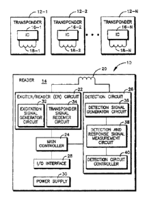
Figure 1 is a block diagram of an RFID system having a detection circuit of
the present invention.
Figure 2 is a schematic view of the detection signal generator circuit
included
within the RFID system and, more particularly, within the detection circuit of
Figure
1.
Figure 3a is a conceptualized view of an idealized coupled oscillator system,
which is conceptually representative of the detection signal generator circuit
of
Figure 2, in the symmetric mode of oscillation.
Figure 3b is a conceptualized view of the coupled oscillator system of Figure
3a in the anti-symmetric mode of oscillation.
Figure 4a is a conceptualized view of an alternate idealized coupled
oscillator
system in the symmetric mode of oscillation.
Figure 4b is a conceptualized view of the coupled oscillator system of Figure
4a in the anti-symmetric mode of oscillation.
Figure 5 is a conceptualized view of the coupled oscillator system of Figures
4a and 4b showing the system drivers.
Figure 6 is a schematic view of a stand-alone detection circuit of the present
invention.
Embodiments of the invention are illustrated by way of example and not by
way of limitation in the above-recited figures of the drawings in which like
reference
characters indicate the same or similar elements. It should be noted that
common
references to "an embodiment", "one embodiment", "an alternate embodiment", "a
preferred embodiment", or the like herein are not necessarily references to
the same
embodiment.
11
CA 02582554 2007-03-22
053P0503
DESCRIPTION OF PREFERRED EMBODIMENTS
An RFID system is shown in Figure 1 and generally designated 10. The RFID
system 10 comprises a plurality of transponders 12-1 through 12-N and a reader
14.
The transponders 12-1 through 12-N are preferably passive transponders which
do
not require an internal power supply. Instead the electrical power required to
operate the passive transponders is supplied to the transponders by
electromagnetic
energy transmitted from a reader. Accordingly, the passive transponders are
operational when they receive electromagnetic oscillations from a reader,
which are
of a specific frequency and of a sufficient strength to power up the
transponder.
Each transponder 12 comprises a number of functional elements including a
transponder integrated circuit (IC) 16 and a transponder antenna 18. The
transponder IC 16 embodies the processing and memory capabilities of the
transponder 12. The transponder antenna 18 is coupled to the transponder IC 16
and is a conventional coil termed a "dual-function antenna coil" which
performs both
the receiving and transmitting functions of the transponder 12. Alternatively,
two
separate receiving and transmitting antenna coils (not shown) can be
substituted for
the single "dual function antenna coil" in the transponder 12. The transponder
12
also preferably includes an external transponder tuning capacitor (not shown)
coupled to the transponder IC 16 and the transponder antenna 18. The term
"external" is used above with respect to the transponder 12 to designate
electronic
components which are not physically or functionally included within the
transponder
IC 16. The transponder antenna 18, in cooperation with the transponder tuning
capacitor, determines the tuned resonant frequency of the transponder LC pair
and
correspondingly the carrier frequency of the transponder 12.
The transponders 12 shown and described herein are but examples of types
of transponders having utility in the RFID system 10. It is understood that
practice of
the present invention is not limited to any specific types of transponders,
but is
generally applicable to most conventional types of transponders having utility
in
RFID systems. Thus, for example, the transponders 12 can be selected from
proximity cards, proximity tags, smart cards, or the like.
12
CA 02582554 2007-03-22
053P0503
In most conventional RFID systems, the position of the reader is stationary
(i.e., constant) relative to the surrounding environment, while the position
of the
transponder is portable (i.e., variable) within the surrounding environment.
In such
cases, the user of the RFID system moves the portable transponder into
relative
proximity with the stationary reader to enable simultaneous operation of the
both the
transponder and reader. In some conventional RFID systems, however, the
position
of the reader may be portable relative to the surrounding environment, while
the
position of the transponder is either portable or stationary. In the case of a
portable
reader and a stationary transponder, the user moves the portable reader into
relative
proximity with the stationary transponder to enable simultaneous operation of
both
the transponder and reader. In the case of a portable reader and a portable
transponder, the user may move both the portable reader and the portable
transponder into relative proximity with one another to enable simultaneous
operation of both the transponder and reader. Embodiments of the present
invention are not limited to any one of the above-recited RFID system
configurations.
The reader 14 comprises a number of functional elements including a reader
antenna assembly 20, an exciter/reader (ER) circuit 22, a main controller 24,
a
detection circuit 26, an input/output (I/O) interface 28, and a power supply
30. The
power supply 30 provides electrical operating power to the reader components
in a
controlled manner. In accordance with one embodiment, the power supply 30 is
coupled to a finite electrical power source which is self-contained (i.e.,
internal)
within the reader 14, such as a relatively small portable battery consisting
of one or
more disposable dry cells or rechargeable cells. Alternatively, the power
supply 30
is hard wired to an essentially infinite remote electrical power source, such
as an
electric utility.
The ER circuit 22 comprises an excitation signal generator circuit 32 and a
transponder signal receiver circuit 34. The excitation signal generator
circuit 32
generally functions to generate an excitation signal which the reader antenna
assembly 20 transmits in the form of electromagnetic oscillations into the
open
space of the external environment surrounding the reader 14. The excitation
signals
13
CA 02582554 2007-03-22
053P0503
are received by a transponder 12 in the proximal space of the reader 14 (i.e.,
within
a read range of the reader) to power up the transponder 12. Upon activation,
the
transponder IC 16 generates a transponder data signal, which contains readable
information (i.e., transponder data) copied or otherwise derived from the
memory of
the transponder IC 16. The transponder data signal is transmitted into the
open
space of the external environment surrounding the transponder 12 via the
transponder antenna 18. When a transponder data signal is received at the
reader
antenna assembly 20, the transponder signal receiver circuit 34 performs
various
operations on the transponder data signal to condition the signal, thereby
producing
a conditioned signal which is suitable for reading by the reader 14.
The conditioned signal containing the data from the transponder data signal is
conveyed to the main controller 24, which processes the conditioned signal to
extract the readable transponder data contained therein. In particular, the
main
controller 24 demodulates the conditioned signal in accordance with a
respective
modulation type according to firmware and/or software executed by the main
controller 24. The extracted transponder data may be sent to an external
device
such as a central host computer (not shown) via the I/O interface 28.
As noted above, the excitation signal generator circuit 32 and the transponder
signal receiver circuit 34 in combination are termed the ER circuit 22. The ER
circuit
22 is a conventional circuit well known to the skilled artisan. Exemplary ER
circuits
having utility in the reader 14 are disclosed in U.S. Patents 4,730,188 to
Milheiser
(the '188 Patent), 5,541,574 to Lowe et al. (the '574 Patent), and 5,347,263
to
Carroll et al. (the '263 Patent), all of which are incorporated herein by
reference.
Skilled artisans can further appreciate that the reader 14 can be adapted to
include a
conventional writer circuit (not shown) which is capable of writing
programming
instructions or other information to a transponder by either contact or
contactless
means. The ER circuit and writer circuit in combination are termed an
exciter/reader/writer (ERW) circuit. The term "ER circuit" as used herein is
deemed
to be inclusive of ERW circuits.
The reader 14 comprises two states of operation, namely, a low power
14
CA 02582554 2007-03-22
053P0503
detection state and a high power data transaction state (alternately referred
to as a
"read state"), which has been described above. The low power detection state
is the
initial operating state of the reader 14, wherein the detection circuit 26
functions as a
transponder detector to actively seek any transponders 12 residing in the
surrounding space proximal to the reader 14. Since the ER circuit 22 and main
controller 24 are characterized as having a high power demand when performing
reader functions, the reader 14 is configured to deactivate most or all of the
components and functions associated with the ER circuit 22 and the main
controller
24 in the detection state. Substantial power savings are achieved by using the
detection circuit 26 as the sole or primary operating unit for performing the
transponder detection function in the detection state because the detection
circuit 26
is characterized as having a low power demand. Once a transponder 12 is
detected, the reader 14 switches to the high power data transaction state, but
automatically switches back to the low power detection state when the high
power
data transaction state is completed.
The detection circuit 26 comprises a detection signal generator circuit 36 and
a detection and response signal measurement circuit 38 coupled thereto. A
detection circuit controller 40 is coupled to the detection signal generator
circuit 36
and detection and response signal measurement circuit 38 to direct operation
of the
circuits 36, 38. In general, the detection and response signal measurement
circuit
38 is configured to measure values of a preselected detection parameter for
the
detection and response signals to determine if any transponder 12 is present
within
the read range of the reader 14. Well known detection parameters include
signal
decay rate and signal voltage. If a transponder 12 is detected within the read
range
of the reader 14, the detection circuit controller 40 sends a transponder
recognized
signal to the main controller 24 indicating that a transponder 12 has been
detected.
The main controller 24 activates the ER circuit 22 in response to the
transponder
recognized signal, thereby switching the reader 14 from the low power
detection
state to the high power data transaction state.
Figure 2 shows a preferred embodiment of the detection signal generator
CA 02582554 2007-03-22
053P0503
circuit 36 in association with the detection and response signal measurement
circuit
38, detection circuit controller 40, ER circuit 22 and main controller 24. The
detection signal generator circuit 36 is a coupled oscillator system
comprising a first
LC pair 50 (alternately termed an oscillator) and a second LC pair 52. As
such, the
first LC pair 50 has a first tuning capacitor 54 and a first inductance coil
56
(alternately termed an inductor). The second LC pair 52 similarly has a second
tuning capacitor 58 and a second inductance coil 60. Both first and second LC
pairs
50, 52 are coupled to ground 62 and are coupled to one another across a
coupling
capacitor 64. The first LC pair 50 is provided with first CMOS drivers 66 and
the
second LC pair 52 is similarly provided with second CMOS drivers 68. The CMOS
drivers 66, 68 are preferably embodied in one or more integrated circuit
chips.
The detection signal generator circuit 36 is coupled to the detection circuit
controller 40 across a signal/pulse node 70, a mode logic gate 72 (preferably
an
XOR gate), and an enable logic gate 74 (preferably a NAND gate), which are
positioned in series. In particular, the detection circuit controller 40 is
coupled to a
SIGNAL/PULSE output line 76, a MODE output line 78, and an ENABLE output line
80. The SIGNAL and MODE output lines 76, 78 are the inputs to the XOR gate 72.
The XOR gate 72 has an XOR output line 82, which along with the ENABLE output
line 80, are the inputs to the NAND gate 74. The NAND gate 74 has a NAND
output
line 84 which provides an input pulse to the second CMOS drivers 68. The
SIGNAL/PULSE output line 76 correspondingly provides an input pulse to the
first
CMOS drivers 66. The function of these pulses is described in greater detail
below.
The detection signal generator circuit 36 enables the reader 14 to detect two
or more of the transponders 12-1 through 12-N, each of which is tuned to a
different
resonant frequency and each of which correspondingly transmits a transponder
data
signal having a different carrier frequency, when the respective transponder
is
positioned within the read range of the reader 14. More particularly, the
detection
signal generator circuit 36 enables multiple transponder detection
capabilities by
generating multiple detection signals at different frequencies, while in the
low power
detection state. Still more particularly, the detection signal generator
circuit 36
16
CA 02582554 2007-03-22
053P0503
enables sequential generation of multiple detection signals by configuring the
circuit
36 as a coupled oscillator system.
Coupled oscillator systems are characterized as having multiple "normal
modes" of oscillation, alternately termed eigenfunctions, eigenvectors, and
the like.
In the ideal limit of a lossless system, oscillations resulting from the
normal modes of
a coupled oscillator system are orthogonal to one another. Furthermore, each
normal mode of the coupled oscillator system defines a single frequency of
oscillation, which is often unique to the respective normal mode. All possible
oscillations of a coupled oscillator system are linear combinations of
oscillations
resulting from the normal modes of the system. The set of possible behaviors
of a
coupled oscillator system include linear combinations where only one normal
mode
of oscillation of the system is active. Activation of only a single normal
mode is
achieved by exciting the coupled oscillator system in accordance with proper
initial
conditions readily determined by the skilled artisan.
Oscillations resulting from the different normal modes of a coupled oscillator
system do not exchange energy over time due to their orthogonal character.
Therefore, a coupled oscillator system starting with all its energy in one
normal
mode typically stays in that same normal mode for the duration of system
operation
absent any external influence. Accordingly, each normal mode of a coupled
oscillator system can be separately initiated and discretely maintained by
appropriate selection of the initial conditions. Appropriate selection of the
initial
conditions also permits selection of the particular frequency for a given
normal mode
as desired by the practitioner.
The detection signal generator circuit 36 shown and described herein is a
particular type of coupled oscillator system termed a "double tuned" LC
resonant
circuit because the circuit 36 contains two LC pairs 50, 52. The detection
signal
generator circuit 36 has two distinct normal modes of oscillation, one normal
mode is
termed a symmetric mode of oscillation and the other normal mode is termed an
anti-symmetric mode of oscillation. In accordance with the present preferred
embodiment, the detection signal generator circuit 36 is a symmetrically
configured
17
CA 02582554 2007-03-22
053P0503
circuit, wherein the respective inductors L of the LC pairs 50, 52 have values
essentially equal to one another and the respective capacitors C of the LC
pairs 50,
52 similarly have values essentially equal to one another. It is understood,
however,
that the present invention is not limited to symmetrically configured coupled
oscillator
systems, but alternately encompasses asymmetrically configured coupled
oscillator
systems which nevertheless have normal modes of oscillation.
Referring to Figures 3a and 3b, the topology for an idealized coupled
oscillator system is shown, which is conceptually representative of the
detection
signal generator circuit 36 of Figure 2. When the same reference characters
are
used in Figures 3a and 3b as Figure 2, the like reference characters designate
the
same or similar elements. The idealized coupled oscillator system, which is
generally designated 86, is shown operating in each of its two normal modes of
oscillation, i.e., the symmetric mode of oscillation is shown in Figure 3a and
the anti-
symmetric mode of oscillation is shown in Figure 3b. The appropriate initial
conditions for each mode of oscillation of the system 86 are achieved by
simultaneously applying a combination of two pulses to two points on the
system 86,
wherein the combination of pulses is unique to the respective mode of
oscillation. In
particular, applying a symmetric combination of pulses achieves the symmetric
mode of oscillation, while applying an anti-symmetric combination of pulses
achieves
the anti-symmetric mode of oscillation.
The oscillations resulting from the symmetric (S) mode shown Figure 3a are
characterized by equation (1) below:
( 1 ) 2B fS = 1 / (LC)'rz
The oscillations resulting from the anti-symmetric (A) mode shown in Figure
3b are characterized by equation (2) below:
(2) 2B fA = 1 / (L(C+2C'))'rZ
18
CA 02582554 2007-03-22
053P0503
Referring again to Figure 2, in practice, operation of the reader 14 in the
low
power detection state, and specifically operation of the detection signal
generator
circuit 36, is initiated by setting an enable logic signal on the ENABLE
output line 80
to high and conveying input pulses to the first and second CMOS drivers 66, 68
under the direction of the detection circuit controller 40. The input pulse to
the first
CMOS drivers 66 is the pulse on the NAND output line 84 and input pulse to the
second CMOS drivers 68 is the pulse on the SIGNAL/PULSE output line 76. Each
of the CMOS drivers 66, 68 simultaneously applies a square pulse to its
associated
LC pair 50, 52 in response to each input pulse it receives. Simultaneous
application
of the pulse to each LC pair 50, 52 causes both LC pairs 50, 52 to
simultaneously
resonate at a frequency which is a function of the applied pulse. Simultaneous
resonance of the first and second LC pairs 50, 52 in response to a pulse on
each LC
pair generates a single ring signal (alternately termed a detection signal
herein)
because the first and second LC pairs 50, 52 are coupled across the coupling
capacitor 64. Periodic application of multiple pulses simultaneously to each
LC pair
50, 52 results in a sequence of detection signals, which are transmitted on
the
antenna assembly 20 into the surrounding space proximal to the reader 14.
The detection signal generator circuit 36 fixes the detection frequency of
each
detection signal by selectively setting the mode logic signal on the MODE
output line
80. In particular, a detection frequency fs, which is characteristic of the
symmetric
mode of oscillation, is achieved by setting the mode logic signal on the MODE
output
line 80 to low (i.e., the control level of the MODE output line 78 is logic
0). This
setting causes the first CMOS drivers 66 to apply a pulse having a given drive
sense
to the first LC pair 50, while causing the second CMOS drivers 68 to
simultaneously
apply a pulse having the same drive sense to the second LC pair 50 (e.g.,
drive
sense of both pulses is positive). A detection frequency fA, which is
characteristic of
the anti-symmetric mode of oscillation, is achieved by setting the mode logic
signal
on the MODE output line 80 to high (i.e., the control level of the MODE output
line 78
is logic 1). This setting causes the first CMOS drivers 66 to apply a pulse
having a
given drive sense to the first LC pair 50, while causing the second CMOS
drivers 68
19
CA 02582554 2007-03-22
053P0503
to simultaneously apply a pulse having an opposite drive sense to the second
LC
pair 50 (e.g., drive sense of one pulse is positive while the drive sense of
the other
pulse is negative).
Transmission of a detection signal into the proximal space of the reader 14
elicits a response signal on the reader antenna assembly 20, which has
essentially
the same detection frequency as the corresponding detection signal. All of the
detection signals and resulting response signals are conveyed to the detection
and
response signal measurement circuit 38, which is coupled to the reader antenna
assembly 20. The detection and response signal measurement circuit 38
evaluates
these signals to determine whether a transponder 12 having a given transponder
frequency is in the read range of the reader 14.
In accordance with the present embodiment of Figure 2, the first inductance
coil 56 of the first LC pair 50 functions as the reader antenna assembly 20
shown in
Figure 1. As such, the detection signals generated by the detection signal
generator
circuit 36 are transmitted on the first inductance coil 56 and the resulting
response
signals occur on the same coil 56. However, it is within the scope of the
present
invention for the second inductance coil 60 to alternatively function as the
reader
antenna assembly 20. In still other alternatives, both inductance coils 56, 60
can
function as the reader antenna assembly 20 or neither can function as the
reader
antenna assembly 20. In the case where neither coil 56, 60 functions as the
reader
antenna assembly 20, a separate antenna coil (not shown) coupled to the
detection
circuit 26 is provided to transmit the detection signals and elicit the
resulting
response signals.
When a transponder 12 is detected in the read range of the reader 14, it is
desirable to switch operation of the reader 14 to the high power data
transaction
state by configuring the detection signal generator circuit 36 so that the
reader 14
can function in a conventional manner. The reader 14 is transitioned to the
data
transaction state by setting the enable logic signal on the ENABLE output line
80 to
low. The signal on the SIGNAL/PULSE output line 76 is a digital signal
generated
by the ER circuit 22 in the form of a CW square wave carrier signal for
simplex
CA 02582554 2007-03-22
053P0503
transponders or a modulated carrier signal for duplex transponders. In this
configuration, the output signal from the first CMOS drivers 66 becomes a DC
ground sink signal for the carrier signal on the first inductance coil 56 and
the
second LC pair 52 behaves as a low pass filter.
Low power operation of the detection signal generator circuit 36 is described
above in a single mode of oscillation. However, the detection signal generator
circuit
36 can also be operated at low power in mixed mode of oscillation. The enable
logic
signal on the ENABLE output line 80 is set to low in the same manner as high
power
operation, but a square pulse rather than a carrier signal is transmitted on
the
SIGNAL/PULSE output line 76 to achieve a mixed mode of oscillation.
The detection signal generator circuit 36 is described herein as having two
coupled LC pairs 50, 52 only by way of example, and not by way of limitation.
It is
understood that the present invention embodies alternate detection signal
generator
circuits configured as coupled oscillator systems having three or more coupled
LC
pairs which enable detection of three or more of the transponders 12-1 through
12-
N, each of which is tuned to a different resonant frequency. The construction
and
operation of such alternate detection signal generator circuits is readily
within the
purview of the skilled artisan applying the teaching disclosed herein. Such
alternate
detection signal generator circuits are set into a normal mode of oscillation
using
appropriate initial conditions selected by properly choosing the phase and/or
amplitude of the pulses at various points in the circuit.
It is further understood that the present invention embodies detection signal
generator circuits having two coupled LC pairs in the manner of the circuit of
Figure
2, but having alternate topologies. For example, the topology for an alternate
embodiment idealized coupled oscillator system having two coupled LC pairs is
shown in Figures 4a and 4b and generally designated 88. When the same
reference
characters are used in Figures 4a and 4b as Figure 2, the like reference
characters
designate the same or similar elements. The idealized coupled oscillator
system 88
is shown operating in each of its two normal modes of oscillation, i.e., the
symmetric
mode of oscillation is shown in Figure 4a and the anti-symmetric mode of
oscillation
21
CA 02582554 2007-03-22
053P0503
is shown in Figure 4b. Figure 5 is a conceptualized representation of the
idealized
coupled oscillator system of Figures 4a and 4b which shows the drivers for the
system. The logic to create pulses in the system 88 of Figures 4a, 4b and 5 is
essentially the same as the logic of the detection signal generator circuit 36
of Figure
2.
The present invention is further a method for processing a sequence of
measurements of a predetermined detection parameter for the detection signals
and
response signals, wherein each detection and response signal either has the
frequency associated with the symmetric mode of oscillation or the frequency
associated with the anti-symmetric mode of oscillation. In accordance with the
signal processing method, the detection signal generator circuit 36 of the
reader 14
selectively generates a specific sequence of first and second detection
signals while
in the low power detection state, wherein the first detection signals have a
first
frequency associated with the symmetric mode and the second detection signals
have a second frequency associated with the anti-symmetric mode. The detection
signal generator circuit 36 applies the sequence of detection signals to the
reader
antenna assembly 20 which results in a corresponding sequence of response
signals on the reader antenna assembly 20.
An exemplary sequence of detection signals generated by the detection
signal generator circuit 36 is represented by a sequence of multiplexed
measurements. The sequence of measurements appears as follows:
...SASASASASASASASASASASASA...
"S" represents a measurement of the first detection signal having a shape
characteristic of the case where no transponder 12 is residing in the
surrounding
space proximal to the reader 14. As described above, the first detection
signal has
the first frequency associated with the symmetric mode and is produced by
simultaneously applying a symmetric combination of pulses to both LC pairs 50,
52
of the detection signal generator circuit 36. "A" similarly represents a
measurement
22
CA 02582554 2007-03-22
053P0503
of the second detection signal having a shape characteristic of the case where
no
transponder 12 is residing in the surrounding space proximal to the reader 14.
As
described above, the second detection signal has the second frequency
associated
with the anti-symmetric mode and is produced by simultaneously applying an
anti-
symmetric combination of pulses to both LC pairs 50, 52 of the detection
signal
generator circuit 36.
Because the detection circuit controller 40 selects the pulse combinations for
generating the detection signals, the reader firmware or hardware provides the
reader 14, and more preferably the detection circuit controller 40, with means
for
demultiplexing and separately processing measurements, which are derived from
the above-recited multiplexed sequence of measurements, as two subsequences of
measurements, respectively. The two subsequences of measurements appear as
follows:
...SSSSSSSSSSSS...
and
...AAAAAAAAAAAA...
The reader 14, and more preferably the detection circuit controller 40, is
further provided with means for distinguishing between measurements of the
detection signals and response signals. "s" represents a measurement of a
first
response signal which results from the case where a transponder 12, which is
tuned
at or near the first frequency fs associated with the symmetric mode of
oscillation, is
residing in the surrounding space proximal to the reader 14. "a" similarly
represents
a measurement of a second response signal which results from the case where a
transponder 12, which is tuned at or near the second frequency fA associated
with
the anti-symmetric mode of oscillation, is residing in the surrounding space
proximal
to the reader 14. Thus, the reader 14, and more preferably the detection
circuit
controller 40, is provided with means to distinguish between measurements of
"S"
and "s" and between measurements of "A" and "a". An exemplary distinguishing
23
CA 02582554 2007-03-22
053P0503
means is a technique wherein measured values are compared to predetermined
threshold levels. The reader 14 may still further be provided with means for
applying
digital or other filtering techniques to each subsequence of measurements so
that
the threshold level for each measurement subsequence can be slowly adjusted
over
time in response to drift caused by component aging or environmental factors
unrelated to the presence of a transponder 12 proximal to the reader 14.
When a transponder 12, which has a resonant frequency nearer fs than fA, is
positioned proximal to the reader 14, the resulting sequence of measurements
for
the detection and response signals on the reader antenna assembly 20 appears
as
follows:
... S A S A S A S A s A s A s A s A s A s A s A s A...
Similarly, when a transponder 12, which has a resonant frequency nearer fA
than fs, is positioned proximal to the reader 14, the resulting sequence of
measurements for the detection and response signals on the reader antenna
assembly appears as follows:
...SASASASASaSaSaSaSaSaSaSa...
In either case, the reader 14 is able to detect a transponder 12 positioned
within the proximal space of the reader 14 by detecting a change from "S" to
"s" or
from "A" to "a" within the appropriate subsequence of measurements. It is
noted that
if a transponder 12 is positioned close enough to the reader 14, the resulting
coupling may enable both modes of response signals, in which case the reader
14
may detect the transponder 12 by detecting a change within either subsequence
of
measurements.
Once the reader 14, which is functioning in the low power detection state
detects a transponder 12 in the above-described manner, the reader 14 switches
to
the high power detection state. The reader 14 automatically switches back to
the
24
CA 02582554 2007-03-22
053P0503
low power detection state when the high power data transaction state is
completed,
awaiting the detection of another transponder 12.
The above-recited exemplary sequence of measurements for detection and
response signals is termed an alternating sequence insofar as each measurement
alternates between S (or s) and A (or a). It is apparent to the skilled
artisan that any
number of other types of sequences may be utilized within the scope of the
present
invention. For example, non-alternating, balanced sequences can be generated
in
accordance with the present invention, which are derived from non-alternating,
balanced pulse rates (e.g., ...S S A A S S A A S S a a S S a a...). A non-
alternating,
balanced sequence is defined as a sequence of measurements, wherein the entire
sequence is approximately equally distributed between S (or s) and A (or a),
but
each measurement of the sequence does not alternate between S (or s) and A (or
a). Similarly non-alternating, unbalanced sequences can be generated in
accordance with the present invention, which are derived from non-alternating,
unbalancedpulserates(e.g.,...SASSSSASAAASaSSSSaSaaa...).
Referring to Figure 6, an alternate construction of the detection circuit is
shown and generally designated 100. The detection circuit 100 differs from the
detection circuit 26 in that the detection circuit 100 is constructed to
function as a
stand-alone transponder detector apart from the reader 14. When the same
reference characters are used in Figure 6 as Figure 2, the like reference
characters
designate the same or similar elements, which are common to both embodiments
of
the detection circuits 26 and 100 shown in Figures 2 and 6, respectively.
The detection circuit 100 comprises a detection signal generator circuit 102,
the detection and response signal measurement circuit 38, and the detection
circuit
controller 40. The detection and response signal measurement circuit 38 and
the
detection circuit controller 40 are essentially the same as those of the
detection
circuit 26 and the detection signal generator circuit 102 is essentially the
same as
the detection signal generator circuit 36 except for exclusion of the NAND
gate 74,
ENABLE output line 80, and NAND output line 84 from the detection signal
generator circuit 102. As such, the detection signal generator circuit 102 is
a
CA 02582554 2007-03-22
053P0503
coupled oscillator system comprising the first and second LC pairs 50, 52.
Both first
and second LC pairs 50, 52 are coupled to ground 62 and are coupled to one
another across the coupling capacitor 64. The first and second LC pairs 50, 52
are
provided with the first and second CMOS drivers 66, 68, respectively.
The detection signal generator circuit 102 is coupled to the detection circuit
controller 40 across the signal/pulse node 70 and XOR gate 72, which are
positioned in series. In particular, the detection circuit controller 40 is
coupled to the
SIGNAL/PULSE output line 76 and the MODE output line 78. The SIGNAL/PULSE
and MODE output lines 76, 78 are the inputs to the XOR gate 72. The XOR output
line 82 provides the input pulse to the second CMOS drivers 68. The
SIGNAL/PULSE output line 76 correspondingly provides the input pulse to the
first
CMOS drivers 66. The function of these signals is essentially the same as
described above with respect to the detection signal generator circuit 36.
Accordingly, the detection signal generator circuit 102 enables detection of
two or
more of the transponders 12-1 through 12-N, each of which is tuned to a
different
resonant frequency and each of which correspondingly transmits a transponder
data
signal having a different carrier frequency, when the respective transponders
are
positioned proximal to the circuit 102.
While the forgoing preferred embodiments of the invention have been
described and shown, it is understood that alternatives and modifications,
such as
those suggested and others, may be made thereto and fall within the scope of
the
invention. For example, although the detection signal generator circuit and
the
detection and response signal measurement circuit are shown and described
above
as being separate from the ER circuit, it is within the purview of the skilled
artisan to
partially or entirely incorporate the detection signal generator and detection
and
response signal measurement circuits into the ER circuit. There is also the
possibility of sharing certain specified components between the circuits. It
is further
within the purview of the skilled artisan to alternately integrate some or all
of the
functions and/or structure of the detection circuit controller into the main
controller or
vice versa. It is still further within the purview of the skilled artisan to
integrate some
26
CA 02582554 2007-03-22
053P0503
or all of the functions and/or structure of the detection and response signal
measurement circuit into the detection circuit controller. Such alternatives
and
modifications are within the scope and contemplation of the present invention.
27