Note: Descriptions are shown in the official language in which they were submitted.
CA 02583020 2011-04-05
POLY(ALKYNYLTHIOPHENE)S AND ELECTRONIC DEVICES
GENERATED THEREFROM
CROSS-REFERENCE TO RELATED APPLICATIONS
[0001] U.S. Patent Application Publication No. 2007-0260069, filed
concurrently herewith, on Functionalized Heteroacenes and Electronic
Devices Generated Therefrom, by Yuning Li et al.
[0002] U.S. Patent No. 7,550,760, filed concurrently herewith, on
Functionalized Heteroacenes, by Yuning Li et al.
[0003] U.S. Patent No. 7,557,370, filed concurrently herewith, on
Polyacenes and Electronic Devices Generated Therefrom, by Yuning Li et al.
[0004] U.S. Patent Application Publication No. 2007-0227042, filed
concurrently herewith, on Heteroacene Polymers and Electronic Devices
Generated Therefrom, by Yuning Li et al.
[0005] U.S. Patent No. 7,795,373, filed concurrently herewith, on
Ethynylene Acene Polymers and Electronic Devices Generated Therefrom, by
Yuning Li et al.
[0006] U.S. Patent No. 7,449,715, filed concurrently herewith, on
Ethynylene Acene Polymers, by Yuning Li et al.
[0007] U.S. Patent No. 7,563,860, filed concurrently herewith, on
Poly[bis(ethynyl)heteroacenes] and Electronic Devices Generated Therefrom,
by Yuning Li et al.
-1-
CA 02583020 2011-04-05
[0008] U.S. Patent No. 7,615,607, filed concurrently herewith, on
Semiconductors and Electronic Devices Generated Therefrom, by Yiliang Wu
et al.
[0009] U.S. Patent No. 7,517,477, filed concurrently herewith, on
Semiconductor Polymers, by Yiliang Wu et al.
[0010] U.S. Patent No. 7,619,055, filed concurrently herewith, on
Polydiazaacenes and Electronic Devices Generated Therefrom, by Yiliang Wu
et al.
[0011] U.S. Patent Application Publication No. 2007-0235719, filed
concurrently herewith, on Polydiazaacenes, by Yiliang Wu et al.
[0012] U.S. Patent No. 7,705,111, filed concurrently herewith, on
Poly(alkynylthiophene)s, by Beng S. Ong et al.
[0013] U.S. Patent No. 7,619,055, filed concurrently herewith, on
Linked Arylamine Polymers and Electronic Devices Generated Therefrom, by
Yuning Li et al.
[0014] U.S. Patent No. 7,847,052, filed concurrently herewith, on
Linked Arylamine Polymers, by Yuning Li et al.
[0015] Illustrated in U.S. Patent Application No. 2006-0124921, filed
December 14, 2004 relating to indolocarbazole moieties and thin film
transistor devices thereof.
[0016] Illustrated in U.S. Patent No. 7,402,681, filed June 27, 2005
relating to indolocarbazole moieties and thin film transistor devices thereof.
[0017] Illustrated in U.S. Patent 6,770,904 and U.S. Patent No.
7,250,625, Publication No. 20050017311, are electronic devices, such as thin
-2-
CA 02583020 2011-04-05
film transistors containing semiconductor layers of, for example,
polythiophenes.
[0018] In aspects of the present disclosure, there may be selected the
appropriate substituents, such as a suitable hydrocarbon, a heteroatom
containing group, hydrogen, halogen, CN, NO2, rings, number of repeating
polymer units, number of groups, and the like as illustrated in the copending
applications.
[0019] The appropriate components, processes thereof and uses
thereof illustrated in the copending applications and above patent may be
selected for the present invention in embodiments thereof.
STATEMENT REGARDING FEDERALLY SPONSORED RESEARCH OR
DEVELOPMENT
[0020] The electronic devices and certain components thereof were
supported by a United States Government Cooperative Agreement No.
70NANBOH3033 awarded by the National Institute of Standards and
Technology (NIST). The United States Government has certain rights relating
to the devices and certain semiconductor components illustrated hereinafter.
BACKGROUND
[0021] The present disclosure is generally directed to poly(3-
alkynylthiophene)s, substituted poly(3-alkynylthiophene)s, and uses thereof.
More specifically, the present disclosure in embodiments is directed to a
class
of poly(alkynyl substituted thiophene)s selected as solution processable and
substantially stable channel semiconductors in organic electronic devices,
such as thin film transistors.
-3-
CA 02583020 2007-03-30
[0022] There are desired electronic devices, such as thin film transistors
(TFTs), fabricated with poly(3-alkynylthiophene)s with excellent solvent
solubility,
which can be solution processable; and which devices possess mechanical
durability
and structural flexibility, characteristics which are desirable for
fabricating flexible
TFTs on plastic substrates. Flexible TFTs enable the design of electronic
devices
with structural flexibility and mechanical durability characteristics. The use
of plastic
substrates together with the poly(3-alkynylthiophene) component can transform
the
traditionally rigid silicon TFT into a mechanically more durable and
structurally flexible
TFT design. This can be of particular value to large area devices such as
large-area
image sensors, electronic paper and other display media. Also, the selection
of
poly(3-alkynylthiophene) TFTs for integrated circuit logic elements for low
end
microelectronics, such as smart cards, radio frequency identification (RFID)
tags, and
memory/storage devices, may enhance their mechanical durability, and thus
their
useful life span.
[0023] A number of semiconductor materials are not, it is believed, stable
when exposed to air as they become oxidatively doped by ambient oxygen,
resulting
in increased conductivity. The result is large off-current and thus low
current on/off
ratio for the devices fabricated from these materials. Accordingly, with many
of these
materials, rigorous precautions are usually undertaken during materials
processing
and device fabrication to exclude environmental oxygen to avoid or minimize
oxidative doping. These precautionary measures increase the cost of
manufacturing
therefore offsetting the appeal of certain semiconductor TFTs as an economical
alternative to amorphous silicon technology, particularly for large area
devices.
These and other disadvantages are avoided or minimized in embodiments of the
present disclosure.
-4-
CA 02583020 2007-03-30
REFERENCES
[0024] Regioregular polythiophenes, when selected as the semiconductor
layer for thin film transistors (TFTs), are sensitive to air and unstable when
exposed
to oxygen, that is for example, to photoinduced oxidative doping in air, a
disadvantage avoided or minimized with the thin film transistors disclosed
herein.
[0025] Acenes, such as pentacenes and heteroacenes, are known to possess
acceptable high filed effect mobility when used as channel semiconductors in
TFTs.
However, these materials are rapidly oxidized by, for example, atmospheric
oxygen
under light, and such compounds may not be considered processable at ambient
conditions. Furthermore, when selected for TFTs, acenes have poor thin film
formation characteristics and are substantially insoluble, thus they are
essentially
nonsolution processable; accordingly, such compounds have been mostly
processed
by vacuum deposition methods that result in high production costs, and which
disadvantages are minimized with the TFTs generated with the
poly(alkynylthiophene)s illustrated herein.
[0026] A number of organic semiconductor materials has been described for
use in field-effect TFTs, which materials include organic small molecules,
such as
pentacene, see for example D.J. Gundlach et al., "Pentacene organic thin film
transistors - molecular ordering and mobility", IEEE Electron Device Lett.,
Vol. 18, p.
87 (1997); oligomers, such as sexithiophenes or their variants, see for
example
reference F. Garnier et al., "Molecular engineering of organic semiconductors:
Design
of self-assembly properties in conjugated thiophene oligomers", J. Amer. Chem.
Soc., Vol. 115, p. 8716 (1993), and poly(3-alkylthiophene), see for example
reference
Z. Bao et al., "Soluble and processable regioregular poly(3-hexylthiophene)
for field-
effect thin film transistor application with high mobility", Appl. Phys. Lett.
Vol. 69,
p4108 (1996). Although organic material based TFTs generally provide lower
performance characteristics than their conventional silicon counterparts, such
as
-5-
CA 02583020 2007-03-30
silicon crystals or polysilicon TFTs, they may nonetheless be sufficiently
useful for
applications in areas where high mobility is not required.
[0027] Also, a number of known small molecule or oligomer-based TFT
devices rely on difficult vacuum deposition techniques for fabrication. Vacuum
deposition is selected primarily because these materials are either insoluble
or their
solution processing by spin coating, solution casting, or stamp printing does
not
generally provide uniform thin films.
[0028] Further, vacuum deposition may also involve the difficulties of
achieving
consistent thin film quality for large area format. Polymer TFTs, such as
those
fabricated from regioregular components of, for example, regioregular
poly(alkylthiophene-2,5-diyl) by solution processes, while offering some
mobility,
suffer from their propensity towards oxidative doping in air. The TFTs
fabricated from
these materials in ambient conditions generally, it is believed, exhibit large
off-
current, very low current on/off ratios, and their performance characteristics
degrade
rapidly. For low cost TFT design with excellent characteristics, it is
therefore of value
to have a semiconductor material that is both stable and solution processable,
and
where its performance is not adversely affected by ambient oxygen, for
example,
TFTs generated with the poly(3-al kynylthiophene)s illustrated herein.
[0029] Illustrated in Huang, D.H., et al, Chem. Mater. 2004, 16, 1298-1303,
are, for example, LEDS and field effect transistors based on certain
phenothiaazines
like poly(10-(2-ethyl hexyl)phenothiaazine).
[0030] Illustrated in Zhu, Y., et al, Macromolecules 2005, 38, 7983-7991, are,
for example semiconductors based on phenoxazine conjugated polymers like
poly(10-hexyl phenoxazi ne).
[0031] Additional references that may be of interest include U.S. Patent Nos.
6,150,191; 6,107,117; 5,969,376; 5,619,357, and 5,777,070.
-6-
CA 02583020 2011-04-05
SUMMARY OF THE INVENTION
[0031 a] In accordance with another aspect, there is provided an
electronic device comprising a semiconductive material of Formula (I):
R
n
(I)
wherein R is alkylaryl; and n represents the number of repeating units.
[0031 b] In accordance with a further aspect, there is provided a thin film
transistor device comprised of a substrate, a gate electrode, a gate
dielectric
layer, a source electrode and a drain electrode, and in contact with the
source/drain electrodes and the gate dielectric layer a semiconductor layer
comprising a homopolymer of Formula (I):
R
n
(I)
and wherein R is alkylaryl; and n represents the number of repeating units
[0031 c] In accordance with another aspect, there is provided a thin film
transistor comprising a semiconductive material wherein said semiconductive
material is selected from the group consisting of those of Formulas (2), (6)
or
(7)
-6a-
CA 02583020 2011-04-05
R'
4 S n
(2)
R'
4C S n
(6)
R'
S n
(7)
wherein R' is methyl, ethyl, propyl, butyl, pentyl, hexyl, heptyl, octyl,
nonyl,
decyl, undecyl, dodecyl, tridecyl, tetradecyl, pentadecyl, hexadecyl,
heptadecyl, octadecyl, nonadecyl, eicosanyl, hydroxymethy, hydroxyethyl,
hydroxypropyl, hydroxybutyl, hydroxypeptyl, hydroxyhexyl, hydroxyheptyl,
-6b-
CA 02583020 2011-04-05
hydroxyootyl, hydroxynonyl, hydroxydecyl, hydroxyundecyl, hydroxydodecyl,
methoxyethyl, methoxypropyl, methoxybutyl, methoxypentyl, methoxyoctyl,
trifluoromethy, perfluoroethyl, perfluoropropyl, perfluorobutyl,
perfluoropentyl,
perfluorohexyl, perfluoroheptyl, perfluorooctyl, perfluorononyl,
perfluorodecyl,
perfluoroundecyl, or perfluorododecyl; and wherein n is from about 2 to about
200.
[0031 d] In accordance with a further aspect, there is provided an
electronic device comprising a homopolymer of Formula (2a) or (2b):
C5H11
ZSnn
(2a)
2C8H17
(2b)
wherein n represents the number of repeating units.
[0031e] In accordance with another aspect, there is provided a thin film
transistor device comprised of a substrate, a gate electrode, a gate
dielectric
layer, a source electrode and a drain electrode, and in contact with the
-6c-
CA 02583020 2011-04-05
source/drain electrodes and the gate dielectric layer a semiconductor layer
comprising a homopolymer of Formula (2a) or (2b):
C5H11
S n
(2a)
C8H17
S n
(2b)
wherein n represents the number of repeating units.
-6d-
CA 02583020 2007-03-30
BRIEF DESCRIPTION OF THE DRAWINGS
[0032] Illustrated in Figures 1 to 4 are various representative embodiments of
the present disclosure, and wherein a poly(3-alkynylthiophene), such as poly(3-
decynylthiophene), is selected as the channel or semiconductor material in
thin film
transistor (TFT) configurations.
DESCRIPTION OF THE EXEMPLARY EMBODIMENTS
[0033] It is a feature of the present disclosure to provide a semiconductor,
poly(3-alkynylthiophene), which is useful for microelectronic device
applications, such
as TFT devices.
[0034] It is another feature of the present disclosure to provide a poly(3-
alkynylthiophene) with a band gap of from about 1 eV to about 3 eV as
determined
from the absorption spectra of thin films thereof, and which poly(3-
alkynylthiophene)
is suitable for use as TFT semiconductor channel layer materials.
[0035] In yet a further feature of the present disclosure there are provided
poly(3-alkynylthiophene)s, which are useful as microelectronic components, and
which poly(3-alkynylthiophene)s possess solubility of, for example, at least
about 0.1
percent to about 95 percent by weight in common organic solvents, such as
methylene chloride, tetrahydrofuran, toluene, xylene, mesitylene,
chlorobenzene, and
the like, and thus these components can be economically fabricated by solution
processes such as spin coating, screen printing, stamp printing, dip coating,
solution
casting, jet printing, and the like.
[0036] Also, in yet another feature of the present disclosure there are
provided
novel poly(alkynylthiophene)s, and devices thereof, and which devices exhibit
enhanced resistance to the adverse effects of oxygen, that is, these devices,
it is
believed, exhibit relatively high current on/off ratios, and their performance
may not
-7-
CA 02583020 2007-03-30
substantially degrade as rapidly as similar devices fabricated with
regioregular
poly(3-alkylthiophene-3,5-diyl) or with acenes.
[0037] Additionally, in a further feature of the present disclosure there is
provided a class of novel regioregular poly(3-alkynylthiophene)s, with unique
structural features which are conducive to molecular self-alignment under
appropriate
processing conditions, and which structural features also enhance the
stability of
device performance. Proper molecular alignment can permit higher molecular
structural order in thin films, which can be important to efficient charge
carrier
transport, thus higher electrical performance.
[0038] Further, another feature of the present disclosure relates to
regioregular
poly(3-alkynylthiophene)s by replacing the alkyl of polythiophene with an
alkynyl.
[0039] There are disclosed in embodiments, a poly(3-alkynylthiophene) and
electronic devices thereof. Alkynyl like ethynyl refers in embodiments to, for
example, a substituted ethynyl group in the poly(3-alkynylthiophene)s. Poly(3-
alkynylthiophene) refers in embodiments to, for example, a polymer which is
comprised of a repeat unit which is a thiophene with at least one pair of
optionally
substituted alkynyl like ethynyl groups.
[0040] More specifically, the present disclosure relates to
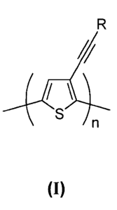
poly(alkynylthiophene)s illustrated by or encompassed by Formula (I)
R
n
(I)
wherein R is a suitable hydrocarbon, such as alkyl, aryl, and the like, and n
represents the number of repeating units, such as for example, n is a number
of from
about 2 to about 5,000, more specifically from about 10 to about 1,000, or
from about
20 to about 100.
-8-
CA 02583020 2007-03-30
[0041] In embodiments, the repeat unit can be considered the important
recurring unit of the polymer. The connection of the repeat units in the
polymer may
be identical, as is the situation with a regioregular polymer, or it may be
dissimilar, as
is the situation with a regiorandom polymer, and with respect primarily to the
directional aspect. Whether a repeat unit A is considered the same type or a
different
type as another repeat unit B is independent of directional aspect or sense
when
repeat unit A and repeat unit B are in the polymer. For instance, regiorandom
poly(3-
hexyithiophene) is considered to have only one type of repeat unit.
[0042] In embodiments, a specific class of regioregular poly(3-
alkynylthiophene)s is represented by the following formulas
R'
n
Znn
(2)
-9-
CA 02583020 2007-03-30
OR'
Zn
(3)
SR'
4Zn
(4)
O
4 I \
S
n
(5)
-10-
CA 02583020 2007-03-30
S
(6)
- R'
n
(7)
\ /R'
Si-'R,
WSn
(8)
wherein R' is a hydrocarbon of, for example, methyl, ethyl, propyl, butyl,
pentyl, hexyl,
heptyl, octyl, nonyl, decyl, undecyl, dodecyl, tridecyl, tetradecyl,
pentadecyl,
hexadecyl, heptadecyl, octadecyl, nonadecyl, eicosanyl, hydroxymethy,
hydroxyethyl,
hydroxypropyl, hydroxybutyl, hydroxypentyl, hydroxyhexyl, hydroxyheptyl,
hydroxyoctyl, hydroxynonyl, hydroxydecyl, hydroxyundecyl, hydroxydodecyl,
-11-
CA 02583020 2007-03-30
methoxyethyl, methoxypropyl, methoxybutyl, methoxypentyl, methoxyoctyl,
trifluoromethyl, perfluoroethyl, perfluoropropyl, perfluorobutyl,
perfluoropentyl,
perfluorohexyl, perfluoroheptyl, perfluorooctyl, perfluorononyl,
perfluorodecyl,
perfluoroundecyl, or perfluorododecyl; and wherein n is from about 2 to about
5,000,
from about 10 to about 200, or from about 20 to about 100.
[0043] In embodiments there are disclosed processes for the preparation of
poly(3-alkynylthiophene)s in accordance, for example, with the following
reaction
scheme (Scheme 1).
Scheme 1 - Synthesis of Poly(3-alkynyl thiophene)
R
I I /~
2 NBS ` _ R
S O Br S Br Br S Br
DMF, r.t. - 50 C Pd(PPh3)CI2,
Cul, Et3N, r.t.
R
R: -C8H17 (1 a)
C6H11MgCl
Ni(dppp)C12
THF, reflux S n C5H11 (2a)
More specifically, 2,5-dibromo-3-iodothiophene is prepared via bromination of
3-iodothiophene (available from Aldrich) with about 2 molar equivalents of
N-bromosuccinimide (NBS) in N,N-dimethylformamide (DMF) at room temperature,
about 23 C to about 26 C, and up to about 50 C. Thereafter, the 2,5-dibromo-3-
ethynylthiophene, such as 2,5-dibromo-3-decynylthiophene or 2,5-dibromo-3-(4-
pentyl phenyl)thiophene, is prepared by reacting 2,5-dibromo-3-iodothiophene
with
the corresponding ethynyl compound, decyne compound of less than 5 percent or
0
to 5 percent, or 1-ethynyl-4-butyl benzene in the presence of catalytic
amounts of
dichlorobis(triphenylphosphine)palladium (II) (Pd(PPh3)CI2 and copper (II)
iodide
-12-
CA 02583020 2007-03-30
(Cul) in triethylamine (Et3N) at room temperature. Subsequently, the poly(3-
ethynylthiophene), such as poly(3-decynylthiophene) (1a) or poly(3-(4-
pentylphenyl)ethynylthiophene) (2a), is generated by adding about one molar
equivalent of Grignard reagent, such as cyclohexylmagnesium chloride
(C6H11MgCI),
in the presence of [1,3-bis(diphenylphosphino)propane]dichioronickel (II)
(Ni(dppp)CI2) in refluxing tetrahydrofuran (THF).
[0044] Examples of R substituents include alkyl with, for example, from about
1 to about 30, including from about 4 to about 18 carbon atoms (included
throughout
are numbers within the range, for example 4, 5, 6, 7, 8, 9, 10, 11, 12, 13,
14, 15, 16,
17 and 18), such as eithyl, propyl, butyl, pentyl, hexyl, heptyl, octyl,
nonyl, decyl,
undecyl, dodecyl, tridecyl, tetradecyl, pentadecyl, hexadecyl, heptadecyl,
octadecyl,
nonadecyl, or eicosanyl, and the like; aryl with from about 6 to about 54
carbon
atoms, from about 6 to about 36 carbon atoms, from about 6 to about 24 carbon
atoms, such as thienyl, phenyl, methylphenyl (tolyl), ethylphenyl,
propylphenyl,
butylphenyl, pentylphenyl, hexylphenyl, heptylphenyl, octylphenyl,
nonylphenyl,
decylphenyl, undecylphenyl, dodecyiphenyl, tridecylphenyl, tetradecylphenyl,
pentadecylphenyl, hexadecylphenyl, heptadecylphenyl, octadecylphenyl, and the
like,
inclusive, it is believed, of other suitable hydrocarbons not specifically
described.
[0045] Specific heteroatom containing groups are known and include, for
example, polyethers, trialkylsilyls, heteroaryls, and the like; and more
specifically,
thienyl, furyl and pyridiaryl. The hetero component can be selected from a
number of
known atoms like sulfur, oxygen, nitrogen, silicon, selenium, and the like.
[0046] Specific illustrative poly(3-al kynylthiophene) examples are
C8H17
(1 a)
-13-
CA 02583020 2007-03-30
C5H11
S
(2a)
C8H17
S
(2b)
wherein n represents the number of repeating units in the polymer; and wherein
n is
from about 20 to about 100.
[0047] The poly(3-alkynylthiophene)s in embodiments are soluble or
substantially soluble in common coating solvents, for example, in embodiments
they
possess a solubility of at least about 0.1, and more specifically, from about
0.5
percent to about 95 percent by weight in such solvents as methylene chloride,
1,2-
dichloroethane, tetrahydrofuran, toluene, xylene, mesitylene, chlorobenzene,
dichlorobenzene, and the like. Moreover, the poly(3-alkynylthiophene)s or
substituted thiophenes of the present disclosure, when fabricated as
semiconductor
channel layers in TFT devices, can provide, it is believed, a stable
conductivity of, for
-14-
CA 02583020 2007-03-30
example, from about 10-9 S/cm to about 10-4 S/cm, and more specifically, from
about
10-8 S/cm to about 10-5 S/cm as determined by conventional four-probe
conductivity
measurements.
[0048] It is believed that the poly(3-alkynylthiophene)s illustrated herein
when
fabricated from solutions as thin films of, for example, from about 10
nanometers to
about 500 nanometers, or from about 100 to about 300 nanometers in thickness
can
be more stable in ambient conditions than similar devices fabricated from
acenes like
pentacene or certain poly(alkylthiophene)s. When unprotected, the
aforementioned
poly(3-alkynylthiophene) materials and devices can be, it is believed,
generally stable
for a number of weeks rather than days or hours as is the situation with
poly(3-
alkylthiophene-2,5-diyl) after exposure to ambient oxygen, thus the devices
fabricated from the poly(3-alkynylthiophene) in embodiments of the present
disclosure can provide higher current on/off ratios, and their performance
characteristics may not substantially change as rapidly as pentacene or poly(3-
alkylthiophene-2,5-diyl) when no rigorous procedural precautions have been
taken to
exclude ambient oxygen during material preparation, device fabrication, and
evaluation. The poly(3-alkynylthiophene)s stability of the present disclosure
in
embodiments against oxidative doping, particularly for low cost device
manufacturing,
does not usually have to be handled in an inert atmosphere, and the processes
thereof are, therefore, simpler and more cost effective, and the fabrication
thereof
can be applied to large scale production processes.
[0049] Aspects of the present disclosure relate to an electronic device
comprising a semiconductive material of Formula (I)
R
n
(I)
-15-
CA 02583020 2007-03-30
wherein R is a suitable hydrocarbon or a heteroatom containing group; and n
represents the number of repeating units; a thin film transistor device
comprised of a
substrate, a gate electrode, a gate dielectric layer, a source electrode and a
drain
electrode, and in contact with the source/drain electrodes and the gate
dielectric layer
a semiconductor layer of Formula (I)
R
n
(I)
and wherein R is a suitable hydrocarbon or a heteroatom containing group; and
n
represents the number of repeating units; an electronic device comprising a
semiconductive material wherein said device is a thin film transistor, and
said
semiconductive material is selected from the group consisting of those of
Formulas
(1) through (8)
R'
S n
(1)
-16-
CA 02583020 2007-03-30
R'
Zn
(2)
OR'
4 S
(3)
SR'
4 / ZSn
(4)
-17-
CA 02583020 2007-03-30
O
S
(5)
R'
S
n
(6)
R'
n
(7)
-18-
CA 02583020 2007-03-30
\ R'
Sim R,
S
n
(8)
wherein R' is a hydrocarbon of alkyl, aryl, and the like, and more
specifically, is
methyl, ethyl, propyl, butyl, pentyl, hexyl, heptyl, octyl, nonyl, decyl,
undecyl, dodecyl,
tridecyl, tetradecyl, pentadecyl, hexadecyl, heptadecyl, octadecyl, nonadecyl,
eicosanyl, hydroxymethy, hydroxyethyl, hydroxypropyl, hydroxybptyl,
hydroxypentyl,
hydroxyhexyl, hydroxyheptyl, hydroxyoctyl, hydroxynonyl, hydroxydecyl,
hydroxyundecyl, hydroxydodecyl, methoxyethyl, methoxypropyl, methoxybutyl,
methoxypentyl, methoxyoctyl, trifluoromethy, perfluoroethyl, perfluoropropyl,
perfluorobutyl, perfluoropentyl, perfluorohexyl, perfluoroheptyl,
perfluorooctyl,
perfluorononyl, perfluorodecyl, perfluoroundecyl, or perfluorododecyl; and
wherein n
is from about 2 to about 200; a polymer of the following formula
R
n
(I)
wherein R is a suitable hydrocarbon or a heteroatom containing group; and n
represents the number of repeating units; a TFT device wherein the substrate
is a
plastic sheet of a polyester, a polycarbonate, or a polyimide; the gate source
and
drain electrodes are each independently comprised of gold, nickel, aluminum,
platinum, indium titanium oxide, or a conductive polymer, and the gate
dielectric is a
dielectric layer comprised of silicon nitride or silicon oxide; a TFT device
wherein the
-19-
GA 02583020 2007-03-30
substrate is glass or a plastic sheet; said gate, source and drain electrodes
are each
comprised of gold, and the gate dielectric layer is comprised of the organic
polymer
poly(methacrylate), or poly(vinyl phenol); a device wherein the poly(3-
alkynyithiophene) layer is formed by solution processes of spin coating, stamp
printing, screen printing, or jet printing; a device wherein the gate, source
and drain
electrodes, the gate dielectric, and semiconductor layers are formed by
solution
processes of spin coating, solution casting, stamp printing, screen printing,
or jet
printing; and a TFT device wherein the substrate is a plastic sheet of a
polyester, a
polycarbonate, or a polyimide, and the gate, source and drain electrodes are
fabricated from the organic conductive polymer polystyrene sulfonate-doped
poly(3,4-
ethylene dioxythiophene), or from a conductive ink/paste compound of a
colloidal
dispersion of silver in a polymer binder, and the gate dielectric layer is
organic
polymer or inorganic oxide particle-polymer composite; and device or devices
include
electronic devices such as TFTs.
DETAILED DESCRIPTION OF THE FIGURES
[0050] In Figure 1 there is schematically illustrated a TFT configuration 10
comprised of a substrate 16, in contact therewith a metal contact 18 (gate
electrode),
and a layer of an insulating dielectric layer 14 with the gate electrode
having a portion
thereof or the entire gate in contact with the dielectric layer 14 with the
gate electrode
having a portion thereof or the entire gate in contact with the dielectric
layer 14 on top
of which layer 14 two metal contacts, 20 and 22 (source and drain electrodes),
are
deposited. Over and between the metal contacts 20 and 22 is the semiconductive
polymer, such as poly(3-decynylthiophene), layer 12. The gate electrode can be
included in the substrate, in the dielectric layer, and the like throughout.
[0051] Figure 2 schematically illustrates another TFT configuration 30
comprised of a substrate 36, a gate electrode 38, a source electrode 40, and a
drain
-20-
CA 02583020 2007-03-30
electrode 42, an insulating dielectric layer 34, and a poly(3-
decynylthiophene)
semiconductor layer 32.
[0052] Figure 3 schematically illustrates a further TFT configuration 50
comprised of a heavily n-doped silicon wafer 56, which can act as a gate
electrode, a
thermally grown silicon oxide dielectric layer 54, a poly(3-decynylthiophene)
semiconductor layer 52, and a source electrode 60 and a drain electrode 62;
and a
gate electrode contact 64.
[0053] Figure 4 schematically illustrates a TFT configuration 70 comprised of
a
substrate 76, a gate electrode 78, a source electrode 80, a drain electrode
82, a
poly(3-decynylthiophene) semiconductor layer 72, and an insulating dielectric
layer
74.
[0054] Also, other devices not disclosed, especially TFT devices, are
envisioned, reference for example known TFT devices.
[0055] In some embodiments of the present disclosure, an optional protecting
layer may be incorporated on top of each of the transistor configurations of
Figures 1,
2, 3 and 4. For the TFT configuration of Figure 4, the insulating dielectric
layer 74
may also function as a protecting layer.
[0056] In embodiments, and with further reference to the present disclosure
and the Figures, the substrate layer may generally be a silicon material
inclusive of
various appropriate forms of silicon, a glass plate, a plastic film or a
sheet, and the
like depending on the intended applications. For structurally flexible
devices, a
plastic substrate, such as for example polyester, polycarbonate, polyimide
sheets,
and the like, may be selected. The thickness of the substrate may be, for
example,
from about 10 micrometers to over 10 millimeters with a specific thickness
being from
about 50 to about 100 micrometers, especially for a flexible plastic
substrate, and
from about 1 to about 10 millimeters for a rigid substrate such as glass or
silicon.
[0057] The insulating dielectric layer, which can separate the gate electrode
from the source and drain electrodes, and in contact with the semiconductor
layer,
can generally be an inorganic material film, an organic polymer film, or an
organic-
-21-
CA 02583020 2007-03-30
inorganic composite film. The thickness of the dielectric layer is, for
example, from
about 10 nanometers to about 1 micrometer with a more specific thickness being
about 100 nanometers to about 500 nanometers. Illustrative examples of
inorganic
materials suitable as the dielectric layer include silicon oxide, silicon
nitride,
aluminum oxide, barium titanate, barium zirconate titanate, and the like;
illustrative
examples of organic polymers for the dielectric layer include polyesters,
polycarbonates, poly(vinyl phenol), polyimides, polystyrene,
poly(methacrylate)s,
poly(acrylate)s, epoxy resin, and the like; and illustrative examples of
inorganic-
organic composite materials include nanosized metal oxide particles dispersed
in
polymers, such as polyester, polyimide, epoxy resin and the like. The
insulating
dielectric layer is generally of a thickness of from about 50 nanometers to
about 500
nanometers depending on the dielectric constant of the dielectric material
used.
More specifically, the dielectric material has a dielectric constant of, for
example, at
least about 3, thus a suitable dielectric thickness of about 300 nanometers
can
provide a desirable capacitance, for example, of about 10-9 to about 10-7
F/cm2.
[0058] Situated, for example, between and in contact with the dielectric layer
and the source/drain electrodes is the active semiconductor layer comprised of
the
poly(3-alkynylthiophene)s illustrated herein, and wherein the thickness of
this layer is
generally, for example, about 10 nanometers to about 1 micrometer, or about 40
to
about 100 nanometers. This layer can generally be fabricated by the solution
processing of the poly(3-alkynylthiophene)s of the present disclosure.
[0059] The gate electrode can be a thin metal film, a conducting polymer film,
a conducting film generated from a conducting ink or paste, or the substrate
itself (for
example heavily doped silicon). Examples of gate electrode materials include,
but
are not limited to aluminum, gold, chromium, indium tin oxide, conducting
polymers,
such as polystyrene sulfonate-doped poly(3,4-ethylenedioxythiophene)
(PSS/PEDOT), a conducting ink/paste comprised of carbon black/graphite or
colloidal
silver dispersion contained in a polymer binder, such as Electrodag available
from
Acheson Colloids Company, and silver filled electrically conductive
thermoplastic ink
-22-
CA 02583020 2007-03-30
available from Noelle Industries, and the like. The gate layer can be prepared
by
vacuum evaporation, sputtering of metals or conductive metal oxides, coating
from
conducting polymer solutions or conducting inks or dispersions by spin
coating,
casting or printing. The thickness of the gate electrode layer is, for
example, from
about 10 nanometers to about 10 micrometers, and a specific thickness is, for
example, from about 10 to about 200 nanometers for metal films, and about 1 to
about 10 micrometers for polymer conductors.
[0060] The source and drain electrode layer can be fabricated from materials
which provide a low resistance ohmic contact to the semiconductor layer.
Typical
materials suitable for use as source and drain electrodes include those of the
gate
electrode materials such as gold, nickel, aluminum, platinum, conducting
polymers,
and conducting inks. Typical thickness of this layer is about, for example,
from about
40 nanometers to about 1 micrometer with the more specific thickness being
about
100 to about 400 nanometers. The TFT devices contain a semiconductor channel
with a width W and length L. The semiconductor channel width may be, for
example,
from about 10 micrometers to about 5 millimeters with a specific channel width
being
about 100 micrometers to about 1 millimeter. The semiconductor channel length
may
be, for example, from about 1 micrometer to about 1 millimeter with a more
specific
channel length being from about 5 micrometers to about 100 micrometers.
[0061] The source electrode is grounded and a bias voltage of generally, for
example, about 0 volt to about -80 volts is applied to the drain electrode to
collect the
charge carriers transported across the semiconductor channel when a voltage of
generally about +10 volts to about -80 volts is applied to the gate electrode.
[0062] Other known materials not recited herein for the various components of
the TFT devices of the present disclosure can also be selected in embodiments.
[0063] Although not desiring to be limited by theory, it is believed that the
alkynyl like the ethynyl groups functions primarily to minimize or avoid
instability upon
exposure to oxygen thereby increasing the oxidative stability of the poly(3-
alkynylthiophene)s in solution under ambient conditions and the R
substituents, such
-23-
CA 02583020 2007-03-30
as alkyl, permit the solubility of these polymers in common solvents, such as
ethylene
chloride, tetrahydrofuran, toluene, chlorobenzene, d ichloro benzene, and the
like.
[0064] The following Examples are provided, it being understood that these
Examples are intended to be illustrative only, and the disclosure is not
intended to be
limited to the materials, conditions, or process parameters recited. All
percentages
and parts are by weight unless otherwise indicated. Identification of the
products
generated can be accomplished by a number of known methods including HNMR in
CdCl3.
EXAMPLE I
Synthesis of Poly(3-decynylthiophene) (1a):
[0065] 1) 2,5-Dibromo-3-iodothiophene
[0066] 3-lodothiophene (4.20 grams, 20 mmol) was dissolved in DMF (50
milliliters) under argon at room temperature. N-Bromosuccinimide (NBS) (7.83
grams, 40 mmol) in DMF (50 milliliters) was added to the above solution with
stirring.
The resulting mixture was then stirred at room temperature for 1 hour, and the
reaction temperature was raised to 50 C and held at this temperature for
another 3 to
4 hours. After removing the DMF solvent, the liquid resulting was dissolved in
ethylacetate and washed with water three times. The organic phase formed was
dried over anhydrous magnesium sulfate (MgSO4), and the solvent was removed.
Further purification was conducted by using column chromatography on a silica
gel
with hexane as an eluent. 2,5-Dibromo-3-iodothiophene was thus obtained as a
colorless liquid. Yield: 7 grams (95 percent).
[0067] 2) 2,5-Dibromo-3-decynylthiophene
[0068] To a solution of the above prepared 2,5-dibromo-3-iodothiophene (3.43
grams, 9.3 mmol) and 1-decyne (1.45 grams, 10.5 mmol) in triethylamine (50
milliliters) were added dichlorobis(triphenylphosphine)palladium (II) (0.28
gram, 0.4
mmol) and copper(I) iodide (38 milligrams, 0.2 mmol) at 0 C under argon. The
-24-
CA 02583020 2007-03-30
reaction mixture was stirred at 0 C for 6 hours and at room temperature for 20
hours
under argon. After evaporation of the solvent, the product was purified by
column
chromatography on silica gel using hexane as eluent. 2,5-Dibromo-3-
decynylthiophene was thus obtained as a colorless liquid was. Yield: 3.32
grams (94
percent).
[0069] 1H NMR (in CDCI3): 6.88 (s, 1 H), 2.41 (t, J = 7.0 Hz, 2H), 1.60 (m,
2H),
1.45 (m, 2H), 1.29 (br, 10 H), 0.88 (t, J = 6.4 Hz, 3H).
[0070] 3) Poly(3-decynylthiophene) (1 a)
[0071] A dry 100 milliliter three-neck flask was charged with the above
prepared 2,5-dibromo-3-decynylthiophene (1.89 grams, 5 mmol) and anhydrous THE
(50 milliliters). Then, 2M cyclohexylmagnesium chloride in diethyl ether (2.5
milliliters, 5 mmol) was added to the flask via syringe. The reaction mixture
was
allowed to stir for 30 minutes at room temperature followed by the addition of
Ni(dppp)C12 (41 milligrams, 0.075 mmol). The reaction mixture was then allowed
to
reflux for 12 hours. The reaction mixture was then allowed to cool down to
room
temperature, precipitated into methanol (200 milliliters), and filtered. The
polymer
resulting was purified by Soxhlet extraction in sequence with methanol (48
hours),
acetone (24 hours), and hexane (24 hours). Finally, the residue solid was
dissolved
with chloroform. After removing the solvent, the dark purple solid was dried
under
vacuum to yield poly(3-decynylthiophene) (1a). Yield: 0.50 gram (46 percent).
[0072] 1H NMR (in CDCI3): 7.09 - 7.33 (br), 2.56, 1.73, 1.51, 1.29, 0.87.
[0073] GPC (with polystyrene as standard): Mõ = 10,300; M IMn = 2.18.
Device Fabrication And Evaluation:
[0074] There was selected a top-contact thin film transistor configuration as
schematically illustrated, for example, in Figure 3. The device was comprised
of an
n-doped silicon wafer with a thermally grown silicon oxide layer of a
thickness of
about 110 nanometers thereon. The wafer functioned as the gate electrode while
the
-25-
CA 02583020 2007-03-30
silicon oxide layer acted as the gate dielectric and had a capacitance of
about 30
nF/cm2 (nanofarads/square centimeter) as measured with a capacitor meter. The
silicon wafer was first cleaned with isopropanol, argon plasma, and air dried.
Then,
the clean substrate was immersed in a 0.1 M solution of octyltrichlorosilane
(OTS8) in
toluene at 60 C for 20 minutes. Subsequently, the wafer was washed with
toluene,
isopropanol and air dried. Poly(3-decynylthiophene) (1a) dissolved in
dichlorobenzene at a concentration of 0.3 percent by weight was used to
deposit the
semiconductor layer. The solution was first filtrated through a 1 micrometer
syringe
filter, and then spin-coated on to the OTS8 silicon substrate at 1,000 rpm for
120
seconds at room temperature resulting in a thin film with thickness of about
20 to
about 50 nanometers. After being dried in a vacuum oven at 80 C for 5 to 10
hours,
gold source and drain electrodes of about 50 nanometers were deposited on top
of
the semiconductor layer by vacuum deposition through a shadow mask with
various
channel lengths and widths, thus creating a series of transistors of various
dimensions.
[0075] The evaluation of the generated field-effect transistor performance was
accomplished in a black box at ambient conditions using a Keithley 4200 SCS
semiconductor characterization system. The carrier mobility, , was calculated
from
the data in the saturated regime (gate voltage, VG < source-drain voltage,
VSD)
according to Equation (1)
Isp = C, (W/2L) (VG-VT)2 (1)
where Isp is the drain current at the saturated regime, W and L are,
respectively, the
semiconductor channel width and length, Ci is the capacitance per unit area of
the gate
dielectric layer, and VG and VT are, respectively, the gate voltage and
threshold
voltage. VT of the device was determined from the relationship between the
square
root of Isp at the saturated regime and VG of the device by extrapolating the
measured
data to Isp = 0.
-26-
CA 02583020 2007-03-30
[0076] Another property of a field-effect transistor is its current on/off
ratio.
This is the ratio of the saturation source-drain current at the accumulation
regime to
the source-drain current at the depletion regime.
[0077] The transfer and output characteristics of the devices revealed that
poly(3-decynylthiophene) (1a) is a p-type semiconductor. Evaluating about 5
transistors with a dimension of W = 5,000 m and L = 90 m resulted in
mobilities of
from about 1 to about 3, and more specifically, from 0.001 to about 0.008
cm2/Vs
(volts per second)
Mobility: 0.008 cm2V-1s 1
On/off ratio: 106.
EXAMPLE II
Synthesis of Poly(3-(4-pentylphenyl)ethynylthiophene) (2a):
[0078] 1) 2,5-Dibromo-3-(4-pentylphenyl)ethynylthiophene
[0079] To a solution of 2,5-dibromo-3-iodothiophene (3.52 grams, 9.57 mmol)
and 1-ethynyl-4-pentylbenzene (1.65 grams, 9.57 mmol) in triethylamine (50
milliliters) were added dichlorobis(triphenylphosphine)palladium (II) (0.28
gram, 0.4
mmol) and copper(l) iodide (38 milligrams, 0.2 mmol) at 0 C under argon. The
resulting reaction mixture was stirred at 0 C for 6 hours and at room
temperature for
20 hours under argon. After evaporation of the solvent, the product obtained
was
purified by column chromatography on a silica gel using hexane as eluent.
2,5-Dibromo-3-(4-pentylphenyl)ethynylthiophene was obtained as a colorless
liquid
was. Yield: 3 grams (73 percent).
[0080] 1H NMR (in CDCI3): 7.44 (d, J = 8.3 Hz, 2H), 7.16 (d, J = 8.3 Hz, 2H),
7.00 (s, 1 H), 2.61 (t, J = 7.7 Hz, 2H), 1.61 (m, 2H), 1.32 (m, 4H), 0.89 (t,
J = 6.8 Hz,
3H).
-27-
CA 02583020 2007-03-30
[0081] 2) Poly(3-(4-pentylphenyl)ethynylthiophene) (2a)
[0082] A dry 100 milliliter three-neck flask was charged with the above
prepared 2,5-dibromo-3-(4-pentylphenyl)ethynylthiophene (2.06 grams, 5 mmol)
and
anhydrous THE (50 milliliters). Then, 2M cyclohexylmagnesium chloride in
diethyl
ether (2.5 milliliters, 5 mmol) was added to the flask via a syringe. The
reaction
mixture resulting was allowed to stir for 30 minutes at room temperature
followed by
the addition of Ni(dppp)C12 (41 milligrams, 0.075 mmol). The reaction mixture
was
then allowed to reflux for 12 hours. The reaction mixture was then allowed to
cool
down to room temperature, precipitated into methanol (200 milliliters), and
filtered.
The polymer generated was purified by Soxhlet extraction in sequence with
methanol
(48 hours), acetone (24 hours), and hexane (24 hours). Finally, the residue
solid was
dissolved with chloroform. After removing solvent, the dark purple solid was
dried
under vacuum to yield poly(3-(4-pentylphenyl)ethynylthiophene) (2a). Yield:
0.20
gram (16 percent).
[0083] 'H NMR (in CDCI3): 7.41, 7.02, 2.51, 1.56, 1.32, 0.90.
[0084] GPC (with polystyrene as standard): Mn = 3,600; MW/Mõ = 1.41.
Device Fabrication And Evaluation:
[0085] OTFT devices using poly(3-(4-pentylphenyl)ethynylthiophene) (2a) as a
semiconductor layer were fabricated and evaluated similarly by repeating the
device
fabrication of Example I. The transfer and output characteristics of the
device
revealed that poly(3-(4-pentylphenyl)ethynylthiophene) (2a) is a p-type
semiconductor. Evaluating five (5) transistors with a dimension of W = 5,000
m and
L = 90 m there were obtained similar desirable characteristics of the devices
of
Example I.
Mobility: 0.001 cm2V-'s"'
On/off ratio: 106.
-28-
CA 02583020 2007-03-30
[0086] The claims, as originally presented and as they may be amended,
encompass variations, alternatives, modifications, improvements, equivalents,
and
substantial equivalents of the embodiments and teachings disclosed herein,
including
those that are presently unforeseen or unappreciated, and that, for example,
may
arise from applicants/patentees and others. Unless specifically recited in a
claim,
steps or components of claims should not be implied or imported from the
specification or any other claims as to any particular order, number,
position, size,
shape, angle, color, or material.
-29-