Note: Descriptions are shown in the official language in which they were submitted.
CA 02583661 2007-04-12
WO 2006/044563 PCT/US2005/036868
"INTEGRATEIY 1 fIPtS' Q,fRE"s'U ITRY FOR ULTRASOUND IMAGING DEVICES
FIELD OF THE INVENTION
The systems and methods relate generally to the use of bias circuitry for
biasing an
ultrasound imaging device in an intravascular ultrasound imaging system.
BACKGROUND INFORMATION
To generate an image using a medical ultrasound imaging system, such as an
intravascular ultrasound (IVUS) or intracardiac echocardiography (ICE) imaging
system, an
ultrasound imaging device, typically including one or more transducers, is
located on or within
an intravascular device, such as a catheter and the like. The intravascular
device is navigated
into the body and the imaging device is used to image the desired body tissue.
To do this, the
transducer generates and transmits an ultrasound pulse into the body tissue.
As this pulse
strikes various layers of body tissue, echoes are reflected back to and
received by the
transducer. The transducer generates an electrical output signal
representative of the strength
of the received echo and outputs this signal to an image processing system.
The image
processing system processes the signal and uses it to form an image of the
body tissue.
Conventionally, ultrasound transducers have been made of piezoelectric
materials
which require ceramic manufacturing technologies which are vastly different
from those used
to manufacture other components in an ultrasound imaging system, which are
typically
semiconductor-based. Piezoelectric transducers typically have a narrow
bandwidth which
limits the depth of tissue that can be imaged.
Recently, a new type of transducer has been developed capable of fabrication
with
semiconductor-based processing technologies. Capacitive micromachined
ultrasonic
transducers (CMUTs) were designed to answer a need to mass fabricate medical
ultrasound
transducers using the very same semiconductor manufacturing processes used to
fabricate the
other parts of an extern-al ultrasound imaging system. CMUTs are typically
much smaller than
piezoelectric transducers (on the order of 10 to 100 microns in size) and have
a larger
bandwidth.
A typical CIVIUT includes a drumhead structure suspended over a substrate in a
manner
to allow two-way conversion between a mechanical wave and an electrical signal
through
modulation of a capacitive charge on the drumhead. To deliver an ultrasound
pulse, the
capacitive charge on the drumhead, measured relative to a substrate electrode,
is modulated by
delivery of an electrical pulse to the drumhead. The delivery of this pulse
causes the drumhead
to vibrate and thereby transmit an ultrasound wave. Likewise, in the receiving
mode, the
-1-
CA 02583661 2007-04-12
WO 2006/044563 PCT/US2005/036868
iMPbLct'bt'We''echb1'ori'the,drurrnneuuimoaulates the capacitance and results
in an electrical
signal representative of the strength of the received echo.
CMUT devices are not currently used in IVLTS imaging systems. One reason for
this is
because in order to operate, the CMUT needs a constant bias voltage that is
carefully controlled
so as to maintain high transducer sensitivity without short-circuiting the
transducer's
capacitance. Accordingly, there is a need for systems and methods for applying
this bias
voltage to CMUT devices in intravascular ultrasound imaging systems.
SUMMARY
The systems and methods described herein provide for an imaging system having
bias
circuitry for applying a bias voltage to one or more transducers. In one
example embodiment,
the imaging system includes an imaging device insertable into a living being
and configured to
image the interior of the living being. The imaging device includes an
ultrasound transducer
and bias circuitry electrically coupled with the transducer and configured to
electrically bias the
transducer. The imaging device can be coupled with a rotatable driveshaft and
communicatively coupled with an image processing system. The image processing
system can
be configured to output a transducer drive signal to the transducer over a
signal line located
along the driveshaft and supply charge to the bias circuitry over the same
signal line.
Preferably, the transducer is CMUT capable of fabrication in a semiconductor-
based
manufacturing process. In one embodiment, the transducer is a CMUT and is
integrated with
the bias circuitry on a common semiconductor substrate. The bias circuitry can
include a
charge pump for accumulating the bias voltage and also charge limiting
circuitry for controlling
the bias voltage.
The systems and methods described herein also provide for an image processing
system
configured to operate an imaging device having bias circuitry. In one example
embodiment,
the image processing system can be configured to output a transducer drive
signal during a first
time period, receive a transducer output signal during a second time period
and output a bias
signal during a third time period. The transducer drive signal can be
configured to cause a
transducer within the imaging device to generate an ultrasound pulse. The
transducer output
signal is preferably representative of an echo received by the transducer. The
bias signal can be
configured to provide electrical charge to bias circuitry coupled with the
transducer.
The systems and methods described herein also provide for a method of
ultrasound
imaging with an image processing system. In one example embodiment, the method
includes
outputting a transducer drive signal during a first time period, where the
transducer drive signal
-2-
CA 02583661 2007-04-12
WO 2006/044563 PCT/US2005/036868
i'S c'bnt~~gdrdd'1to11datisb a trW9auDer,T0::transmit an ultrasound pulse. The
method also includes
receiving a transducer output signal during a second time period following the
first time period,
where the transducer output signal is representative of an echo received by
the transducer, and
outputting a bias signal during a third time period following the second time
period, where the
bias signal is configured to provide charge to bias circuitry. In another
example embodiment,
the method can include outputting a second bias signal during a fourth time
period prior to the
first time period, where the second bias signal output during the fourth time
period is
configured to initialize the bias circuitry. The fourth time period can also
be longer than the
third time period.
Other systems, methods, features and advantages of the invention will be or
will
become apparent to one with skill in the art upon examination of the following
figures and
detailed description. It is intended that all such additional systems,
methods, features and
advantages be included within this description, be within the scope of the
invention, and be
protected by the accompanying claims. It is also intended that the invention
is not limited to
require the details of the example embodiments.
BRIEF DESCRIPTION OF THE FIGURES
The details of the invention, including fabrication, structure and operation,
may be
gleaned in part by study of the accompanying figures, in which like reference
numerals refer to
like segments.
FIG. 1 is a schematic view depicting an example embodiment of an IVUS imaging
system.
FIG. 2 is a perspective view depicting another example embodiment of an IVUS
imaging system.
FIGs. 3A-B are cross-sectional views depicting an example embodiment of a
CMUT.
FIG. 4 is a block diagram depicting an example embodiment of an IVUS imaging
device.
FIG. 5 is a timing diagram depicting example output signals from an image
processing
system.
FIG. 6 is a flow diagram depicting a method of operating an imaging device
with an
image processing system.
DETAILED DESCRIPTION
The systems and methods described herein allow the application of a bias
voltage to one
or more transducers implemented within an imaging system. FIG. 1 depicts one
example
-3-
CA 02583661 2007-04-12
WO 2006/044563 PCT/US2005/036868
8ml4odlrnerit-16fgystd:i-Iut111aving bias circuitry 102. Preferably, the
imaging
system 100 is an IVUS imaging system. Here, an intravascular medical device
104, such as a
catheter and the like, is communicatively coupled with an image processing
system 106.
Catheter 104 is preferably configured to image the interior of a living being,
such as a body
chamber or body lumen and the like. Catheter 104 preferably includes a
rotatable driveshaft
108 with an imaging device 110 coupled thereto. In this embodiment, the
imaging device 110
is mounted on the distal end 111 of the driveshaft 108. The catheter 104 also
preferably
includes an elongate outer sheath (not shown) having an inner lumen for
slidably receiving the
driveshaft 108 and imaging device 110.
To perform an imaging procedure of, for example, a blood vessel, the catheter
104 can
be inserted into the blood vessel and navigated into proximity with the
desired imaging
location. Once in position, the driveshaft 108 is rotated and the imaging
device 110 is used to
image the blood vessel by continuously transmitting ultrasound pulses and
receiving echoes
generated as the ultrasound pulse travels through the vessel tissue. Imaging
device 110 outputs
an output signal representative of the strength of the received echo over
communication
channel 140 to image processing system 120, where the signal can be processed
and formed
into an image of the blood vessel and surrounding body tissue.
A coupling device 130 can be used to couple the stationary image processing
system
120 with the rotatable driveshaft 108. In one embodiment, coupling device 130
is an inductive
coupling configured to transfer communication signals, such as the imaging
device output
signal and the transducer drive signal, between image processing system 120
and
communication channel 140.
In this embodiment, the imaging device 110 includes one or more transducers
101
requiring a bias voltage for operation, such as a CMUT and the like. The
imaging device 101
can operate with a single transducer 101 or with a transducer array having
multiple transducers
101. Each transducer 101 is preferably fabricated using a semiconductor-based
manufacturing
technique, although any fabrication technique can be used. For ease of
discussion, the
transducer 101 will be described herein as a CMUT; however, one of skill in
the art will readily
recognize that the systems and methods described herein can be used with any
transducer 101
requiring a bias voltage, such as other types of micromachined ultrasound
transducers (MUTs)
and the like. Accordingly, the systems and methods are not limited solely to
the use of CMUT
devices.
The imaging device 110 also includes bias circuitry 102 for applying a DC
voltage bias
to the CMUT 101. Preferably, the CMUT 101 and bias circuitry 102 are
integrated together.
-4-
CA 02583661 2007-04-12
WO 2006/044563 PCT/US2005/036868
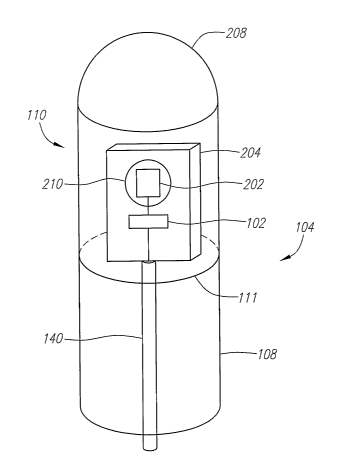
FIG: '2 Ys-=a pt~'rs~~cti~~ vievt~'d'dp7d~in~ a CMUT array 202 integrated with
bias circuitry 102 on
a common semiconductor substrate 204, such as Silicon, Gallium Arsenide (GaAs)
and the
like. The integrated CMUT array 202 and bias circuitry 102 are located within
housing 208
and mounted on the distal end 111 of driveshaft 108. Housing 208 preferably
includes an
imaging window 210, which can be either an open portion of the housing 208 or
a window
formed from a material that does not significantly impede the transmission or
reception of
ultrasound signals. Although not depicted here, the integrated CMUT array 202
and bias
circuitry 102 can be packaged using any desired packaging technique in order
to provide
protection, ease of mounting within housing 208 or for any other desired
purpose.
As mentioned above, CMUTs 101 are typically fabricated using semiconductor-
based
manufacturing processes on a semiconductor substrate 204. Preferably, the bias
circuitry 102 is
integrally fabricated on the same substrate 204 as the C1V1UT 101. CMUT 101
and bias
circuitry 102 can be fabricated using the same process flow or in different
process flows. In
embodiments having a CMUT array 202, bias circuitry 101 can be configured to
bias each
individual C1VITJT 101 in the array 202 or multiple bias circuits 101 can be
provided to bias
each CMUT separately. The integration of bias circuitry 102 with CMUT 101
allows for
improved performance of the imaging device 110 while at the same time making
fabrication of
the imaging device easier and less costly. Although integration of C1V1UT 101
and bias
circuitry 102 on common substrate 204 is preferred, it should be understood
that the systems
and methods described herein are not limited to such. For instance, CMUT 101
and bias
circuitry 102 can be fabricated as discrete components and packaged together,
or fabricated and
packaged discretely. Furthermore, CMUT 101 and bias circuitry 102 are not
required to be
housed together within housing 208, and in fact can be positioned in any
desired location
within catheter 104.
FIGs. 3A-B are cross-sectional views depicting an example embodiment of a CMUT
101. FIG. 3A depicts an unbiased CMUT 101 having a flexible upper electrode
302 suspended
over a lower electrode 304 both of which are fabricated on substrate 204. The
flexible upper
electrode 302 is also referred to in some contexts as a "drumhead." Located
between electrodes
302 and 304 is an insulator layer 306, composed of an insulating material such
as silicon oxide
or the like. Preferably, upper electrode 302 and lower electrode 304 are
separated by a gap 308.
Upper electrode 302 can completely encase gap 308 on all sides, in which case
gap 308 is
preferably a vacuum.
FIG. 3B depicts CMUT 101 after a DC bias voltage 310 is applied across
electrodes
302 and 304. DC bias voltage 310 builds a capacitive charge on the electrodes
302 and 304
-5-
CA 02583661 2007-04-12
WO 2006/044563 PCT/US2005/036868
d'ausihg uppbY'el'dbt.rertld MV-401TteX-1,1 or aenect, downwards towards lower
electrode 304 in
direction 312. The application of a drive signal, such as an electrical pulse
or an AC signal, to
the biased CMUT 101 modulates the degree of deflection of upper electrode 302
causing the
generation of an ultrasound pulse, which can be used to image body tissue.
Conversely, when
an ultrasound pulse, such as a received echo, impacts the biased CMUT 101, an
electrical pulse
corresponding to the strength of the received echo is generated. In this
manner, CMUT 101 can
be used to transmit and receive ultrasound signals in IVUS imaging system 100.
The actual DC bias voltage 310 and drive signal levels are dependent on the
needs of
the application and the characteristics of each CMUT 101. In general, a larger
DC bias voltage
310 will translate into the generation of a stronger ultrasound pulse. In
addition, the bias
voltage 310 can also be a factor in determining the frequency of the generated
ultrasound pulse.
In some applications, the DC bias voltage 310 can be approximately 100-150
volts, while the
drive signal level can be 75 volts or more. It should be understood that these
values are
provided solely as examples and any signal levels can be used as desired.
The design and fabrication of CMUT devices is discussed further in Percin, G.
and B.
Khuri-Yakub, Piezoelectrically actuated flextensional naicromachined ultt
asound transducers,
Ultrasonics, 2002. 40(1-8): p. 441-8, Percin, G. and B. Khuri-Yakub,
Piezoelectrically actuated
flextensioiaal micramachined ultrasound transducers--II.= fabrication and
experiments, IEEE
Trans Ultrason Ferroelectr Freq Control, 2002. 49(5): p. 585-95 and Percin, G.
and B. Khuri-
Yakub, Piezoelectrically actuated flextensional micYomachined ultrasound
transduceNs--I.=
theory, IEEE Trans Ultrason Ferroelectr Freq Control, 2002. 49(5): p. 573-84,
each of which is
fully incorporated by reference herein.
FIG. 4 depicts another example embodiment of imaging device 110. In this
embodiment, imaging device 110 includes CMUT array 202, bias circuitry 102 and
rectification circuit 402, all of which are preferably integrated on common
substrate 204. Bias
circuitry 102 includes a signal blocking circuit 404 and a charge pump 406
configured to apply
the DC bias voltage 310 to the array 202. A bias signal is preferably
transmitted along
communication channel 140 to supply charge to charge pump 404 and generate the
DC bias
voltage level 310 necessary to properly bias the CMUTs 101 within array 202.
The design and
implementation of charge pumps are well known to those of skill in the art and
any type of
charge pump can be used. The charge pump preferably includes a charge storage
unit, such as
a switched capacitor bank and the like. Furthermore, DC bias circuitry 102 can
be any circuitry
configured to control and apply a DC bias voltage including, but not limited
to, a charge pump
404.
-6-
CA 02583661 2007-04-12
WO 2006/044563 PCT/US2005/036868
lx1 eri7'UotxiMents wnere Doupfirig aevice 130 uses an inductive or other non-
physical
electrical coupling to transfer AC signals between image processing system 120
and imaging
device 110, the bias signal is preferably a series of DC pulses that appear as
an AC signal to the
coupling device 130. In embodiments where coupling device 130 uses a physical
coupling,
such as a brush/contact combination, the bias signal can be a pure DC signal
if desired.
Rectification circuit 402 can be used to isolate the charge built up within
imaging
device 110. Because system 100 can be used primarily for medical imaging
within living
beings, rectification circuit 402 guards against the risk of electrical shock
or other hazards to
the patient or the circuitry of system 100. Specifically, rectification 402
can be used to block or
prevent signals, such as the charge in charge pump 406 or array 202, from
propagating onto
communication channel 140. Any type of rectification circuitry can be used,
such as one or
more diodes and the like. Signal blocking circuit 404 can be used to block the
CMUT drive
signal from propagating to charge pump 406. One of skill in the art will
readily recognize that
FIG. 4 depicts one of many possible different circuit layouts for imaging
device 110 and,
accordingly, the systems and methods described herein are not limited to any
one layout or
circuit design.
Communication channel 140 can include any number of signal lines or
transmission
lines as needed. For example, communication channel can include a ground
signal line, a
CMUT drive signal line and a bias circuitry bias signal line. However, because
system 100 is
preferably used for intravascular applications, the width of catheter 104 can
be a liniiting factor
preventing advancement through narrow vasculature. Thus, because each
additional signal line
generally adds width to the driveshaft 108, even if the driveshaft 108 itself
is used as a signal
line, the number of signal lines used in communication channel 140 is
preferably minimized.
Typical IVLJS imaging systems use a communication channel 140 that includes
two signal lines
which can be used to transfer single-ended or differential signals.
In order to use two signal lines to transfer the transducer drive signal, the
bias signal
and the transducer output signal, the systems and methods described herein use
a segmented
timing regime. FIG. 5 is a timing diagram depicting the signals output from
image processing
system 120 according to one example embodiment of the segmented timing regime.
In this
embodiment, imaging device 110 is rotated to image a cross-section of the body
lumen. The
transmission of an ultrasound pulse followed by the reception of the resulting
echo signals is
referred to herein as an imaging cycle. System 100 can be configured to
perform a
predetermined number of imaging cycles for every rotation, with each imaging
cycle being
performed at a separate angular location, or range of angular locations. For
instance, in one
-7-
CA 02583661 2007-04-12
WO 2006/044563 PCT/US2005/036868
'einF36di'rrieri'C;'iriidgimg,t3ev2'c'b,'Y'li;c1llpert,nrms 360 imaging cycles
in each rotation, with one
imaging cycle being performed at an angular location located one degree apart.
Preferably, imaging device 110 is rotated at a rate such that the time
required to perform
an imaging cycle is less than the time required to rotate the imaging device
110 from one
angular location to the next. For example, in FIG. 5, at time To the imaging
device 110 is at a
first angular location and at time T4 the imaging device 110 has been rotated
to a second
angular position. The imaging cycle for the first angular location occurs
between times To and
T2. More specifically, the CMUT drive signal 502 is transmitted from image
processing system
120 to the array 202 from time To to time Tl in order to cause each individual
CMUT 101 to
transmit an ultrasound pulse. From time Tl to time T2, image processing system
120 is in a
receiving period 502 awaiting any output signals generated by the array 202 in
response to
received echoes. This leaves the remaining time from T2 to T4 unused in any
imaging cycle.
During the time from T2 to T3, the image processing system 120 preferably
transmits
the bias signal 504 to bias circuitry 102. At time T4, the image processing
system 120 transmits
another drive signal 501 to initiate the imaging cycle at the next angular
location. In one
example embodiment, the time period from To to T4 is 130 microseconds, with
the time period
from To to Tl being approximately 50 nanoseconds, the time period from Tl to
T2 being
approximately 20 microseconds and the time period from T2 to T3 being
approximately 100
microseconds. These times are included as examples only and in no way limit
the systems and
methods described herein.
Bias circuitry 102 can use the bias signal to generate the required DC bias
voltage 310.
The amplitude of the bias signal 504 is preferably lower than the CMUT 101
excitement
threshold where the CMUT 101 produces an ultrasound pulse. In some
applications, small
ultrasound pulses may be tolerable if, for instance, the small ultrasound
pulse does not interfere
with the subsequent imaging cycle. The term "excitement threshold" as used
herein, refers to
the signal level which causes one or more transducers to generate ultrasound
pulses at a level
sufficient to interfere with an imaging cycle. In one embodiment, the
excitement threshold can
be 75 volts and the bias signal 504 is maintained at 70 volts, while the drive
signal 501 is 125
volts. These values are solely for example and in no way limit the systems and
methods
described herein. As mentioned above, the bias signal can be a series of DC
pulses instead of a
continuous DC pulse in order to propagate through coupling device 130, if
needed. Also, it
should be understood that any waveforms can be used for drive signal 501 and
bias signal 504.
The generation of bias signal 504 and drive signal 501, as well as the proper
timing for
doing so, can be controlled by the image processing system 120. Preferably,
the bias circuitry
-8-
CA 02583661 2007-04-12
WO 2006/044563 PCT/US2005/036868
102'N up so that the bias signal 504 does not cause bias
circuitry 102 to apply a DC bias voltage 310 that is too high. This can be
performed through
charge limiting circuitry well known to those of skill in the art. Also, in
certain applications,
multiple charging cycles may be needed before bias circuitry 102 can apply the
proper DC bias
voltage 310. Alternatively, in another embodiment the image processing system
120 can be
configured to output the bias signal prior to the commencement of imaging in
order to charge
up, or initialize, the bias circuitry 102. In this embodiment, the length of
the initialization
period can be as long as needed to charge the bias circuitry 102. Preferably,
the bias circuitry
102 is designed to be low leakage so that once the proper DC bias voltage 310
is reached,
minimal subsequent charging is needed.
FIG. 6 is a flow chart depicting a method 600 of operating the imaging device
110 with
an image processing system 120 in an embodiment where communication channel
140 has only
two signal lines available. At 604, the imaging device 110 is rotated to a
first angular location.
At 606, the image processing system 120 outputs a transducer drive signal 501
during a first
time period to cause one or more CMUTs 101 to generate an ultrasound pulse. At
608, the
image processing system 120 listens for any transducer output signals
representative of the
strength of an echo received by any CMUT 101 during a second time period. At
610, the
image processing system 120 outputs a bias signal 504 during a third time
period to charge the
bias circuitry 102.
In addition, method 600 can also include an optional initialization process,
referenced
as 602, where the image processing system 120 can output bias signal 504
during a fourth time
period, preferably in order to initialize the bias circuitry 102. Then, the
method returns to step
604 and rotates to the next angular position and repeats steps 606-610. This
process continues
until imaging at all of the desired angular locations has taken place. The
rotation of imaging
device is preferably continuous but performed at such a rate where the
rotation that occurs
during the imaging cycle is negligible for the needs of the application.
In the foregoing specification, the invention has been described with
reference to
specific embodiments thereof. It will, however, be evident that various
modifications and
changes may be made thereto without departing from the broader spirit and
scope of the
invention. For example, each feature of one embodiment can be mixed and
matched with other
features shown in other embodiments, and the sequence of steps shown in a
flowchart may be
changed. Features and processes known to those of ordinary skill may similarly
be
incorporated as desired. Additionally and obviously, features may be added or
subtracted as
-9-
CA 02583661 2007-04-12
WO 2006/044563 PCT/US2005/036868
desftd: tAcz'oidiiYgly; theliiMt7un i~s' not to be restricted except in light
of the attached claims
and their equivalents.
-10-