Note: Descriptions are shown in the official language in which they were submitted.
CA 02583683 2007-04-12
DESCRIPTION
Surface Reconstruction Method for Silicon Carbide Substrate
Technical Field
The present invention relates to a surface reconstruction method for a silicon
carbide substrate. In particular, the invention relates to a surface
reconstruction
method for a silicon carbide substrate that can more simply close micropipes
in a surface
of the silicon carbide substrate.
Background Art
Silicon carbide (SiC) has a band gap approximately three times wider, a
breakdown voltage approximately ten times higher, a saturated electron drift
velocity
approximately twice higher, and a thermal conductivity approximately three
times higher,
than those of silicon (Si), and thus silicon carbide has the characteristics
that are not in
silicon. Further, silicon carbide is a thermally and chemically stable
semiconductor
material. Therefore, it is expected that a device using a silicon carbide
substrate is
employed as a power device that surmounts physical limitations of a device
using silicon
or as an environment-resistant device operating at high temperatures.
For optical devices, a material development of gallium nitride (GaN) aiming at
shorter wavelengths is studied. The lattic~'mismatch of silicon carbide with
respect to
gallium nitride is significantly smaller than those of other compound
semiconductors.
Therefore, a silicon carbide substrate is of interest as a substrate for
epitaxial growth of
gallium nitride.
Such a silicon carbide substrate can be obtained by slicing, to a
predetermined
thickness, a single crystal silicon carbide manufactured for example by the
modified Lely
method. The modified Lely method is the method according to which a crucible
made
of graphite is provided in which a seed crystal substrate of single crystal
silicon carbide
is disposed in an upper portion of the crucible and silicon carbide crystal
powder is
-1-
CA 02583683 2007-04-12
contained in a lower portion thereof, an inert-gas atmosphere is provided
inside the
crucible, thereafter the silicon carbide crystal powder is heated to sublime
the silicon
carbide crystal powder, the vapor resultant from the sublimation is diffused
in the inert
gas, transported to a region near the seed crystal substrate and
recrystallized near the
surface of the seed crystal substrate set at a low temperature, and the single
crystal
silicon carbide is grown on the surface of the seed crystal substrate.
The silicon carbide substrate thus obtained using the modified Lely method,
however, has a problem of generatin-g many micropipes that have openings in a
surface
of the silicon carbide substrate and are hollow crystal defects extending in
the direction
of the c-axis.
Accordingly, Japanese Patent Laying-Open No. 2004-292305 (Patent Document
1) for example discloses a method according to which a seed crystal substrate
of single
crystal silicon carbide and a polycrystalline silicon carbide substrate are
laid on each
other with a silicon source therebetween, they are contained in an airtight
container,
thereafter the seed crystal substrate and the polycrystalline silicon carbide
substrate are
heated to 1400 C to 2300 C, the silicon source between the substrates is
melted into a
ultrathin silicon melt that is present between the substrates, and single
crystal silicon
carbide is grown on the seed crystal substrate by liquid phase epitaxial
growth. The
resultant micropipe density is 1/cm2 or less.
According to this method, in the heating to 1400 C to 2300 C, the silicon
melt,
which enters the portion between the seed crystal substrate and the
polycrystalline
silicon carbide substrate located on the seed crystal substrate, forms a
silicon melt layer
of approximately 30 m to 50 m in thickness at the interface between these
substrates.
The silicon melt layer becomes thinner as the heating temperature rises to
finally become
approximately 30 m in thickness. Then, carbon atoms flowing out from the
polycrystalline silicon carbide substrate are supplied through the silicon
melt layer onto
the seed crystal substrate, and the single crystal silicon carbide is grown on
the seed
crystal substrate by liquid phase epitaxial growth. It is disclosed that, in a
surface of
-2-
CA 02583683 2007-04-12
the liquid-phase epitaxially grown single crystal silicon carbide, the
micropipe defect
density is 1/cm2 or less.
Patent Document 1: Japanese Patent Laying-Open No. 2004-292305
Disclosure of the Invention
Problems to be Solved by the Invention
Regarding the method disclosed in Patent Document 1, however, it is difficult
to
control impurities for crystal growth in liquid phase, and a problem here is
that it is
impossible to form or keep an ultralow concentration layer, which is necessary
for the
high breakdown voltage device and in which mixture of impurities is hindered
to an
extreme degree. According to this method, it is necessary to separately
prepare the
seed crystal substrate, the polycrystalline silicon carbide substrate, the
silicon source and
the closed container for example and contain the seed crystal substrate and
the
polycrystalline silicon carbide substrate in the closed container in the state
where the
substrates are laid on each other with the silicon source therebetween, and a
problem
here is that the preparation itself entails considerable work. Further,
according to this
method, it is necessary to liquid-phase epitaxially grow the single crystal
silicon carbide
in the state where the silicon melt layer on the surface of the seed crystal
substrate is
present between the substrates, and thus a problem here is that the silicon
melt layer is
difficult to control and considerable time is required for the growth of the
single crystal
silicon carbide. Furthermore, while the single crystal silicon carbide is
grown, the
impurity concentration near the growth surface changes at any time and thus a
problem
here is that control of impurities is difficult.
In view of the above-described circumstances, an object of the present
invention
is to provide a surface reconstruction method for a silicon carbide substrate
that can
more simply close micropipes in a surface of the silicon carbide substrate
without
epitaxial growth of silicon carbide crystal on the surface of the silicon
carbide substrate.
Means for Solving the Problems
The present invention is a surface reconstruction method for a silicon carbide
-3-
CA 02583683 2007-04-12
substrate, including: a silicon film forming step of forming a silicon film on
a surface of
the silicon carbide substrate; and a heat treatment step of heat-treating the
silicon
carbide substrate and the silicon film without providing a polycrystalline
silicon carbide
substrate on a surface of the silicon film.
Here, preferably the surface reconstruction method for the silicon carbide
substrate according to the present invention includes the step of performing,
before
forming the silicon film, planarization by etching or polishing of the surface
of the silicon
carbide substrate.
Further, the surface reconstruction method for the silicon carbide substrate
according to the present invention may include a silicon film removal step of
removing
the silicon film after the heat treatment step.
Further, the surface reconstruction method for the silicon carbide substrate
according to the present invention may include a silicon oxide film forming
step of
oxidizing the silicon film after the heat treatment step to generate a silicon
oxide film,
and a silicon oxide film removal step of removing the silicon oxide film.
Further, according to the surface reconstruction method for the silicon
carbide
substrate of the present invention, the silicon film may be formed by
sputtering or vapor
deposition method.
Further, according to the surface reconstruction method for the silicon
carbide
substrate of the present invention, the silicon film may be formed by using a
liquid
containing silicon or a gas containing silicon. Here, the silicon film forming
step and
the heat treatment step may be performed simultaneously.
Further, according to the surface reconstruction method for the silicon
carbide
substrate of the present invention, the silicon film is preferably formed on
an off-plane of
the silicon carbide substrate.
Effects of the Invention
In accordance with the present invention, a surface reconstruction method for
a
silicon carbide substrate can be provided that can more simply close
micropipes in a
-4-
CA 02583683 2007-04-12
surface of the silicon carbide substrate.
Brief Description of the Drawings
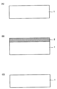
Fig. 1 is a schematic cross section diagrammatically showing a preferred
example
of a surface reconstruction method for a silicon carbide substrate according
to the
present invention.
Fig. 2 is a schematic cross section of an apparatus for forming a silicon film
used
in Example 3 of the present invention.
Fig. 3 is a schematic cross section of an apparatus for forming a silicon film
used
in Example 4 of the present invention.
Description of the Reference Signs
1 silicon carbide substrate, 2 silicon film, 11 substrate holder, 12 spray, 13
hexachlorodisilane, 14 gas supply pipe, 15 gas mixture, 16 vapor deposition
apparatus,
17 gas exhaust outlet
Best Modes for Carrying Out the Invention
In the following, an embodiment of the present invention is described. In the
drawings of the present application, the same reference characters represent
the same or
corresponding components.
In Fig. 1(A) to (C), a schematic cross section is shown that diagrammatically
shows a preferred example of a surface reconstruction method for a silicon
carbide
substrate according to the present invention. First, as shown in Fig. 1(A), a
silicon
carbide substrate 1 is prepared. Here, silicon carbide substrate 1 may be
obtained by
slicing, to a predetermined thickness, a silicon carbide crystal produced for
example by
the modified Lely method, may be obtained by using a commercially available
silicon
carbide substrate, or may be obtained by growing a silicon carbide crystal on
any
substrate. In other words, the silicon carbide substrate used in the present
invention is
not particularly limited as long as the substrate has a surface made of
silicon carbide
crystal.
Next, as shown in Fig. 1(B), a silicon film 2 is formed on this silicon
carbide
-5-
CA 02583683 2007-04-12
substrate 1. Without providing a polycrystalline silicon carbide substrate on
the surface
of the silicon film, silicon carbide substrate 1 is heat-treated so that
micropipes occurring
in silicon carbide substrate 1 can be closed. A reason why the micropipes can
be
closed by the present invention is supposed to be as follows. Silicon film 2
is formed
on silicon carbide substrate 1, silicon carbide substrate 1 and silicon film 2
are heat-
treated without providing a polycrystalline silicon carbide substrate on the
surface of
silicon film 2 and accordingly, into openings of micropipes in the surface of
silicon
carbide substrate 1, carbon atoms are supplied from only silicon carbide
substrate 1
without excessive supply of carbon atoms from the outside. Further, silicon
atoms are
supplied into the openings from silicon film 2. Thus, the surface of silicon
carbide
substrate 1 is reconstructed to close openings of micropipes without epitaxial
growth of
single crystal silicon carbide.
To begin with, micropipes are likely to occur in such crystal growth through a
rare layer as sublimation and vapor deposition under the conditions that the
temperature
is high, the surface is in disordered state and energy is stable. The heating
after silicon
film 2 is formed allows an excessive quantity of silicon atoms to be supplied
from silicon
film 2 to the surface of silicon carbide substrate 1, so that transport of
atoms at the
interface between silicon carbide substrate 1 and silicon film 2 can be
promoted. In a
low-temperature state after the heating, kinks are relatively few in the
surface and the
arranged and flat surface becomes stable. It is supposed that, for this
reason, the
surface is reconstructed to close micropipes.
Here, silicon film 2 can be formed easily on silicon carbide substrate 1 by
using,
for example, sputtering or vapor deposition. Further, silicon film 2 can also
be formed
by spraying an atomized liquid containing silicon (Si2Cl6 for example) onto
the top of
silicon carbide substrate 1 while silicon carbide substrate I is heat-treated.
Furthermore, silicon film 2 can also be formed by allowing a gas containing
silicon
(SiH2C12 or SiC14 for example) to contact the top of silicon carbide substrate
1 while
silicon carbide substrate 1 is heat-treated. Thus, by spraying a liquid
containing silicon
-6-
CA 02583683 2007-04-12
onto the top of silicon carbide substrate 1 which is being heat-treated, or
allowing a gas
containing silicon to contact the top of silicon carbide substrate 1 which is
being heat-
treated, the formation of silicon film 2 and the heat treatment of silicon
carbide substrate
1 and silicon film 2 can be carried out simultaneously.
The thickness of silicon film 2 formed on silicon carbide substrate 1 may be
for
example at least 10 nm and at most 1 m. The temperature at which silicon
carbide
substrate 1 and silicon film 2 are heat-treated may be, for example, at least
1300 C and
at most 1800 C.
According to the present invention, prior to the formation of silicon film 2,
preferably the step is included of planarizing the surface of silicon carbide
substrate 1 by
etching or polishing the surface. In the case where any flaws remain in the
surface of
silicon carbide substrate 1, remedy of defects is hindered. Therefore,
preferably the
planarization is performed to remove flaws in the surface of silicon carbide
substrate 1.
Here, the etching can be accomplished by, for example, exposing the surface of
silicon carbide substrate 1 to hydrogen or HCl and heating it to a temperature
of at least
1300 C. Further, the polishing can be accomplished by, for example, CMP
(Chemical
Mechanical Polishing).
Preferably, silicon film 2 is formed on an off-plane of silicon carbide
substrate 1
which is hexagonal crystal. Here, the off-plane may be formed as a plane
inclined with
respect to the (0001) plane of hexagonal silicon carbide substrate 1 by 8 for
example in
the [11-20] direction or [1-100] direction. Generally, in the case where the
off-plane
of the (0001) plane of hexagonal silicon carbide substrate I is not formed,
there is.the
tendency that a silicon carbide crystal is not grown on the (0001) plane of
silicon carbide
substrate 1 due to formation of a bicrystal. In contrast, in the case where
the off-plane
is formed as described above, there is the tendency that, as no bicrystal is
formed, a
silicon carbide crystal can be grown on the off-plane of silicon carbide
substrate 1.
Thus, in the case where the silicon film is formed on the off-plane of
hexagonal silicon
carbide substrate 1, when the silicon film is removed after heat treatment of
silicon
-7-
CA 02583683 2007-04-12
carbide substrate I and silicon film 2, the off-plane of silicon carbide
substrate 1 with
reduced micropipes can be obtained. Therefore, in the case where this silicon
carbide
substrate 1 is thereafter used as a substrate for example of a device, there
is the tendency
that a good-quality silicon carbide crystal can be grown on the surface of the
substrate.
Finally, as shown in Fig. 1 (C), silicon film 2 on silicon carbide substrate 1
is
removed for example by chemical etching with a liquid mixture of hydrofluoric
acid and
nitric acid for example. Accordingly, silicon carbide substrate 1 with closed
micropipes
can be obtained. Moreover, according to the present invention, silicon film 2
on silicon '
carbide substrate 1 may be heated for example in an oxygen atmosphere to
generate a
silicon oxide film and the silicon oxide film may be chemically etched with
hydrofluoric
acid for example to remove the silicon oxide film.
Examples
Example 1
First, a silicon carbide substrate made of a commercially available hexagonal
silicon carbide crystal and in the shape of a disk with a diameter of two
inches was
prepared. For an off-plane inclined by 8 in the [11-20] direction with
respect to the
(0001) plane of the surface of the silicon carbide substrate, the micropipe
density
(number of micropipes/cmZ) was checked by a method using light scattering to
find that
the micropipe density was 96 (micropipes/cm2).
Next, on the off-plane of the silicon carbide substrate, a silicon film was
formed
by sputtering to a thickness of 100 nm. Then, in a heat-treatment furnace of
an argon
gas atmosphere at a pressure of 1 x 10⁵ Pa, the silicon carbide substrate and
the silicon
film were heat-treated at 1500 C.
Finally, the silicon film was removed by means of a liquid mixture of
hydrofluoric
acid and nitric acid. The micropipe density of the off-plane of the silicon
carbide
substrate from which the silicon film had been removed was checked by the same
method as the above-described one. The density decreased to 12
(micropipes/cmZ).
Closed micropipes were examined to confirm that the micropipes were closed
-8-
CA 02583683 2007-04-12
with silicon carbide.
Example 2
First, as Example 1, a silicon carbide substrate made of a commercially
available
hexagonal silicon carbide crystal and in the shape of a disk with a diameter
of two inches
was prepared. For an off-plane inclined by 8 in the [11-20] direction with
respect to
the (0001) plane of the surface of the silicon carbide substrate, the
micropipe density
(number of micropipes/cm2) was checked by the same method as that of Example 1
to
find that the micropipe density was 92 (micropipes/cm2).
Next, on the off-plane of the silicon carbide substrate, a silicon film was
formed
by sputtering to a thickness of 100 nm as Example 1. Then, in a heat-treatment
furnace
of an argon gas atmosphere at a pressure of 1 x 10⁵ Pa, the silicon carbide
substrate and
the silicon film were heat-treated at 1500 C.
Subsequently, in a heat-treatment furnace of an oxygen atmosphere at a
pressure
of 1 x 10⁵ Pa, the silicon carbide substrate and the silicon film were heat-
treated at
1300 C to produce a silicon oxide film from the silicon film on the silicon
carbide
substrate. Finally, the silicon oxide film was removed by means of
hydrofluoric acid.
The micropipe density of the off-plane of the silicon carbide substrate from
which the
silicon oxide film had been removed was checked by the same method as the
above-
described one. The density decreased to 8(micropipes/cm).
Example 3
First, as Example 1, a silicon carbide substrate made of a commercially
available
hexagonal silicon carbide crystal and in the shape of a disk with a diameter
of two inches
was prepared. For an off-plane inclined by 8 in the [11-20] direction with
respect to
the (0001) plane of the surface of the silicon carbide substrate, the
micropipe density
(number of micropipes/cmZ) was checked by the same method as that of Example I
to
find that the micropipe density was 95 (micropipes/cm2).
Next, as shown in the schematic cross section of Fig. 2, onto the off-plane of
silicon carbide substrate 1 mounted on a substrate holder 11 and heated to
1500 C in an
-9-
CA 02583683 2007-04-12
argon gas atmosphere at a pressure of 1 x 10⁵ Pa, a liquid hexachlorodisilane
(SizCl6) 13
as atomized was sprayed from a spray 12. Thus, on the off-plane of silicon
carbide
substrate 1, hexachlorodisilane 13 was thermally decomposed to form a silicon
film on
the off-plane of silicon carbide substrate 1 and, simultaneously, silicon
carbide substrate
1 and the silicon film were heat-treated. After this, the spray of
hexachlorodisilane 13
and the heat treatment of silicon carbide substrate 1 and the silicon film
were stopped.
Finally, the silicon film formed on the off-plane of silicon carbide substrate
1 was
removed by means of a liquid mixture of hydrofluoric acid and nitric acid. The
micropipe density of the off-plane of the silicon carbide substrate from which
the silicon
film had been removed was checked by the same method as the above-described
one.
The density decreased to 11 (micropipes/cm).
Example 4
First, as Example 1, a silicon carbide substrate made of a commercially
available
hexagonal silicon carbide crystal and in the shape of a disk with a diameter
of two inches
was prepared. For an off-plane inclined by 8 in the [11-20] direction with
respect to
the (0001) plane of the surface of the silicon carbide substrate, the
micropipe density
(number of micropipes/cm2) was checked by the same method as that of Example 1
to
find that the micropipe density was 91 (micropipes/cm2).
Next, as shown in the schematic cross section of Fig. 3, a gas mixture 15 of
tetrachlorosilane (SiCl4) gas and hydrogen gas which is carrier gas was
supplied from a
gas supply pipe 14 into a vapor deposition apparatus 16 so that the gas
mixture
contacted the off-plane of silicon carbide substrate 1 that was mounted on
substrate
holder 11 and heated to 1300 C. In this way, on the off-plane of silicon
carbide
substrate 1, the tetrachlorosilane gas and the hydrogen gas reacted with each
other to
form a silicon film on the off-plane of silicon carbide substrate I and
simultaneously,
silicon carbide substrate 1 and the silicon film were heat-treated. A portion
of gas
mixture 15 that was not used for the reaction as well as a gas generated from
the
reaction were discharged from a gas exhaust outlet 17.
-10-
CA 02583683 2007-04-12
Finally, the silicon film formed on the off-plane of silicon carbide substrate
1 was
removed by means of a liquid mixture of hydrofluoric acid and nitric acid. The
micropipe density of the off-plane of the silicon carbide substrate from which
the silicon
film had been removed was checked by the same method as the above-described
one.
The density decreased to 9(micropipes/cm2).
Example 5
First, a silicon carbide substrate made of a commercially available hexagonal
silicon carbide crystal and in the shape of a disk with a diameter of two
inches was
prepared. For an off-plane inclined by 8 in the [11-20] direction with
respect to the
(0001) plane of the surface of the silicon carbide substrate, the micropipe
density
(number of micropipes/cm2) was checked by a method using light scattering to
find that
the micropipe density was 96 (micropipes/cm2).
Next, the off-plane of the silicon carbide substrate was exposed to hydrogen
and
heated to 1300 C so as to etch and planarize the off-plane. After this, on the
planarized off-plane, a silicon film was formed by means of sputtering to a
thickness of
100 nm. Subsequently, in a heat-treatment furnace of an argon gas atmosphere
at a
pressure of 1 x 10⁵ Pa, the silicon carbide substrate and the silicon film
were heat-
treated at 1500 C.
Finally, the silicon film was removed by means of a liquid mixture of
hydrofluoric
acid and nitric acid. The micropipe density of the off-plane of the silicon
carbide
substrate from which the silicon film had been removed was checked by the same
method as the above-described one. The density decreased to 7(micropipes/cmZ).
Example 6
First, a silicon carbide substrate made of a commercially available hexagonal
silicon carbide crystal and in the shape of a disk with a diameter of two
inches was
prepared. For an off-plane inclined by 8 in the [11-20] direction with
respect to the
(0001) plane of the surface of the silicon carbide substrate, the micropipe
density
(number of micropipes/cm2) was checked by a method using light scattering to
find that
-11-
CA 02583683 2007-04-12
the micropipe density was 94 (micropipes/cm2).
Next, the off-plane of the silicon carbide substrate was planarized by CMP.
After this, on this off-plane, a silicon film was formed by means of
sputtering to a
thickness of 100 nm. Subsequently, in a heat-treatment furnace of an argon gas
atmosphere at a pressure of 1 x 10⁵ Pa, the silicon carbide substrate and the
silicon film
were heat-treated at 1500 C.
Finally, the silicon film was removed by means of a liquid mixture of
hydrofluoric
acid and nitric acid. The micropipe density of the off-plane of the silicon
carbide
substrate from which the silicon film had been removed was checked by the same
method as the above-described one. The density decreased to 4(micropipes/cm).
The embodiments and examples herein disclosed are by way of illustration and
example in every respect, and are not to be taken by way of limitation. The
scope of
the present invention is not shown by the description above but by claims, and
it is
intended that all modifications are included within the meaning and scope
equivalent to
the claims.
Industrial Applicability
In accordance with the present invention, micropipes in a surface of a silicon
carbide substrate can more simply be closed without work and time necessary
for such a
conventional method as the one using liquid phase epitaxial growth and
accordingly, a
good-quality silicon carbide substrate with few surface defects can be
obtained.
As seen from the above, the silicon carbide substrate obtained according to
the
present invention can suitably be used for, for example, a power device,
environment-
resistant device operating at high temperatures or optical device.
-12-