Note: Descriptions are shown in the official language in which they were submitted.
CA 02583760 2007-04-13
METHOD FOR CONTACT SEPARATION OF ELECTRICALLY CONDUCTIVE
LAYERS ON BACK-CONTACTED SOLAR CELLS AND SOLAR CELL
The present invention relates to a solar cell in which both an emitter contact
and a
base contact are arranged on a back side of a semiconductor substrate and a
method for
fabricating such a solar cell. In particular, the invention relates to a
method for electrically
separating base and emitter contacts arranged on the back side of a solar
cell.
BACKGROUND OF THE INVENTION
Solar cells are used to convert light into electrical energy. In this case,
charge
carrier pairs generated by light in a semiconductor substrate are separated by
a pn junction
and then supplied via the emitter contact and the base contact to a power
circuit
comprising a consumer.
PRIOR ART
In conventional solar cells, the emitter contact is mostly arranged on the
front side,
i.e. on the side facing the light source, of the semiconductor substrate.
However, solar cells
have also been proposed, for example, in JP 5-75149 A, DE 41 43 083 and DE 101
42 481
in which both the base contact and also the emitter contact are arranged on
the back side of
the substrate. Firstly, this avoids shading of the front side by the contacts,
leading to
enhanced efficiency and improved aesthetics of the solar cell, and secondly,
these solar
cells are easier to connect in series since the back side of a cell need not
be electrically
connected to the front side of a neighbouring cell.
In other words, a solar cell without front-side metallisation has a plurality
of
advantages: the front side of the solar cell is not shaded by any contact so
that the incident
radiation energy can generate charge carriers in the semiconductor substrate
without
restriction. In addition, these cells can be easier to connect to modules and
they have good
aesthetics.
However, conventional so-called back-contact solar cells have several
disadvantages. Their fabrication methods are mostly elaborate. Some methods
require a
plurality of masking steps, a plurality of etching steps and/or a plurality of
vapour
deposition steps to form the base contact electrically separate from the
emitter contact on
the back side of the semiconductor substrate. Furthermore, conventional back-
contact
solar cells frequently suffer from local short circuits, caused for example by
inversion
layers between the base and the emitter region or by inadequate electrical
insulation
between the emitter and the base contact, leading to a reduced efficiency of
the solar cell.
CA 02583760 2008-01-09
A solar cell without front-side metallisation is known, for example, from R.
M.
Swanson "Point Contact Silicon Solar Cells", Electric Power Research Institute
Rep. AP-
2859, May 1983. This cell concept has been continuously further developed
(R.A.Sinton
"Bilevel contact solar cells", US Patent 5,053,083, 1991). A simplified
version of this
point contact solar cell is being manufactured by SunPowerCorporation in a
pilot line
(K.R. McInthosh, M. J. Cudzinovic, D-D Smith, W-P. Mulligan and R. M. Swanson
"The
choice of silicon wafer for the production of low-cost rear-contact solar
cells", 3rd World
Conference on PV Energy Conversion, Osaka 2003, in press).
For the fabrication of these solar cells, differently doped regions must be
produced
adjacent to one another in a plurality of masking steps and metallised or
contacted by
applying a partially multilayer metal structure.
A disadvantage here is these methods require a plurality of aligning masking
steps
and are therefore elaborate.
Known from JP 575149 A is a solar cell without front-side metallisation which
has
elevated and recessed regions on the back side of the solar cell. This solar
cell can also
only be fabricated using a plurality of masking and etching steps. In
addition, the
formation of elevated and recessed regions requires additional work steps
compared to a
solar cell with flat surfaces.
Patent DE 41 43 083 describes a solar cell without front-side metallisation in
which aligning masking steps are not absolutely necessary. However, the
efficiency of this
cell is low since the inversion layer connects two contact systems which
brings about a
low parallel resistance and therefore a low fill factor.
Patent DE 101 42 481 describes a solar cell with base and emitter contacts on
the
rear side. This solar cell also has a rear-side structure but the contacts are
located on the
flanks of the elevations. This requires two vacuum vapour deposition steps to
fabricate the
contacts. In addition, the fabrication of a local emitter is technologically
demanding in this
cell.
A particular difficulty with back-contacted solar cells is the elaborate
fabrication of
the back side contacts where electrical short circuits must be absolutely
avoided.
SUIMMARY OF THE INVENTION
There may be a need for the present invention to avoid or at least reduce the
aforesaid problems and to provide a solar cell and a method of fabrication for
a solar cell
which achieves a high efficiency and is easy to produce.
2
CA 02583760 2008-01-09
,
In one aspect, the present invention provides a method for fabricating a solar
cell
by providing a semiconductor substrate with a substrate front side and a
substrate back
side, forming an emitter region and a base region each on the substrate back
side; forming
an electrically insulating layer on the substrate back side at least in
junction regions above
a region boundary at which the emitter region adjoins the base region;
depositing a metal
layer at least on partial regions of the substrate back side; depositing an
etch barrier layer
at least on partial regions of the metal layer (the etch barrier layer being
substantially
resistant towards an etchant for etching the metal layer); locally removing
the etch barrier
layer at least in partial regions of the junction regions; and etching the
metal layer ( the
metal layer being substantially removed in the partial regions in which the
etch barrier
layer is locally removed).
In various aspects of the present invention, the method for fabricating a
solar cell
includes removing the etch barrier free from masking. Various aspects of the
invention
include methods to remove the etch barrier using a laser, a locally applied
etching
solution, or local mechanical removal.
In other embodiments of the invention, the etch barrier is locally removed in
a
region laterally spaced from the region boundary. The etch barrier is, in
various aspects of
the invention, electrically conductive and, optionally, can be soldered.
Embodiments of the present invention include depositing the etch barrier layer
and/or the metal layer by vapour deposition or by sputtering. Further aspects
of the
invention include methods that locally remove the etch-barrier layer in
meander-shaped
regions, and other aspects relate to methods where the etch barrier layer is
locally removed
in such a manner that elongated metallisation finger regions between regions
in which the
etch barrier layer is removed, taper from one side edge of the solar cell
towards an
opposite side edge.
The electrically insulating layer of various aspects of the invention can
comprise
silicon oxide and/or silicon nitride, and/or can be applied above the
electrically insulating
layer.
In a further embodiment, the present invention provides a solar cell
comprising a
semiconductor substrate having: a substrate front side and a substrate back
side; a base
region of a first doping type on the substrate back side and an emitter region
of a second
doping type on the substrate back side; a dielectric layer in junction regions
above a region
boundary at which the base region adjoins the emitter region; a base contact
which
electrically contacts the base region at least in partial regions, and an
emitter contact which
electrically contacts the emitter region at least in partial regions, wherein
the base contact
and the emitter contact each have a metal layer in contact with the
semiconductor
substrate, wherein the metal layer of the base contact is laterally spaced
apart from the
2a
CA 02583760 2008-01-09
,
metal layer of the emitter contact above the dielectric layer by a separating
gap so that the
emitter contact and the base contact are electrically separated, wherein the
solar cell
comprises a solderable etch barrier layer which covers the metal layers of the
base contact
and the emitter contact at least in part.
In another aspect of the present invention, the separating gap of the solar
cell is
laterally spaced apart from the region boundary at least in partial regions.
In further
embodiments of the present invention, the metal layer of the base contact and
the metal
layer of the emitter contact are arranged substantially at the same distance
from the
substrate front side.
The etch barrier layer in various aspects of the invention comprises silver
and/or
copper, and the metal layers of the emitter contact and/or the base contact
comprise
aluminium in various embodiments of the invention.
Various aspects of the solar cell of the present invention have an
electrically
insulating varnish layer which covers the dielectric layer at least partially,
and a variety of
embodiments have the separating gap is formed in a meander shape.
Finally, in a number of embodiments, the emitter contact and/or the base
contact
are formed with elongated fingers which taper from one side edge of the solar
cell to an
opposite side edge.
2b
CA 02583760 2007-04-13
In particular, the invention solves the problem of fabricating the two back-
side
contact systems i.e. base contact and emitter contact and their problem-free
electrical
separation in a simple manner and describes a solar cell which can be
fabricated simply by
this method.
DESCRIPTION OF THE INVENTION
According to a first aspect of the invention, a method for fabricating a solar
cell is
provided, comprising the following steps: providing a semiconductor substrate
with a
substrate front side and a substrate back side; forming an emitter region and
a base region
each on the substrate back side; forming an electrically insulating layer on
the substrate
back side at least in junction regions above a region boundary at which the
emitter region
adjoins the base region; depositing a metal layer at least on partial regions
of the substrate
back side; depositing an etch barrier layer at least on partial regions of the
metal layer,
wherein the etch barrier layer is substantially resistant towards an etchant
for etching the
metal layer; locally removing the etch barrier layer at least in partial
regions of the
junction regions; etching the metal layer, wherein the metal layer is
substantially removed
in the partial regions in which the etch barrier layer is locally removed.
A silicon wafer can be used as the semiconductor substrate. The method is
particularly suitable for the fabrication of back contact solar cells in which
an emitter is
formed both on the front and also on the back side of the solar cell (for
example, so-called
EWT (Emitter Wrap Through) solar cells). As a result of the short distance
from a pn
junction separating the charge carrier pairs, lower-quality silicon wafers,
for example,
made of multicrystalline silicon or Cz silicon, having a minority carrier
diffusion length
shorter than the thickness of the wafer, can be used in these solar cells.
Thin semiconductor layers applied to a carrier substrate having thicknesses in
the
range of a few micrometer can be used as the semiconductor substrate. The
method
according to the invention is particularly advantageous for the fabrication of
thin-layer
solar cells because, in contrast to some of the conventional methods specified
in the
introduction, no structuring of the substrate back side is required but the
method can be
applied to substrates with a flat back side.
The emitter region to be formed subsequently and the base region of the solar
cell
have different n-type or p-type dopings. The definition of the two regions can
be effected,
for example, by locally protecting the base layer from diffusion using a
masking layer or
by diffusion over the entire surface and subsequently locally etching away the
resulting
emitter or removing it by means of laser ablation. The two regions can be
nested in one
another in a comb-like fashion ("interdigitated"). This has the result that
charge carrier
pairs generated in the semiconductor substrate only have to travel short
distances up to a
3
CA 02583760 2007-04-13
pn junction and are then separated there and can be removed via the
metallisations
contacting the respective regions. Recombination and series resistance losses
can thus be
minimised. In this case, the emitter region and the base region do not need to
occupy the
same surface fractions on the entire back-side surface.
In the junction region above the region boundary at which the emitter region
adjoins the base region, i.e. at that point where a pn-junction reaches the
surface of the
substrate back side, an electrically insulating layer is formed on the
substrate back side.
"Above" is to be understood here as adjoining the surface of the substrate
back side.
"Junction regions" are understood as those regions which are laterally
adjacent to the
region boundary, i.e. parallel to the substrate surface.
The electrically insulating layer can be a dielectric which surface passivates
both
the substrate surface located thereunder and in particular the exposed pn-j
unction and also
prevents short circuits between the emitter region and the base region caused
by a metal
layer subsequently located thereover.
The insulating layer is preferably formed with silicon oxide and/or silicon
nitride.
This can be formed by means of any known method. For example, an oxide can be
grown
thermally on the silicon surface or a nitride can be deposited by means of a
CVD method.
In this case, it is important that the layer is electrically insulated as well
as possible. Any
pinholes can adversely affect the insulation properties of the layer. Thus,
care should be
taken to ensure that the layer is as compact as possible. Thermally grown
oxides are
usually more compact than deposited nitrides and may thus be preferable.
Since the insulating layer should only be formed in the junction regions, but
interlying regions should not be covered by the layer for purposes of
electrical contacting,
the insulating layer can be selectively applied through a mask, where
attention should be
paid to the correct positioning in relation to the region boundary.
Alternatively, the insulating layer can be formed over the entire area on the
back
side of the substrate and then removed locally, for example, in lines or
spots, by laser
ablation or local etching for example.
In another alternative, a masking layer which has been formed before in-
diffusion
of the emitter region on the base region in order to protect it from
diffusion, can remain on
the substrate back side and then serve as an insulating layer. Since emitter
dopants also
diffuse laterally under the masking layer during diffusion, this layer
subsequently covers
the region boundary between the emitter and base region.
In the next process step, a metal layer is preferably deposited on the entire
back
side of the substrate. Masking, for example, by photolithography, of
individual regions of
the substrate back side is not required. Partial regions of the substrate back
side, used for
4
CA 02583760 2007-04-13
example for holding the substrate during the deposition, possibly remain free
from the
metal layer. Aluminium is preferably used for the metal layer.
After the metal layer has been deposited, an etch barrier layer is deposited
on this,
again at least in partial regions. The etch barrier layer thus covers the
metall layer, at least
in part. Preferably both the metal layer and the etch barrier layer located
thereover
substantially cover the entire substrate back side.
According to the invention, the etch barrier layer is substantially resistant
to an
etchant used to etch the metal layer. This means that an etchant, for example,
a liquid
etching solution or a reactive gas which severely attacks the metal layer,
does not or only
1() slightly etches the etch barrier layer. For example, the etching rate
of the etchant relative
to the metal layer should be very much higher, for example, by a factor of
ten, than that
relative to the etch barrier layer.
Preferably conductive and, in particular, solderable metals such as silver or
copper
can be used for the etch barrier layer. The term "solderable" is understood
here in that a
conventional cable or a contact strip can be soldered onto the etch barrier
layer and this
can be used, for example, for connecting solar cells to one another. In this
case, it should
be possible to use simple, cost-effective soldering methods without using
special solders
or special tools such as are required to solder aluminium or titanium or
compounds of such
metals, for example. It should be possible to solder the etch barrier, for
example, using
conventional silver solder and conventional soldering irons.
However, dielectrics such as silicon oxide (e.g. Si02) or silicon nitride
(e.g. Si3N4)
can also be used and can possibly be used in subsequent fabrication steps for
contacting
the metal layer located thereunder.
The metal layer and/or the etch barrier layer are preferably deposited by
vapour
deposition or sputtering. Therein, both layers can by deposited during a
single vacuum
step.
The etch barrier layer is then removed locally at least in partial regions
above the
junction regions. In other words, the etch barrier layer is removed at least
in part, where
the substrate back side is covered by the electrically insulating layer at the
region
boundary of exposed pn junctions.
The etch barrier layer can preferably be removed free from masking, i.e. using
no
mask which has been laid on or generated photolithographically to locally open
the etch
barrier layer.
The etch barrier layer can preferably be locally removed by means of a laser
by
laser ablation. In this case, the etch barrier layer is locally vaporised by a
high-energy laser
or made to spall so that the metal layer located thereunder is exposed.
5
CA 02583760 2007-04-13
Alternatively, the etch barrier layer can be removed by means of an etching
solution which is applied locally for example, by a dispenser similar to an
ink jet printer.
In another alternative, the etch barrier layer can also be removed locally by
mechanical means, for example, by scoring or sawing.
In a subsequent process step, the back side of the substrate with the metal
layer
located thereon and the etch barrier layer covering this, is exposed to an
etchant. In the
regions covered by the etch barrier layer the metal layer is not attacked or
barely attacked
by the etchant. In the partial regions where the etch barrier layer has been
locally removed
however, the etchant can directly attack the metal layer. The metal layer
located under the
etch barrier layer is etched away in these partial regions. A separating
trench is formed,
which extends as far as the electrically insulating layer located thereunder.
As a result, the
metal layer in the base region is no longer electrically connected to the
metal layer in the
emitter region.
The method according to the invention can achieve electrical insulation of the
base
contact from the emitter contact also located on the back side of the
substrate in a simple
manner. In this context, it is advantageous that the electrically insulating
layer must cover
the region boundary at all points but can also extend over substantially
further regions of
the substrate back side. A dielectric acting as an insulating layer can
surface-passivate
broad areas of the back surface of the substrate and must only be locally
opened for
contacting the emitter. The base contacts can be driven through the dielectric
into the base
region by an LFC method (laser fired contacts). Alternatively, the dielectric
can be
selectively locally opened prior to the metal deposition in the base region.
The local removal of the etch barrier layer must again lie merely somewhere in
the
area of the underlying junction regions and take place such that after the
etching step, the
entire base contact is completely electrically separated from the emitter
contact. This
means that the separating trenches insulating the emitter contact from the
base contact
should always run in regions in which the adjoining metal layers are insulated
from the
substrate back side by the underlying insulating layer. If broad areas of the
substrate back
side are covered by the insulating layer, this therefore provides great
freedom with regard
to the geometrical profile of the separating trench. It need not be aligned
precisely above
the region boundary of the surface-pn-junctions but can run laterally spaced
apart from
this region boundary. For example, the separating trench can be formed as
meander-
shaped. It can also be formed in such a manner that elongated metallisation
finger regions
insulated from one another by the separating trench taper from one side edge
of the solar
cell towards an opposite side edge.
According to a second aspect of the present invention, a solar cell is
proposed,
comprising: a semiconductor substrate comprising a substrate front side and a
substrate
6
CA 02583760 2007-04-13
back side; a base region of a first doping type on the substrate back side and
an emitter
region of a second doping type on the substrate back side; a dielectric layer
in the junction
regions above a region boundary at which the base region adjoins the emitter
region; a
base contact which electrically contacts the base region at least in partial
regions and an
emitter contact which electrically contacts the emitter region at least in
partial regions,
wherein the base contact and the emitter contact each have a metal layer in
contact with
the semiconductor substrate, wherein the metal layer of the base contact is
laterally spaced
apart from the metal layer of the emitter contact above the dielectric layer
by a separating
gap so that the emitter contact and the base contact are electrically
separated.
In particular, the solar cell can have the features such as those formed by
the
method according to the invention described above.
In one embodiment, the solar cell is configured in such a manner that the
metal
layer of the base contact and the metal layer of the emitter contact are
arranged
substantially at the same distance from the substrate front side. In other
words, this means
that the two contacts are applied to a flat substrate back side. The contacts
are therefore
only separated laterally by a separating gap and there is no vertical spacing
such as can be
found in many conventional back-contact solar cells.
In a further embodiment, another thin metal layer is located above the metal
layer
forming the contacts, this thin layer serving as an etch barrier layer during
the fabrication
of the solar cell. This layer is preferably formed using a solderable material
such as, for
example, silver or copper. The contacts whose metal layer can be made of
difficult-to-
solder aluminium can be easily soldered with the aid of this layer and the
solar cells thus
interconnected to one another.
Further features and advantages of the invention are obtained from the
following
detailed description of preferred embodiments in connection with the
accompanying
drawings.
BRIEF DESCRIPTION OF THE DRAWINGS
Fig. 1 shows a schematic sectional view of a solar cell according to the
invention
according to a first embodiment.
Fig. 2A to 2C schematically illustrate process steps of a process sequence
according to the invention.
Fig. 3 shows a schematic sectional view of a solar cell according to the
invention
according to a second embodiment with separating trenches which are laterally
offset with
respect to a region boundary.
Fig. 4 shows a schematic view of a solar cell according to the invention
according
to a third embodiment in which the separating trench has a meander-shaped
configuration.
7
CA 02583760 2007-04-13
Fig. 5 shows a schematic view of a solar cell according to the invention
according
to a fourth embodiment with tapering contact fingers.
DESCRIPTION OF PREFERRED EMBODIMENTS
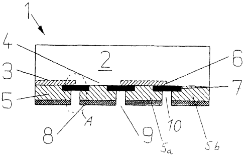
Embodiments of the solar cells 1 according to the invention and a method
according to the invention suitable for their fabrication are now described
with reference
to Figures 1, 2A to 2C and 3. Figures 2A to 2C illustrate the process steps
for separating
back-contact regions with reference to region A bordered by the dashed line in
Fig. 1.
On the back side of a p-doped silicon wafer serving as a semiconductor
substrate 2,
n-doped emitter regions 3 are diffused-in locally. For this purpose, the
surface of the
substrate 2 where no diffusion is to take place, is protected with a diffusion
barrier, for
example, silicon nitride and the substrate is then subjected to phosphorus
diffusion.
An electrically insulating layer 7 in the form of a thermally grown silicon
oxide
layer and a silicon nitride layer deposited over this by CVD is then applied
over the entire
back side of the substrate. This layer 7 is then removed locally in strips by
laser ablation in
the area of the subsequent emitter contacting, i.e. over the emitter region 3.
Then an
aluminium layer serving as a metal layer 5 is initially deposited over the
entire substrate
back side, making direct contact with the back side of the substrate in the
emitter region 3
whereas in the base region 4 and in a junction region adjacent to the region
boundary 6,
said layer is located above the insulating layer 7. In the same vapour
deposition step, a
silver layer serving as an etch barrier layer 8 is applied over the metal
layer 5. A sequence
of layers as shown in Fig. 2A is now provided.
Next, in a process step shown in Fig. 2B, the etch barrier layer 8 is locally
opened
using a laser. The geometry of the opened region 9 in which the etch barrier
layer 8 is
removed can be widely varied here. In order to prevent short circuits between
the
subsequent emitter contact and the subsequent base contact, it is merely
necessary to
ensure that the opened region 9 is already located above the insulating layer
7 and that an
opened region 9 is located above or adjacent to each region boundary 6.
As can be seen in the embodiment illustrated in Fig. 4, the opened region 9
can
have a meander-shaped profile. In this way, interdigitated contact fingers are
formed. In
another embodiment illustrated in Fig. 5, the interdigitated contact fingers
are configured
as tapered. This has the advantage that in regions of the contact fingers in
which a high
current flows, the cross-section of the contact fingers is large and thus
resistance losses are
reduced.
In a subsequent process step shown in Fig. 2C, the semiconductor substrate
with
the sequence of layers applied thereto is subjected to etching. In this case,
a solution, for
example, HC1-based or a reactive gas can be used as the etchant. This etchant
does not
8
CA 02583760 2007-04-13
attack or barely attacks the etching barrier. In the opened regions 9 however,
the etchant
acts directly on the metal layer 5 and etches it away. A separating trench 10
is formed,
which extends down to the insulating layer 7 and separates the metal layer 5a
of the
emitter contact from the metal layer 5b of the base contact.
Figure 3 shows an embodiment in which the separating trench 10 is located in a
region laterally at a distance from the region boundary 6. Furthermore, a
varnish layer 12
is applied locally over the insulating layer 7, increasing the resistance
between the metal
layer 5 and the underlying substrate. This can be particularly advantageous
when the
insulating layer 7 has microscopic pinholes which could cause short circuits.
To sum up and in other words, the invention can be described as follows: a
solar
cell (1) comprising a semiconductor substrate (2) is proposed where electrical
contacting
is made on the back side of the semiconductor substrate. The back side of the
semiconductor substrate has locally doped regions (3). The adjacent regions
(4) exhibit
different doping from the region (3). The two regions (3, 4) are initially
coated with
electrically conductive material (5) over the entire area. So that the
conductive material (5)
does not short-circuit the solar cell, the two regions (3, 4) are covered with
a thin
electrically insulating layer (7), at least at the region boundaries (6).
The electrically conductive layer (5) is separated by applying an etch barrier
layer
(8) over the entire surface which is then removed free from masking and
selectively e.g.
by laser ablation, locally below the insulating layer (7). The conductive
layer (5) is locally
removed in the area of the openings (9) of the etch barrier layer (8) by
subsequent action
of an etching solution.
The following advantages are achieved among others with the solar cell which
has
been presented, also designated as HORIZON cell (HOrizontal Rear
Interdigitated
ZONes):
Base and emitter back contacts electrically insulated from one another can
easily
be produced. The contacts have a double layer comprising a vapour-deposited
metal layer and an etch barrier layer. Contact separation is preferably
achieved by
means of non-contact local laser ablation or local etching away of the etch
barrier
layer and subsequent local etching away of the metal layer. No mechanical
loading
of the solar cell thus occurs during metallisation.
Only one vacuum deposition step is required for deposition of the metal layer
and
the etch barrier layer over the entire surface.
Metal contacts can be separated on a flat back side of the substrate; no
surface
structuring of the silicon wafer is required;
9
CA 02583760 2007-04-13
As a result of the flexible geometric configuration of the metal contacts, a
low
contact resistance and a low contact recombination as well as a high
conductivity
of the contact fingers can be achieved.
If a solderable etch barrier layer is used, this can be used simply by
soldering with
contact strips for connecting the solar cell to modules.
The solar cell according to the invention and the method of fabrication
according
to the invention have merely been described as examples by means of the above
embodiments. It is noted that the previously described process steps
principally relate to
the part of the complete processing of a solar cell which can be used
according to the
invention to form base and emitter back contacts electrically insulated from
one another. It
is clear to persons skilled in the art familiar with the prior art that the
process steps
described and changes and modifications which come within the scope of the
appended
claims can be combined with further known process steps and in this way,
various types of
solar cells can be produced. For example, various further steps such as, for
example,
surface texturing, emitter diffusion, surface passivation, deposition of an
anti-reflection
layer etc. can be used to form the front side of the solar cell.