Note: Descriptions are shown in the official language in which they were submitted.
CA 02583853 2007-04-04
-1-
TITLE: METHOD AND APPARATUS FOR TESTING SOLDERABILITY OF
ELECTRICAL COMPONENTS
TECHNICAL FIELD
[0001] The embodiments described herein relate generally to methods and
apparatuses for testing the solderability of electrical components, such as
surface mount components. In particular, the testing involves automated
measurement of surface tension in the solder when contacted with a surface of
the component.
BACKGROUND
[0002] Many small electronic components are mounted on Printed Circuit
Boards (PCB) using surface mount technology (SMT). These SMT components
are placed on the appropriate location on the PCB and are subsequently
soldered to the PCB by known processes. In order to determine the likelihood
of
failure of the solder connection between the SMT component and the PCB, it is
necessary to perform testing of the solderability of samples of the component.
[0003] Current instruments being used for solderability testing essentially
include analytical balances with a built-in clock poised over molten solder.
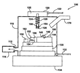
The
SMT component is suspended from the bottom of the balance prior to testing.
The SMT component has flux applied to it and is dipped into the molten solder.
The solder may be in a bath or formed as a small globule. The resulting
surface
tension of the molten solder wetting to the component is measured by the
analytical balance over a period of time. The resulting measurements are used
to plot a graph of the wetting force (i.e. the surface tension) versus time,
which is
then used to determine whether the component has suitable wetting properties
for providing good solderability. In order for the quality of solderability of
the
component to be considered adequate, the sample component must wet quickly
enough during the time that it is in contact with the molten solder and must
II
CA 02583853 2007-04-04
-2-
exhibit a wetting force large enough to provide a suitably sized solder fillet
in the
completed solder joint.
[0004] Where the testing uses small solder globules, and as available
solderability testing instrument pin sizes have decreased from a 4 mm diameter
to 1 mm, the limitations of the testing arrangements described above make it
difficult to accurately measure the wetting forces of the newest small
components. This is in part because of the smaller amounts of solder required
for the smaller pins. The sensitivity of the equipment used to measure the
wetting forces in such arrangements is inadequate for the smaller wetting
forces
required to be measured for the smaller SMT pin sizes. Some such
arrangements have a smallest full scale division of force measurement in
milliNewtons, which is inadequate to measure forces in the order of
microNewtons. The newly developed small pin sizes and smaller solder amounts
required for such pin sizes means that greater precision in force measurement
is
needed. However, when measuring such small forces, thermal currents in air at
standard pressure may be high enough relative to the small wetting forces that
unreliable results would be recorded or the test may be compromised.
[0005] Further, arrangements that rely on suspending a sample over
molten solder before contacting the solder suffer from non-uniform heating of
the
component sample. As the heating in a real reflow oven in the normal assembly
process is relatively uniform, it is desirable to mimic such conditions during
the
testing process, if possible. While the above described arrangements can
suspend the component sample over the molten solder for a period of time to
heat it prior to immersion in the solder, this generally does not result in
uniform
heating of the component sample.
[0006] It is desired to address or ameliorate one or more shortcomings or
disadvantages of prior methods and systems for testing the solderability of
surface mount components, or to at least provide a useful alternative thereto.
, ,, , õ
CA 02583853 2007-04-04
-3-
BRIEF DESCRIPTION OF THE DRAWINGS
[0007] Embodiments are described in further detail below, by way of
example only, with reference to the accompanying drawings, in which:
[0008] Figure 1 is a schematic front view of a solderability testing
apparatus according to one embodiment;
[0009] Figure 2 is a block diagram of a system for testing solderability,
including the apparatus of Figure 1; and
[0010] Figure 3 is a flow diagram of a method of measuring the
solderability of electrical components.
DETAILED DESCRIPTION
[0011] Embodiments described herein relate generally to methods and
apparatus for use in determining solderability of an electrical component. One
particular aspect relates to apparatus comprising a vacuum chamber, a load
sensor, a platform and a control module. The load sensor has a contact portion
disposed within the vacuum chamber. The platform is disposed within the
vacuum chamber in relation to the contact portion and has a component
mounting surface and a mounting member for mounting an electrical component
to the component mounting surface. The control module causes relative
movement between the platform and the load sensor so that a contact surface of
the electrical component is brought into close proximity with the contact
portion.
When the contact portion has solder thereon and the solder is brought into
contact with the contact surface, the load sensor measures force arising from
wetting of the solder to the contact surface. The force occurring under
contact
changes over time, depending on the degree of solderability of the electrical
component. Thus, measurement of the wetting forces over time provides an
indication of the solderability of the electrical component.
[0012] Providing a vacuum chamber in which the solderability testing can
be carried out allows for minimization of thermal currents that might cause
, ~, , õ
I ll
CA 02583853 2007-04-04
-4-
spurious results in the surface tension measurements. In one embodiment, a
load sensor having a measurement accuracy similar to that of an atomic force
microscope may be used. Such precision allows measurement of forces in the
order of microNewtons.
5[0013] In one embodiment, the apparatus comprises a first receptacle
containing solder, the first receptacle being positioned on the platform. A
first
heating element is associated with the first receptacle for heating the solder
in
the first receptacle. A first temperature sensor is also provided for sensing
a
temperature of the solder in the first receptacle.
[0014] In another embodiment, the apparatus further comprises a second
receptacle containing flux, the second receptacle being positioned on the
platform. The first and second receptacles have, in one embodiment, closable
openings arranged to be closed when the contact portion is not being dipped
into
the respective first or second receptacle. In another embodiment, a second
heating element is disposed on the platform. The second heating element has
an upper surface comprising the component mounting surface. The mounting
member is disposed on or adjacent the component mounting surface. A second
temperature sensor is provided for sensing a temperature of the second heating
element.
[0015] In one embodiment, the load sensor comprises a projection and the
contact portion is disposed at a tip of the projection. The load sensor
further
comprises a third heating element disposed adjacent the contact portion. A
cooling element may also be disposed around the projection distally of the
contact portion. The projection comprises a downwardly pending pin of
relatively
small diameter, for example in the order of 0.5 mm or less. The platform is
disposed below the contact portion of the projection. The contact portion is
formed of a material that is electrically and thermally minimally - or non-
conductive.
~X. I. II
CA 02583853 2007-04-04
-5-
[0016] Another particular aspect relates to a method for measuring
solderability of an electrical component. The method comprises the steps of:
mounting at least one electrical component to a component mounting surface
within a vacuum chamber; applying flux to a contact portion of a load sensor,
the
contact portion being disposed within the vacuum chamber; creating a vacuum in
the vacuum chamber; applying solder to the contact portion; causing relative
movement between the at least one electrical component and the contact portion
so that a respective electrical component is brought into close proximity with
the
contact portion and the solder contacts a contact surface of the electrical
component; and measuring by the load sensor force arising from wetting of the
solder during contact with the contact surface.
[0017] The method may be used to measure the solderability of more than
one electrical component and/or more than one surface of a component, in which
case the steps of applying flux, applying solder, causing relative movement
and
measuring the surface tension are repeated for each electrical component
and/or
surface.
[0018] The at least one electrical component is disposed below the contact
portion. Further, the step of causing relative movement comprises moving the
at
least one electrical component relative to the contact surface while the
contact
surface is held stationary. The step of applying flux comprises moving a flux
container containing flux relative to the contact portion to dip the contact
portion
into the flux container. The step of applying solder comprises moving a solder
container containing solder relative to the contact portion to dip the contact
portion into the solder container. In order to achieve the relative movement
of
the electrical component, the flux container and the solder container, each is
mounted to a moveable platform within the vacuum chamber or a member
supported by the platform.
[0019] Another particular aspect relates to a system for measuring
solderability of an electrical component. The system comprises a vacuum
IN I
CA 02583853 2007-04-04
-6-
chamber, a load sensor, a support, a control module, a computer processor and
a memory. The load sensor has a contact portion which is disposed within the
vacuum chamber. The support is disposed within the vacuum chamber in
relation to the contact portion and has a component mounting surface for
mounting the electrical component. The control module is configured to cause
relative movement between the support and the load sensor so that a contact
surface of the electrical component is brought into close proximity with the
contact portion. When the contact portion has solder thereon and the solder is
brought into contact with the contact surface, the load sensor measures force
arising from wetting of the solder to the contact surface. The memory stores
computer program instructions which, when executed by the computer
processor, cause the computer processor to control operation of the load
sensor
and the control module.
[0020] Yet another aspect relates to computer readable storage storing
computer program instructions which, when executed by a computer system,
cause the computer system to control an apparatus comprising a vacuum
chamber and a load sensor, the load sensor having a contact portion disposed
within the vacuum chamber. Execution of the stored computer program
instructions by the computer system causes the computer system to control the
apparatus to: apply flux to the contact portion; create a vacuum in the vacuum
chamber; apply solder to the contact portion; cause relative movement between
an electrical component and the contact portion so that the electrical
component
is brought into close proximity with the contact portion and the solder
contacts a
contact surface of the electrical component; and measure by the load sensor
force arising from wetting of the solder during contact with the contact
surface.
[0021] Referring now to Figure 1, there is shown a schematic front view of
an example testing apparatus 100 for testing the solderability of electrical
components 140, such as SMT components, by measuring wetting forces (i.e.
surface tension) during contact of solder to the electrical components 140.
The
~M , õ
1 I
CA 02583853 2007-04-04
-7-
schematic of the apparatus shown in Figure 1 is not to scale and is provided
for
purposes of illustration only.
[0022] The testing apparatus 100 has a vacuum chamber 110 with a load
sensor 120 mounted thereon and a support module platform 130 contained
within the vacuum chamber 110. One or more electrical components 140 are
mounted to, or otherwise held on, a heating element 144 that is situated on
the
platform 130. Also situated on platform 130 are a flux receptacle, such as
flux
container 150, and a solder receptacle, such as solder container 152. The
vacuum chamber 110 also has an imaging device 170, such as a camera,
directed to capture images during testing. The images can be viewed by the
test
supervisor to make positioning adjustments during testing, if necessary.
[0023] Vacuum chamber 110 is preferably formed as a cabinet and has an
opening (not shown), such as a door, for receiving the electrical components
and
consumable materials, such as flux and solder. This opening must be closable
and sealable so as to be air tight, but otherwise may take any suitable shape
or
form. Vacuum chamber 110 is supported by a vibration table 134 that is
suitable
for maintaining the vacuum chamber 110 motionless despite external vibrations
or movements that would otherwise be transmitted through the structure
supporting the vacuum chamber 110. Thus, the vibration table 134 prevents
transmission of any such external vibrations or movements to the platform 130
and other parts in the vacuum chamber 110, thereby providing greater
reliability
of test results. The vibration table 134 may include a pneumatic vibration
isolation system such as is commercially available.
[0024] Vacuum chamber 110 also comprises an outlet 112 through which
air and other gases are withdrawn from the vacuum chamber 110 (when sealed).
A vacuum pump 114 or other vacuum generating device is used to depressurize
the internal volume of vacuum chamber 110 and thus create a vacuum therein.
Vacuum chamber 110 is suitably sealed against inadvertent depressurization.
Vacuum pump 114 may be a suitable commercially available roughing pump or
r ,r ,
iN II
CA 02583853 2007-04-04
-8-
roughing/diffusion pump system, for example. Vacuum pump 114 preferably has
a pressure sensor associated therewith and a suitable input/output interface
for
external computer control of the vacuum pump 114. Alternatively, the vacuum
pump may not interface with an external control device and may be manually
operated by the test supervisor.
[0025] Moveable support platform 130 is positioned within vacuum
chamber 110 and is movable inside the vacuum chamber 110 in three
dimensions, along X, Y and Z axes. The movement of platform 130 is bounded
by the confines of vacuum chamber 110 and is controlled by servo motors (not
shown) in platform 130 that are driven by control signals received via control
cable 132. Platform 130 may be any suitable commercially available XYZ stage
with high resolution positioning in at least the vertical axis. Such
resolution is at
least of micrometer precision.
[0026] Flux container 150 may be supported directly by platform 130 or by
a support member interposed between the flux container 150 and platform 130.
Flux container 150 is preferably formed of steel and has a closeable opening
at
the top for allowing tip portion 128 of load sensor 120 to be dipped into flux
contained in flux container 150. The closeable opening of the flux container
150
is preferably biased towards a closed position, for example by spring loading.
Preferably, the closable opening is automatically opened by some form of
mechanical actuation when tip portion 128 is positioned above flux container
150
and is brought within a predetermined vertical distance of the opening.
[0027] Solder container 152 is preferably positioned on a heating plate
154, which is situated on platform 130. Heating plate 154 preferably has a
resistive heating element therein and is thermally insulated from plafform
130.
Alternatively, instead of heating element 154 being formed as a plate, it may
be
formed as a coil around the outside of solder container 152 or it may use an
alternative heat source.
,, õ
tl II
CA 02583853 2007-04-04
-9-
[0028] In order to sense the temperature of the solder in solder container
152, a temperature sensor 162, as such as a thermocouple, is positioned to
take
temperature measurements corresponding to the temperature of the solder in
solder container 152. Instead of a thermocouple, the temperature can be
measured using a thermal camera. Like flux container 150, solder container 152
has a closeable opening at its top which is biased towards a closed position
but
which is openable for dipping tip portion 128 into the solder. The closeable
opening of solder container 152 is preferably opened automatically by a form
of
mechanical actuation when tip portion 128 is positioned above solder container
152 and approaches within a predetermined vertical distance of the opening.
Solder container 152 preferably also has an automatic or mechanically actuable
wiper 156 for removing dross from the top of the molten solder. The solder
container 152 is preferably formed of tungsten. The heating plate may be
formed
of a suitable material for resistance heating, such as an iron-nickel-chromium
alloy, a nickel-chromium alloy, InconelTM or KanthalTM
.
[0029] Heating element 144 may be of any suitable commercially available
type having a relatively small surface area (but relatively large compared to
the
electronic components) and with good spatial temperature control so as to
provide even heating across the surface that supports the electrical
components.
Heating element 144 may have a temperature sensing device 160, such as a
thermocouple, integrally formed therein or separately formed but appropriately
positioned so as to sense a temperature of the upper surface of heating
element
144 to which the electrical components 140 are secured or mounted.
Temperature sensing device 160 may altematively employ a thermal imaging
camera.
[0030] Each electrical component 140 is secured to the top surface of
heating element 144. This surface may be used as the mounting surface for
mounting only a single electronic component 140 or it may be used to mount a
number of electronic components 140 in series, for example in the order of ten
or
, ~,. , õ
1 IM I II
CA 02583853 2007-04-04
-10-
so. Each electronic component 140 is secured to the mounting surface of
heating element 144 by a mounting member 142, which may be in the form of a
clip, arm, bracket or other mechanical means for securing the electrical
component 140 against inadvertent movement on the mounting surface during
the testing. Alternatively, other means may be used to secure the electrical
components 140 to the mounting surface, such as suction, adhesion or magnetic
attraction.
[0031] Load sensor 120 is of a suitable commercially available type having
microNewton measurement accuracy, such as an atomic force microscope
(AFM), for example. Load sensor 120 is positioned on top of the vacuum
chamber 110 so as to reside partly outside of the vacuum chamber 110 and
partially within the vacuum chamber 110. Load sensor 120 has a downwardly
projecting pin 124 that is disposed mostly within the vacuum chamber 110 but
is
connected to a measurement and control portion 125 that is positioned outside
of
the vacuum chamber 110. Pin 124 is used to measure the wetting forces during
testing. The forces exerted on pin 124 are sensed by known elements within the
measurement and control portion 125. Load sensor 120 communicates with an
external computer system 210 (shown in Figure 2 and described in further
detail
below) via a suitable communications cable 122. In an alternative embodiment,
load sensor 120 may be located entirely with vacuum chamber 110.
[0032] Pin 124 is preferably formed of a material that is non-conductive
electrically and thermally. Pin 124 is preferably formed of alumina.
Alternatively,
pin 124 may be formed of a silicon carbide, silicon nitride or zirconia. Pin
124
may be approximately cylindrical or may have an alternative elongate shape
with
a small thickness or diameter. The diameter of pin 124 may be about 0.5 mm,
for example.
[0033] Pin 124 may have a cooling coil 126 disposed along a portion of pin
124 proximally of contact tip portion 128. Pin 124 preferably also has a third
heating element 180 for resistive heating of tip portion 128. Because tip
portion
1 4 I
CA 02583853 2007-04-04
-11-
128 needs to be heated to a relatively high temperature by heating element
180,
cooling element 126 is used to reduce heat conduction to the measurement and
control portion 125 of load sensor 120.
[0034] Tip portion 128 is preferably formed of iron. The heating element
180 may be formed of an iron nickel chromium alloy. Alternatively the
resistance
heating element 180 may be formed of a nickel chromium alloy, InconelTM or
KanthalTM . The downwardly facing surface of tip portion 128 is that which is
fluxed and dipped in solder container 152 and is of a sufficient dimension to
retain a small but appropriately sized and cohesive globule of solder thereon
through surface tension, despite the pull of gravity.
[0035] A temperature sensor 164 is positioned toward the end of pin 124,
adjacent to portion 128 and distal (i.e. toward the tip) of cooling element
126.
Temperature sensor 164 is positioned to sense the temperature of tip portion
128. For this purpose, a thermocouple may be used or, alternatively, a thermal
imaging camera may be used. The temperature sensors 160, 162 and 164
shown in Figure 1 are thermocouples and are preferably of type T or K with a
linear response in the 0 to 300 Celsius range. If thermal imaging cameras are
used, these will not be positioned as indicated by the reference indicators in
Figure 1 or temperature sensors 160, 162 and 164, but will instead be
positioned
away from, but directed toward, the location at which it is desired to sense
the
temperature. Such thermal imaging cameras may be mounted on an interior wall
of the vacuum chamber, for example, and trained on their respective points of
interest.
[0036] Referring also to Figure 2, there is shown a system 200 for testing
the solderability of electrical components 140. System 200 includes the
apparatus 100 and a computer system 210 for controlling the apparatus 100 to
perform the solderability testing. System 200 further comprises a control and
communication module 250 for enabling computer system 210 to provide control
signals to components within apparatus 100 and to receive output signals from
Y II
CA 02583853 2007-04-04
-12-
those components where appropriate. Control and communication module 250
also performs analog - to - digital and digital - to - analog conversion
functions,
where appropriate. System 200 further comprises a cooling water supply 260
and a heating control module or circuit 270. Cooling water supply 260 provides
cooling water to cooling element 126 in load sensor 120 and heating control
module 270 controls power to heating elements 144, 154 and 180.
[0037] Computer system 210 comprises a user interface 220 to allow a
supervisor of the solderability testing to configure and initiate the testing
procedure. Computer system 210 also comprises a processor 230 in
communication with the user interface 220 and a memory 240 accessible to
processor 230. Memory 240 stores computer program instructions which make
up software modules used by system 200 during the solderability testing
procedure. Such software modules include, for example, a platform control
module 242, a load measurement module 244, a temperature measurement
module 246 and a heating and cooling control module 248. Processor 230
accesses the computer program instructions of each of the software modules in
memory 240 and executes the instructions as appropriate, including, for
example, transmitting control instructions to control and communication module
250 to operate the various elements within apparatus 100.
[0038] Sensed conditions within apparatus 100, for example such as the
internal pressure of the vacuum chamber 110, the platform position, the sensed
temperatures, and optionally the images being received at camera 170, are
monitored by processor 230 via control and communication module 250. Such
sensed conditions are used by the software modules to ensure that the testing
procedure is being carried out according to preconfigured testing parameters.
The output of camera 170 may be provided directly to a display independent of
computer system 210 or it may be provided to a suitable image processor within
computer system 210 for display via user interface 220.
1 .11 1 ,,,I
i 6, I II
CA 02583853 2007-04-04
-13-
[0039] User interface 220 may include any suitable interface means, such
as a display, keyboard and mouse. One or more of the software modules stored
in memory 240 may include existing software applications, for example such as
those which may be provided with the purchase of elements in apparatus 100.
For example, load sensor 120 may have appropriate software that is
commercially available with purchase of load sensor 120 and which may
constitute the load measurement module 244. Additionally, platform control
module 242 may comprise software provided by the maker of plafform 130 and
specifically tailored for control of platform 130. Other of the software
modules
stored in memory 240 may include routines developed in an appropriate
commercially available software application for control and measurement
purposes, such as LabVIEWTM available from National Instruments.
[0040] Referring now to Figure 3, a method 300 of testing the solderability
of electrical components is described in further detail. Method 300 begins at
step
305 with a set up procedure. In the set up procedure, the vacuum chamber 110
is not sealed and its opening may be open. During the set up procedure, the
flux
container 150 is filled with flux if required and the solder container 152 is
filled
with a suitable volume of solid solder, if required. One or more electrical
components 140 are positioned on the mounting surface of heating element 144
and the electrical components 140 are fixed in place using the mounting
members 142 or alternative means of securement. When the electrical
components 140 are secured on the mounting surface, they are placed so as to
have their test surfaces in a horizontal position and face up. The mounting
members 142 should be positioned so as not to obstruct contact between the
testing surfaces of the electrical components 140 and the contact tip portion
128
during testing.
[0041] Set up step 305 may also include verifying the operational status of
each of the components of apparatus 100. For example, the operability of
vacuum pump 114 may be checked, along with the operational status of the
I ,,
,,.
CA 02583853 2007-04-04
-14-
other sensing and control elements in apparatus 100, such as platform 130,
camera 170, load sensor 120, the heating elements 144, 154 and 180 and the
temperature sensors 160, 162 and 164.
[0042] Once the set up procedure is complete, the opening of vacuum
chamber 110 is closed and flux is applied to pin 124, at step 310. In order to
apply flux to pin 124, platform 130 is moved according to control signals
received
through cable 132 so as to position flux container 150 beneath tip portion 128
and platform 130 is then slowly raised so as to dip tip portion 128 into flux
container 150 and immerse it in flux. Tip portion 128 is then withdrawn from
flux
container 150 by lowering platform 130 and the opening of flux container 150
is
closed in order to prevent evaporation of the flux. Preferably, about 2.5 mm
of
the pin 124 is lowered into the flux container 150.
[0043] At step 315, vacuum chamber 110 is sealed and evacuated through
outlet 112 by vacuum pump 114. Vacuum pump 114 depressurizes the vacuum
chamber 110 so as to reduce the pressure within vacuum chamber 110 to a
predetermined pressure level of about 0.01 torr, for example. The pressure
inside vacuum chamber 110 should be low enough that thermal conduction
currents are negligible, but the higher the pressure that can be tolerated,
the
better. The higher the pressure that can be tolerated, the fewer practical
difficulties are encountered with maintaining the vacuum conditions.
[0044] At step 320, following evacuation of vacuum chamber 110, solder
container 152 is heated by heating element 154 to ensure that the solder
therein
is in a molten state. If necessary, wiper 156 is used to wipe the dross from
the
top of the molten solder once it has melted. While the solder is melted,
heating
elements 144 and 180 are used to heat the electrical components 140 and tip
portion 128, respectively.
[0045] Once the solder, the electrical components 140 and the tip portion
128 are all heated to the desired degree, as sensed by respective temperature
W i. I
CA 02583853 2007-04-04
-15-
sensors 162, 160 and 164, solder is applied to tip portion 128 of pin 124. The
electrical components 140 should be heated to about 100 degrees Celsius, while
the solder and tip portion 128 should be heated to temperatures above the
melting point of the solder, which may vary according to the type of solder.
5[0046] Application of solder to tip portion 128 is done by moving platform
130 so as to position solder container 152 beneath tip portion 128 and then
raising platform 130 so as to immerse tip portion 128 in solder container 152
by
about 2.5 mm. During or prior to solder container 152 being raised towards tip
portion 128, its top opening is opened and, once tip portion 128 is withdrawn,
the
opening is again closed. Once solder has been applied to the tip portion 128
and
platform 130 has been lowered to withdraw tip portion 128 from solder
container
152, camera 170 may be used to visually verify that an appropriate amount of
solder is suspended from tip portion 128. Signals from load sensor 120 may
also
be used to verify that an appropriate amount of solder is suspended from tip
portion 128.
[0047] At step 330, platform 130 is again moved relative to pin 124 so as
to bring a testing surface of electrical component 140 into contact with the
globule of solder suspended from tip portion 128. This contact is achieved
slowly
and with great precision. Once load sensor 120 detects the exertion of a
wetting
force brought about by contact of the solder on tip portion 128 with a test
surface
of electrical component 140, a signal is sent by load sensor 120 to processor
230
via cable 122 and processor 230 then instructs platform 130 (via cable 132) to
cease movement. The load sensor may wait until it detects force above a
predetermined threshold before causing the platform 130 to stop.
[0048] Once platform 130 has stopped moving electrical component 140
towards tip portion 128, load sensor 120 measures the forces exerted on pin
124
by surface tension resulting from the wetting of the solder to the test
surface of
electrical component 140. The wetting forces are measured for a predetermined
period of time, for example such as 5 to 20 seconds or until the forces reach
an
~, ,.õ
W I
CA 02583853 2007-04-04
-16-
equilibrium, depending on the sample being tested, and the measurements are
uploaded from load sensor 120 to processor 230 in real time and recorded by
processor 230 in memory 240. Contact of the solder on pin 124 with the
electrical component should be made in such a way as to avoid the solder
sliding
off tip portion 128. Otherwise, the value of the test data will be minimal.
[0049] At step 340, processor 230 may determine that, according to the
preconfigured testing procedure, there are further electrical components 140
on
the mounting surface that remain to be tested or the same electrical component
140 has a further surface to be tested. Alternatively, this determination may
be
made by the test supervisor. Either way, steps 325 to 335 are repeated for
each
such further electrical component 140 or surface. Once testing has been
performed on all electrical components 140 on the mounting surface and all
component surfaces, processor 230 analyzes the measured test data and
generates one or more reports, at step 345, for presentation to the test
supervisor. Such reports may include, for example, plots of the buoyancy and
wetting forces as a function of time and a summary of the test conditions.
[0050] While method 300 is preferably performed in the order of the steps
described above, alternative embodiments may reverse the order of some of the
steps. For example, the order of steps 315 and 320 may be reversed.
[0051] It should be understood that a reference herein to a test surface of
an electrical component includes conductive pads and other forms of electrical
terminations or leads. Further, while reference is made herein to SMT
components as one form of electrical component, it should be understood that
other kinds of electrical components that rely on solder to form electrical
connections on current boards may be the subject of testing using the
described
embodiments.