Note: Descriptions are shown in the official language in which they were submitted.
1
CA 02584115 2007-04-03
WAVEGUIDE INTERFACE ADAPTER AND METHOD OF MANUFACTURE
This application claims the benefit of United States Utility Patent
Application
No.:11/382,663, titled "Waveguide Interface Adapter and Method of
Manufacture", by Jeffrey Paynter, filed 10 May, 2006.
BACK(3ROUND
Field of the Invention
This invention relates to waveguides and waveguide interconnection interfaces.
More particularly, the invention relates to a waveguide interconnection
interFace
with improved manufacturing cost efficiencies and ease of installation.
Description of Related Art
Waveguides are commonly used for transmitting electromagnetic wave energy
from one point to another.
Waveguide interfaces field mountable upon a waveguide end via a mechanical
clamping action are known. To retain the waveguide interface upon the
waveguide end, a two part split ring with an inner surface that keys with
corrugations of the waveguide exterior is fitted around the waveguide. The two
part split ring is retained against the waveguide by an overhousing that the
two
part rings fit into, secured in place via a plurality of screws. The prior
waveguide
interfaces were sealed by a gasket positioned between the overhousing and the
I IY.11
CA 02584115 2007-04-03
outer surface of the waveguide, compressed by the split rings as they are
fastened against the overhousing. Once the waveguide interface is mounted, a
protruding end of the waveguide may be flared against the split rings.
Where the waveguide corrugations are helical, each separate half of the prior
split ririg has a different inner surface for mating with opposing sides of
the
waveguide exterior, but otherwise has a similar appearance. This similarity
creates a significant chance of erroneously delivering to the installer two
identical
split ring halves rather than the required two mating split ring halves,
resulting in
an unusable assembly. Also, mounting and retaining the split ring(s) around
the
waveguide prior to fastening within the overhousing is difficult. Prior
waveguide
interfaces sometimes applied an additional retaining band or o-ring gasket for
this pur=pose. Groove features to accommodate the additional retaining band
increase the size of the resulting waveguide interface. As a result, the
overall
weight of the assembly is increased along with spacing requirements alongside
other equipment.
Another problem with the prior waveguide interfaces is the plurality of unique
components and fasteners required. The plurality of small parts/fasteners
creates an opportunity for delivery errors and or for the accidental loss of a
part
that may also generate a drop hazard. Any of which results in an unusable
interface assembly at the point of installation.
2
II I tl -
CA 02584115 2007-04-03
The prior waveguide interfaces applied metal machining technologies to form
the
overhousing, split rings, threaded screw holes and the precision surfaces that
key with the waveguide corrugations. Formed from metal alloys, such as brass,
these assemblies have a significant materials cost and weight. Also, precision
machining, co-ordination and inventory of each of these components are
significant cost factors.
The increasing competition for waveguide interfaces has focused attention on
cost reductions resulting from increased materials, manufacturing and
installation
efficiencies. Further, reductions in required assembly operations and the
total
number of discrete parts are desired.
Therefore, it is an object of the invention to provide an apparatus that
overcomes
deficiericies in the prior art.
BRIEF DESCRIPTION OF THE DRAWINGS
The accompanying drawings, which are incorporated in and constitute a part of
this specification, illustrate embodiments of the invention and, together with
a
general description of the invention given above, and the detailed description
of
the embodiments given below, serve to explain the principles of the invention.
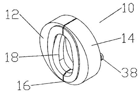
Figure 1 is a side schematic view of a split ring, according to an exemplary
embodiment of the invention, in an initial casting configuration.
3
i I I li .I ry iilil i .
Hd
CA 02584115 2007-04-03
Figure 2 is a schematic end view of a split ring, according to an exemplary
embodiment of the invention, in an initial casting configuration.
Figure 3 is a schematic isometric view of the split ring of figures 1 and 2,
folded
along the web portion and interconnected end to end.
Figure 4 is a schematic end view of figure 3.
Figure 5 is a schematic cross section view along line D-D of figure 4.
Figure 6 is a schematic close up view of area E of figure 5, showing an
exemplary retaining means in the form of an interference fit.
Figure 7 is a schematic isometric view of an overbody according to the
exemplary embodiment.
Figure 8 is a schematic interface end view of the overbody of figure 7.
Figure 9 is a schematic cross sectional view of the exemplary embodiment
installed upon a waveguide.
4
i I~ ,,
I I I I N d I
CA 02584115 2007-04-03
Figure 10 is a schematic close up view of area C of figure 9, showing an
exemplary retaining means in the form of an interference fit.
Figure 11 is a schematic isometric view of a waveguide seal according to the
exemplary embodiment.
Figure 12 is a schematic end view of the waveguide seal of figure 11.
Figure 13 is a schematic cross sectional view of a first alternative
embodiment
installed upon a waveguide.
Figure 14 is a schematic cross sectional view of a second alternative
embodiment installed upon a waveguide.
Figure 15 is a schematic close up view of area J of Figure 14.
Figure 16 is a side schematic view of a split ring, according to the second
alternative embodiment of the invention, in an initial casting configuration.
Figure 17 is a schematic close up view of area K of Figure 16.
Figure 18 is a schematic isometric view of the split ring of figure 16, folded
along
the web portion and interconnected end to end.
M 6
CA 02584115 2007-04-03
Figure 19 is a schematic interface end view of an overbody, according to the
second altemative embodiment of the invention.
DETAILED DESCRIPTION
As shown in figures 1-6, a split ring 10 according to an exemplary embodiment
of
the invention is formed as a single contiguous component. A first half 12 and
a
second half 14 of the split ring 10 are joined by a web portion 16. The web
portion 16 may be dimensioned with respect to the selected split ring 10
material.
For example, where a polymer is applied a thinner web portion 16 may be usable
according to elastic properties of the polymer, if any. Where a metal alloy is
applied, the web portion 16 preferably has a thickness that allows easy
folding of
the first and second halves 12, 14 toward one another without requiring
application of force multiplication means such as hand tools, and also that is
not
under or oversized such that the web portion 16 fractures upon folding.
An inner surface 18 of each of the first and second halves 12, 14 is formed to
match corrugations, if any, of the waveguide 20 exterior around which the
first
and second halves 12, 14 may be folded towards each other along the web
portion 16. Where a material with elastic rather than deformation retention
properties along the web portion 16 is applied, to retain the first and second
halves 12, 14 in a closed position around the waveguide 20, a retaining means
6
I 1 M AI
CA 02584115 2007-04-03
22 may be incorporated into the web portion 16 according to a deformation
retention characteristic of the selected material and or applied at the split
ring
end(s) 24. The retaining means 22 may be formed, for example, as a socket 26
of the second half 14 into which a pin 28 of the first half 12 makes an
interfeirence, annular or cantilever snap fit as the first and second halves
12, 14
are closed towards each other by folding along the web portion 16. Alternative
retaining means 20 include, for example, a tab into slot or fastener assisted
closure.
As shown in figures 7 and 8, an overbody 30 has a bore 32 dimensioned to
accept the expected waveguide cross section and an interface end 34 shoulder
36 formed in the bore 32 dimensioned to receive the split ring 10. One or more
alignment protrusions 38 formed in a waveguide side 40 of the split ring may
be
positioried to mate with corresponding alignment holes 42 formed in the
shoulder
36. As shown in figures 9 and 10, as the overbody 30 is pulled toward a split
ring
closed around the waveguide 20 exterior, the alignment protrusions 38 key into
the alignment holes in, for example, an interference fit, rotationally
aligning and
retaining the split ring 10 against the shoulder 36 of the overbody 30.
Alternatively, the keying between the alignment protrusions and alignment
holes
may be via annular or cantilever snap fit.
To environmentally seal the interior areas of the overbody 30, a waveguide
seal
44 as stiown in figures 10 and 11 may be applied between the overbody 30 and
7
i 11
LI N i qi q i .
I II IY dl
CA 02584115 2007-04-03
the split ring 10. Preferably, an interior surface 46 of the waveguide seal 44
has
features matching the waveguide 20 corrugations.
Once the waveguide 20 is mated with the overbody 30 via the split ring 20, any
desired interface element 48 may be securely fastened to the interface end 34,
for example via fasteners 50 such as bolts that fit through interface hole(s)
52 of
the overbody 30 interface end 34 and thread into the selected interface
element
48. An interface sealing groove or sealing shoulder 54 that together with the
periphery of the split ring 10 forms a groove may be applied to the interface
end
34 of the overbody 30 as a seat for a seal 56 such as an o-ring positioned
between the interface element 48 and the overbody 30.
To assemble the waveguide interface upon a waveguide, the waveguide 20 end
is passed though the overbody 30 bore 32 and the waveguide seal 44, if
present,
placed over the waveguide 20 end. The first and second halves 12, 14 of the
split ring 10 are folded along the web portion 16 to mate the split ring 10
with the
exterior of the waveguide 20. A retaining means 22 such as the pin 28 and
socket 26 are joined to retain the first and second halves 12, 14 around the
exterior of the waveguide 20. The overbody 30 is then drawn towards the split
ring 10 to compress the waveguide seal 44 and seat the split ring 10 within
the
interface end 34 shoulder 36. If present, alignment protrusions 38 of the
split ring
seat within alignment holes 42 of the interface end shoulder in an
interference
fit. If applicable, the interface end 34 of the waveguide30 is flared against
the
8
1 11 1 Irõ1,
I
CA 02584115 2007-04-03
interface end 34 of the split ring 10 and a desired interface element 48
fastened
to the interface end 34 of the overbody 30.
One skilled in the art will appreciate that the split ring 10 and overbody 30
may
be corifigured with no overhanging edges or threading as shown for example in
figures 1, 2, 7, 8 and 15-19. This enables application of precision injection
molding, die casting and or thixotropic metal molding technologies to cost
effectively form these components from polymers or metal alloys as desired.
Thereby, precision tolerances are achieved, eliminating the expense and
materials waste inherent with the prior precision metal machining production
steps.
In addition to materials cost savings, the use of polymers enabled by the
invention significantly reduces the weight of the resulting assembly.
A first alternative embodiment, as shown in figure 13, demonstrates that the
single piece, for example, die cast split ring 10 may apply conventional
fastener(s) 50 such as screws that thread into threaded hole(s) 57 formed in
the
shoulder 36 of overbody 30. Where the split ring 10 and web portion 16 are
formed from a material, such as a metal alloy, with deformation retention
properties, the web portion 16 once in the folded position, without more, may
be
sufficient to retain the first and second halves 12, 14 in a closed position
around
9
I I III I 11Vq I
I~. I Y !I
CA 02584115 2007-04-03
the waveguide 20 exterior before the overbody 30 is fitted, allowing further
retaining means 22 to be omitted.
A second alternative embodiment, as shown for example in figures 14 - 19,
demoristrates how the overall materials requirements and size of the wave
guide
interface may be minimized. The alignment and split ring 10 to overbody 30
shoulder 36 retention function is performed by an outer snap protrusion 58
located along the split ring 10 periphery that mates with a corresponding snap
groove 60 formed in the overbody 30 shoulder 36. To rotationally align the
split
ring 10 within the overbody 30, the periphery of the snap ring 10 and the
corresponding shoulder 36 of the overbody 30 are formed with a non-circular
cross section, locking rotational alignment of the snap ring 10 and overbody
30
upon insertion. Although the presence of the snap groove 60 complicates
molding of the overbody 30 and or introduces a additional machining
requirement, the materials savings and overall weight reduction of the
resulting
waveguide interface is significant.
The waveguide interface adapter is demonstrated in exemplary embodiments
herein with respect to a waveguide 20 having an elliptical cross section and
helical corrugations. One skilled in the art will appreciate that the
invention is
similarly applicable to a waveguide 20 having any desired cross section and
corrugations, if any, of any configuration.
i I II' r1qq '
u F
CA 02584115 2007-04-03
Table of Parts
split ring
12 first half
14 second half
16 web portion
18 inner surface
waveguide
22 retaining means
24 split ring end
26 socket
28 pin
overbody
32 bore
34 iriterface end
36 shoulder
38 alignment protrusion
waveguide side
42 alignment hole
44 waveguide seal
46 interior surface
48 interface element
fastener
52 interface hole
11
CA 02584115 2007-04-03
54 sealing shoulder
56 seal
57 threaded hole
58 outer snap protrusion
60 snap groove
Where in the foregoing description reference has been made to ratios,
integers,
components or modules having known equivalents then such equivalents are
herein incorporated as if individually set forth.
While the present invention has been illustrated by the description of the
embodiments thereof, and while the embodiments have been described in
considerable detail, it is not the intention of the applicant to restrict or
in any way
limit the scope of the appended claims to such detail. Additional advantages
and
modifications will readily appear to those skilled in the art. Therefore, the
invention in its broader aspects is not limited to the specific details,
representative apparatus, methods, and illustrative examples shown and
described. Accordingly, departures may be made from such details without
departure from the spirit or scope of applicant's general inventive concept.
Further, it is to be appreciated that improvements and/or modifications may be
made thereto without departing from the scope or spirit of the present
invention
as defined by the following claims.
12