Note: Descriptions are shown in the official language in which they were submitted.
CA 02584390 2012-03-29
Resettable Latching MEMS Shock Sensor Apparatus and Method
BACKGROUND
Field of the Invention
[0003] The present invention relates generally to a shock sensor and method
for
monitoring shock. More particularly, the present invention relates to a low-
power and
unpowered micro-electromechanical shock sensor using a micromechanical
suspended proof
mass structure.
Background of the Invention
[0004] Embedding miniature sensors in products, systems, storage and shipping
containers,
and other items allows the monitoring of those items to determine health,
maintenance needs,
lifetime, and other item characteristics. Information from miniature shock
sensors can tell
I
CA 02584390 2012-03-29
a user whether the item has been exposed to shock levels that can cause
damage. In addition,
miniature shock sensors can be used to "wake up," from a low-power sleep mode,
a more
sophisticated sensing system to collect a more complete set of environmental
data.
[00051 Current battery-powered embedded sensor systems that perform this type
of
monitoring often require a low power method of determining when a certain
level of shock has
been reached. Many other applications, such as in transportation and shipping
monitoring,
heating and air conditioning, and food storage, would benefit from the ability
to monitor the
shock environment with a completely unpowered sensor. In addition, these
applications would
benefit from the ability to poll that sensor to determine if a shock extreme
was reached, and then
reset the sensor for later use. In either case, an ultra-low power sensor, or
even a sensor that
consumes no quiescent power, would reduce the overall system power consumption
enough to
allow embedded sensors to operate for many years in portable battery powered
applications, or in
systems that scavenge small amounts of power from the environment.
100061 Low power and unpowered shock sensors currently exist. However, they
are
large-scale devices such as the catches used in automotive seat belts. These
devices operate in a
similar fashion and provide a similar function as the present invention, but
are not in a form
factor suitable for integration with microdevices, and are not fabricated
using techniques that are
compatible with microelectronics or micro-electromechanical systems ("MEMS")
devices.
[00071 Micro-scale shock sensors, in the form of accelerometers, exist as
well, but most
of the previous work to develop low-power shock sensors has been focused on
minimizing the
power consumption of standard miniature devices, and using low-power analog
electronics to
determine when a specific shock level has been reached. Devices and systems
would then create
2
CA 02584390 2012-03-29
a low-impedance logic level signal for input to a sleeping microcontroller.
The fundamental
problem is that such a system must continuously power the sensor and analog
trigger circuitry,
creating a constant power draw on the batteries. Even using the latest in low-
power devices and
highest capacity batteries, systems that continuously power any sensor will
only operate for 5 -
years.
[00081 As embedded miniature sensors get smaller, and as batteries are reduced
in size
and capacity, the use of lower power and unpowered devices will become more
critical.
Furthermore, maximizing the sensor functionality, without increasing power
consumption, will
enhance the capability of embedded sensing systems.
100091 Other inventions have used suspended proof mass micro-machined devices
to
measure shock, and for switching, but, until the present invention, only one
as had the
advantages of the present invention in combining low- or no-power operation
with a mechanical
latching function. U.S. Patent No. 6,737,979 discloses a MEMS shock sensor
that achieves the
goals of low- and no-power operation of a mechanical shock sensor with a
mechanical latching
function. In this prior art invention, as in the present invention, a moveable
proof mass and a
latching means are formed on the surface of a substrate. When the sensor is
subject to a
sufficient shock, the proof mass moves and latches with the latching means,
and the latched
condition is detected by external circuitry.
[00101 . The present invention offers several improvements to the technology
disclosed in
U.S. Patent No. 6,737,979 ("the `979 invention"). First, in the `979
invention, each separate
device design can detect only one range of shock level because the distance
between the proof
mass and the latch is not variable. In the present invention, the latching
distance is variable and a
3
CA 02584390 2012-03-29
sensor can therefore be programmed to detect varying shock levels. Second, in
the `979
invention, the only electrical contact made between the proof mass and the
latch to detect a
shock level is through the latch itself. As is discussed in detail below, the
present invention
offers a contact that is separate from the latch so that a "triggering"
condition (i.e., the proof
mass contacting with the contact) can be made (and detected) prior to
latching, if desired by the
user. With this feature, the present invention can be programmed to detect a
shock level smaller
than that of the latching shock level. Third, although the `979 invention
offers an unlatching
function so that the sensor can be re-used, the present invention improves
upon this function with
a mechanical linkage that applies no load to the latch during latching,
thereby decreasing the
necessary latching force and increasing the sensitivity of the sensor.
SUMMARY OF THE INVENTION
[0011] It is therefore an object of the present invention to provide a low-
power micro-
machined shock sensor in which the sensitivity of the sensor can be adjusted.
[0012] It is another object of the present invention to provide a low-power
micro-
machined shock sensor which allows for detection of a shock level separate
from and variable
from the latching function (i.e., a triggering event separate from a latching
event).
[0013] It is yet another object of the present invention to provide a
micromachined shock
sensor with an unlatching apparatus that does not apply a mechanical load on
the latch during
latching.
[0014] The present invention achieves these objectives with a micromachined
proof mass
connected to a substrate through micromachined flexures. The proof mass
includes a contact
area and a latching area. The contact area and latching area register
respectively with spring-
4
CA 02584390 2012-03-29
loaded contacts and a spring-loaded latch that are anchored to the substrate.
Under a shock load
of sufficient magnitude, the proof mass displaces to bring the contact area
together with the
spring-loaded contacts and to force the latch on the proof mass to engage with
the spring-loaded
latch. After latching, the contacts remain closed, allowing a voltage source
to be connected to the
input of a microcontroller, or allowing the completion of an external circuit.
A thermal,
capacitive, or other actuator can then be used to disengage the latch and
return the proof mass to
its original position. The sensor will use nearly zero power except when
actually providing the
trigger signal to the microcontroller or during any reset operation. The
sensor can remain latched
for interrogation at a later date, even if system power is lost, and the
sensor can be reset to detect
the next event.
10014a] In one particular embodiment there is provided a micro-
electromechanical shock
sensor device, comprising: a moveable proof mass comprising a first mechanical
latch and a first
electrical contact; and a pawl comprising a second mechanical latch, the
second mechanical latch
disposed at a latching distance from the first mechanical latch, the latching
distance
corresponding to a latching threshold shock level; and a second electrical
contact disposed at an
electrical contact distance from the first electrical contact, the electrical
contact distance
corresponding to an electrical contact threshold shock level; wherein the
first mechanical latch
moves toward the second mechanical latch and the first electrical contact
moves toward the
second electrical contact when the proof mass experiences a shock level in the
direction of the
latching threshold shock level; and wherein the first mechanical latch engages
with the second
mechanical latch when the shock level reaches the latching threshold shock
level; and wherein
the first electrical contact contacts with the second electrical contact when
the shock level
reaches the electrical contact threshold shock level.
[0014b] In another particular embodiment there is provided a method for
sensing shock
using a micro-electromechanical device, comprising the steps of: fabricating a
micro-
electromechanical shock sensor device, comprising: a moveable proof mass
comprising a first
mechanical latch and a first electrical contact; and a pawl comprising a
second mechanical latch,
CA 02584390 2012-03-29
the second mechanical latch disposed at a latching distance from the first
mechanical latch, the
latching distance corresponding to a latching threshold shock level; and a
second electrical
contact disposed at an electrical contact distance from the first electrical
contact, the electrical
contact distance corresponding to an electrical contact threshold shock level;
wherein the first
mechanical latch moves toward the second mechanical latch and the first
electrical contact
moves toward the second electrical contact when the proof mass experiences a
shock level in the
direction of the latching threshold shock level; and wherein the first
mechanical latch engages
with the second mechanical latch when the shock level reaches the latching
threshold shock
level; and wherein the first electrical contact contacts with the second
electrical contact when the
shock level reaches the electrical contact threshold shock level; and
installing the sensor in a
location in which shock is desired to be monitored.
[0015] For purposes of summarizing the invention, certain aspects, advantages,
and
novel features of the invention have been described herein. It is to be
understood that not
necessarily all such advantages may be achieved in accordance with any one
particular
embodiment of the invention. Thus, the invention may be embodied or carried
out in a manner
that achieves or optimizes one advantage or group of advantages as taught
herein without
necessarily achieving other advantages as may be taught or suggested herein.
[0016] These and other embodiments of the present invention will also become
readily
apparent to those skilled in the art from the following detailed description
of the embodiments
having reference to the attached figures.
DESCRIPTION OF THE DRAWINGS
[0017] Figure 1 is a schematic diagram of the shock sensor and its components.
6
CA 02584390 2007-04-17
WO 2006/127035 PCT/US2005/037675
[0018] Figure 2A is a high-level flowchart for an embodiment of a process
according to
the present invention.
[0019] Figures 2B -2F illustrate steps in the process of fabricating one
embodiment of the
present invention.
[0020] Figure 3 is a top view of the illustrated embodiment of the sensor in
its normal
state and ready to sense shock extremes.
[0021] Figure 4 is a diagram of the illustrated embodiment of the sensor in
its latched and
contacted state after a shock extreme has been reached.
[0022] Figure 5 shows the definition of parameters used in the design of the
sensor.
[0023] Figure 6 is a diagram of electrical interconnection of the sensor.
[0024] Figure 7 shows an embodiment of the invention with shock sensitive
contacts that
allow operation at lower shock levels.
[0025] Figure 8 shows an embodiment of the invention with multiple contacts
for
detection of multiple shock levels.
[0026] Repeat use of reference characters throughout the present specification
and
appended drawings is intended to represent the same or analogous features or
elements of the invention
DETAILED DESCRIPTION
[0027] The illustrated embodiment of the invention is fabricated in a thick
layer of
silicon or other conductor material that has been released from a rigid
substrate. Within this thick
7
CA 02584390 2007-04-17
WO 2006/127035 PCT/US2005/037675
layer of material, a proof mass, a set of flexures, multiple contacts,
multiple latch and pawl
structures, multiple actuators, and multiple anchors and pads are fabricated.
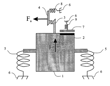
[00281 FIG. 1 illustrates a schematic diagram of one embodiment of the
invention. The
invention utilizes a micromachined proof mass structure 1 attached to the
substrate (not
illustrated) via anchors 6 through proof mass flexures 5. The proof mass
structure 1 includes a
contact area 2 and a latch 3. Under. a shock load, the inertia of the proof
mass yields a force, Fg,
that displaces the mass sufficiently to force the latch 3 to engage with a
similar latch on a thin
pawl 4 attached to the substrate via anchor 6 through pawl flexure 8. The
force also causes the
proof mass contact area 2 to connect with the contact 7 that is attached to
the substrate via anchor
6 through contact flexure 9. After latching, the contacts remain closed, and
the shock sensor can
then be interrogated by external circuitry (not illustrated). A thermal,
capacitive, or other
actuator (discussed below) can be used to develop a force, Fa, and disengage
the pawl 4 and
return the proof mass 1 to its original position.
[00291 FIG. 2A illustrates the high-level process flow for the process used to
fabricate
the suspended proof mass structure that is used in one embodiment of the
invention. While the
following discussion focuses on producing a silicon structure with the process
discussed herein,
other combinations of materials and other processes can be employed.
[00301 Employing the process of FIG. 2B and 2C, the starting material is a
silicon-on-
insulator ("SOI") wafer 26 with a handle layer 20 and a 100-micron thick
active silicon layer 22
separated by a 2 micron thick silicon dioxide layer 21. With attention to FIG.
2C, which
illustrates step 12 in greater detail, the SOI wafer 26 is first patterned
with photoresist 23 using
standard lithography to define the footprint of a suspended proof mass 24
(illustrated in FIG.
8
CA 02584390 2007-04-17
WO 2006/127035 PCT/US2005/037675
2D). As illustrated in FIG. 2D, which shows step 13 of the fabrication
process, a deep silicon
reactive ion etch defines the structure of the suspended proof mass 24.
[00311 As is illustrated in FIG. 2E (step 14), after the silicon pattern is
transferred, the
silicon dioxide layer 21 in between the silicon layers is removed with an
isotropic oxide etch that
allows portions of the layer 21, specifically those underneath anchors and
bond pads (not
illustrated), to remain and hold the structure to the substrate. After the
proof mass 24 and other
components are released from the substrate, the entire device is coated at an
angle with a metal
layer system using a process that places metal 25 on the sidewalls of the
structure, as illustrated
in FIG. 2F (step 15). This metal is critical as it forms the contacts that the
sensor uses.
[0032] FIG. 3 illustrates an embodiment of the invention that includes two
"mirror-
imaged" sets of latches/contacts on opposite sides of the proof mass 1 to
monitor both positive
and negative y-axis shock levels, and provides both a latch signal and a
programmable trigger
signal depending on the level of external ' shock. For example, the shock
level may not be
sufficient to cause the latches to engage (thus providing a "latch signal"),
but may be sufficient
for the contacts 2 and 7 to meet (this contact situation is discussed as a
"trigger signal" for the
purposes of this specification). The proof mass 1 responds to shock levels by
displacing itself in
the +y or -y direction. The latch 3 on the proof mass 1 is separated from the
pawl 4 by a
predetermined distance selected for the shock level at which the shock sensor
is desired to latch.
If that shock level is achieved, the proof mass 1 and latch 3 will move the
distance required to
engage the latch 3 with the pawl 4. A very flexible beam 50 allows the pawl 4
to move easily in
a direction perpendicular to the motion of the proof mass 1, and to engage
with the latch 3 which
prevents the proof mass 1 from returning to its initial state. At this point,
the shock sensor is in
its latched state and a closed contact exists between the proof mass 1 and
pawl 4. This closed
9
CA 02584390 2007-04-17
WO 2006/127035 PCT/US2005/037675
contact can function to signal a microcontroller or to allow interrogation by
an external reader.
FIG. 4 illustrates the shock sensor in a latched state.
[0033] In addition, as is shown in FIG. 3, when the proof mass 1 is deflected
by a shock,
the proof mass contact 2 on the sidewall of the latch 3 may connect with
contact 7. The surface
of the contact sidewalls (2 and 7) are designed to provide a reliable and low-
resistance contact.
The contact actuator 51 connected to the contact 7 allows the distance between
the contacts 2 and
7 to be varied. The contact actuator 51 achieves this by deflecting (upon the
application of a
current through external circuitry, not illustrated) in a direction generally
perpendicular to the
direction of the movement of the proof mass 1 (in the + or - x direction).
This ability-of the
sensor to vary the distance between the contacts 2 and 7 modifies the shock
level required to
make contact and thus provides user programmability. When the contacts 7
connect to the latch
contacts 2, a circuit can be closed that can provide a signal to a
microcontroller or be interrogated
by an external reader. The shock level for making a contact between the proof
mass contact 2
and the contact 7 may or may not be the same as that for latching depending on
the setting of the
contact actuator 51. In other embodiments of the invention, the latching shock
can be adjusted as
well by varying the distance between the latch 3 and the pawl 4 via adjustment
of the reset
actuator 53 in a manner similar to that of the contact actuator 51 discussed
above. Therefore, in
different embodiments and applications there could be instances in which the
contacts 2 and 7
make contact before latching occurs (via latch 3 and pawl 4). Conversely,
there could also be
instances in which latching occurs (via latch 3 and pawl 4) before the
contacts 2 and 7 make
contact.
[0034] The shock sensor is designed to be reset after the sensor (in its
latched state) is
read or used to provide a signal to an external system. As shown in FIG. 3,
the invention
CA 02584390 2007-04-17
WO 2006/127035 PCT/US2005/037675
includes a mechanical linkage 52 on the pawl 4 that creates a unique
mechanical connection to a
reset actuator 53. When the shock sensor is unlatched and ready to sense a
shock event, the reset
actuator 53 is not in contact with the mechanical linkage 52 or the pawl 4.
When a shock event
occurs, the latch 3 on the proof mass 1 makes contact with the pawl 4 and
forces the pawl 4 to
move in a direction generally perpendicular to the motion of the proof mass 1.
If the shock is of
sufficient magnitude, the latch 3 will push the pawl 4 until latching occurs.
The mechanical
linkage 52 is designed so that the reset actuator 53 does not apply a
mechanical load to the pawl
4 during latching. Without such a mechanical linkage 52, the reset actuator 53
would apply a
stiff resistance to the latching motion, making the sensing of low shock
levels difficult.
Although FIG. 3 illustrates one embodiment of such a mechanical linkage 52,
other mechanical
designs within the scope of the present invention would also achieve the goal
of permitting
latching to occur without resistance from the reset actuator 53.
[0035] While the sensor is in a latched state, as is shown in FIG. 4, the
reset actuator 53
can be forced to deflect such that the reset actuator 53 engages with the
mechanical linkage 52
and pulls the pawl 4 away from the latch 3. The illustrated embodiment of the
invention uses for
the reset actuator 53 a thermal actuator that deflects when a specific amount
of current is run
through the device. Once the actuator 53 is engaged with the pawl 4, the force
from the reset
actuator 53 will pull the pawl 4 away from the proof mass 1. When sufficient
force is applied, the
latch 3 and pawl 4 disengage, thereby releasing the proof mass 1 and allowing
it to return to its
initial position. At this point, the sensor is ready to monitor another shock
event.
[0036] FIG. 5 defines the primary parameters used to design one embodiment of
the
sensor to detect specific levels of shock. The mass of the proof mass defines
the inertial force,
and is given by the following expression:
11
CA 02584390 2007-04-17
WO 2006/127035 PCT/US2005/037675
m=p*wm*lm*t
where m is the mass, p is the density of the material, wm is the proof mass
width, lm is the proof
mass length, and t is the thickness of the proof mass.
[0037] The inertial force developed on the mass under acceleration is then
given by:
F=m*a
where F is the inertial force, m is the mass of the proof mass, and a is the
applied acceleration..
[0038] The stiffness of the suspension provides a force against the inertial
force. The
stiffness is given by:
k=2*kb= 2*E*t*wb3
lb3
where k is the entire suspension stiffness, kb is the stiffness of one beam in
the suspension, E is
the Young's modulus of the material the device is made in, wb is the width of
a beam in the.
suspension, lb is the length of a beam in the suspension, and t is the
thickness of the material.
[0039] The distance the proof mass will move under the applied acceleration,
neglecting
the effects of the latch friction, is given by:
F
Y _ k
A device will latch if the proof mass deflection is greater than the distance
of the latch gap plus
the distance across the tip of the pawl, and can be expressed by the following
latching condition:
12
CA 02584390 2007-04-17
WO 2006/127035 PCT/US2005/037675
a > k * (lg+ lp)
M
[0001 Table 1 below contains the shock levels required for latching the sensor
given a
set of design parameters and a material thickness of 100 m and a latching gap
of 7 m.
Shock Flexure Width, Flexure Length, Proof Mass Proof Mass
Level wb lb Width, wm Length, lm
20g 3.5 m 800 m 1500 m 1100 m
250g 5 m 800 m 515 m 515 m
500g 6.5 m 800 m 545 m 545 m
1000g 8.5 m 800 m 581 m 581 m
Table 1 - Table of design parameters versus shock trigger levels
[0040] In one embodiment of the invention, the shock sensor is used to wake up
a
microcontroller in an embedded sensing application. In other embodiments, the
device is used in
standalone applications where the sensor is connected to an RFID tag or other
transmitter for
remote determination of the shock environment experienced by shipping
containers and
products. Similar devices for other environmental variables such as
temperature, humidity, and
chemical concentrations can be developed using the principles disclosed
herein.
[00411 FIG. 6 illustrates a wiring schematic for an embodiment of the
invention that is
used for waking up an embedded microcontroller from a sleep mode when a
certain shock level
is experienced. In this embodiment, a voltage difference is applied across
actuators 53 and 51.
In operation a single bias signal is applied to the proof mass 1 of the
device. The bias signal
could be a voltage or current depending upon the type of readout circuit used.
Connections to
the external contacts and pawls would be outputs to which the bias signal is
connected. These
13
CA 02584390 2007-04-17
WO 2006/127035 PCT/US2005/037675
outputs could be connected to microcontroller interrupt lines, to a wireless
transceiver, to a large
circuit network that performs some function, or a number of other connection
and circuits.
[0042] Although several embodiments and forms of this invention have been
illustrated,
it is apparent that those skilled in the art can make other various
modifications and embodiments
of the invention without departing from the scope and spirit of the present
invention. For
example, other configurations of the sensor are possible that utilize varying
surface features on
the contacts, multiple movable contacts, and different actuator types.
[0043] One particular embodiment of the invention, shown in FIG. 7, uses the
sidewall
40 of a second proof mass 41 as a moving contact to connect with the contact
42 on the sensor's
main latching proof mass 1. When a shock load is applied, the moving contact
41 will move out
of the way of the main proof mass 1 during the latching operation, thereby
reducing the amount
of force required to meet the latching condition. After the latching occurs
and the shock load is
removed from the device, the moving contact 41 will return to its original
position and make a
connection with the contact 42 on the device's main latching proof mass 1.
This configuration is
useful when designing low shock trigger devices where the inertial force may
be insufficient to
overcome the retarding force created by the stationary electrical contacts.
[0044] Another embodiment, shown in FIG. 8, includes multiple contacts 70 and
multiple latches 71 to allow one sensor device to trigger at and latch at
multiple shock levels that
the proof mass 1 is subjected to.
[0045] Another embodiment of the device (not illustrated) uses a capacitive
actuator for
reset functions instead of a thermal actuator. A capacitive actuator consumes
less power but
would be suitable only for lower force and lower shock level applications. The
configuration
14
CA 02584390 2012-03-29
would require additional capacitive actuators on the proof mass to move it out
of contact with
the pawl, thereby eliminating the friction that holds the pawl in contact with
the latch. Only then
could another capacitive actuator move the pawl out of position, after which
the actuator on the
proof mass is released, followed by the release of the pawl, at which point
the sensor is
unlatched and ready for another sensing operation.
100461 Furthermore, other fabrication processes for the device are possible.
Any
fabrication process that realizes a single thick micromechanical structural
layer with 1)
conducting sidewalls that can make electrical contact, and 2) large amounts of
suspended inertial
mass. Examples include bulk micromachining and wafer-bonding fabrication
approaches in
silicon, silicon dioxide, nickel, titanium and other conductors, as well as
LIGA-type fabrication
processes using electroplated metals.
[0047[ As described above and shown in the associated drawings, the present
invention
comprises a micro-electromechanical shock sensor. While particular embodiments
of the
invention have been described, it will be understood, however, that the scope
of the claims should
not be limited by the preferred embodiments set forth above. The claims should
be given the
broadest interpretation consistent with the description as a whole.