Note: Descriptions are shown in the official language in which they were submitted.
CA 02584564 2007-04-18
WO 2006/044887 PCT/US2005/037422
OPTICAL DETECTOR CONFIGURATION AND UTILIZATION AS
FEEDBACK CONTROL IN MONOLITHIC INTEGRATED OPTIC AND
ELECTRONIC ARRANGEMENTS
Cross-Reference to Related Application
This application claims the benefit of US Provisional Application No.
60/620,156, filed October 19, 2004.
Technical Field
The present invention relates to the fabrication of monolithic arrangements of
integrated optic and electronic devices and, more particularly, to the
utilization of optical
detector feedback configurations to provide closed-loop control of such
monolithic
arrangements.
Background of the Invention
In an SOI-based opto-electronic platfonn, relatively thin (e.g., <1 m)
silicon
waveguides are used to distribute light across the entire chip and provide
multiple optical
functions (for example, splitting/combining, modulation, switching, wavelength
multiplexing/demultiplexing, add/drop, equalization and dispersion
compensation). The
ability for light coupling and manipulation in a thin waveguide on an SOI
platform
enables a true integration of optics and microelectronics on a siiigle silicon
chip. One of
the reasons for the high cost, high power consumption and large form factors
of the
optical components/subsystems in the optical communication industry is the
lack of
available component integration. Today's opto-electronic industry relies on
discrete
building blocks and hybrid integration of various components inade out of
various
material systems. Similar to the IC industry in the 1960s, these discrete
components are
open loop, where the loop is then closed externally (using, for example,
external optics
and electronics), resulting in lower yields and high costs.
To realize the full potential of the monolithic integration of optics and
electronics
on silicon, the performance and yield of the optical and opto-electronic
functions must be
improved to match the performance and yield of the electronics. Thus, a need
remains in
the art for an on-chip solution for managing variations in the optical
performance and
improve the overall operability of such devices.
1
CA 02584564 2007-04-18
WO 2006/044887 PCT/US2005/037422
Summary of the Invention
The need remaining in the prior art is addressed by the present invention,
which
relates to the fabrication of monolithic arrangements of integrated optic and
electronic
devices and, more particularly, to the utilization of optical detector
feedback
configurations to provide closed-loop control of such monolithic arrangements.
In accordance with the present invention, electronic feedback control
circuitry is
formed as a monolithic arrangement within the surface silicon layer of a
silicon-on-
insulator (SOI) structure, along with the desired electronic and optic
devices, allowing
for optimization of optical performance in the presence of situations such as
manufacturing variations, temperature fluctuations, power supply variations,
aging, etc.
The feedback loop is closed by the use of an optical detector is association
with the
feedback electronics.
The monolithic feedback electronics includes, at least, an A/D converter for
transforming an analog output from the associated photodetector into a digital
representation. Control electronics, responsive to the output from the A/D
converter, is
used to supply a feedback signal to one or more components of the opto-
electronic
system in order to control the response of the system. In some embodiments of
the
present invention, an additional calibration and/or look-up table may be
included within
the monolithic feedback electronics and queried by the control electronics to
determine
the proper feedback signal. In further embodiments of the present invention,
there may
be a communication interface between the control electronics and an "off chip"
system
that is used to either initialize the control electronics, retrieve
performance data from the
control electronics, or both.
Various embodiments of the present invention utilize the inventive combination
of the monolithic feedback loop and optical detector to optimize, for example,
one or
more of the following: (1) the output power from an opto-electronic modulator;
(2)
optical input coupling power; (3) attenuation in a variable optical
attenuator; (4) filtering;
(5) arrays of optical devices and more.
Other and further embodiments of the present invention will become apparent
during the course of the following discussion and by reference to the
accompanying
drawings.
2
CA 02584564 2007-04-18
WO 2006/044887 PCT/US2005/037422
Brief Description of the Drawings
Referring now to the drawings,
FIG. 1 illustrates, in simplified form, an exemplary closed-loop feedback-
controlled SOI-based input coupling arrangement;
FIG. 2 contains a diagram of an alternative embodiment of the present
invention
that utilizes the monolithic feedback arrangement in association with a
modulator (in this
case, a Mach-Zehnder modulator);
FIG. 3 illustrates the utilization of the closed-loop inventive feedback
arrangement in conjunction with a variable optical attenuator (VOA);
FIG. 4 contains an exemplary embodiment of an optical filtering arrangement
utilizing the monolithic feedback electronics of the present invention;
FIG. 5 is an embodiment of the present invention particularly configured for
use
with a plurality of separate optical devices;
FIG. 6 contains a diagram of an exemplary optical switch utilizing the
monolithic
feedback arrangement of the present invention;
FIG. 7 illustrates an exemplary ring filtering arrangement using the feedback
arrangement of the present invention to control/modify the wavelength(s)
supported by
the ring;
FIG. 8 illustrates a variation of the embodiment of FIG. 7, where an in-line
optical detector is used in association with the feedback arrangement;
FIG. 9 illustrates another variation of the embodiment of FIG. 7, where in
this
case, a ring waveguide is used to block a signal from further propagation; and
FIG. 10 contains a diagram of an exemplary optical output coupling structure
as
controlled by the inventive feedback arrangement of the present invention.
Detailed Description
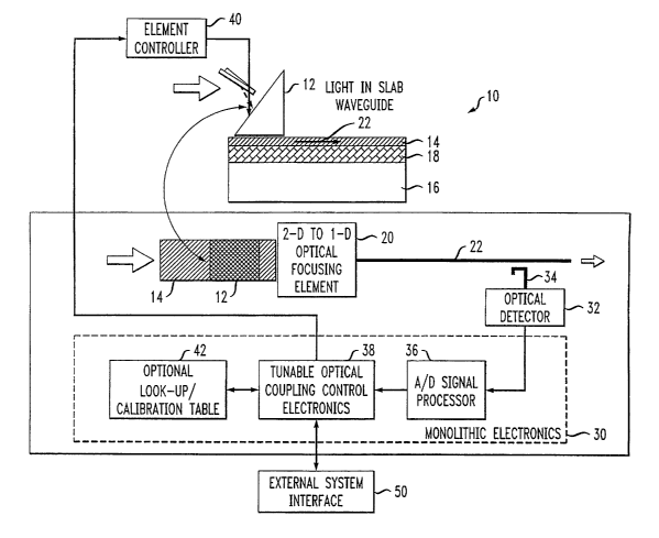
FIG. 1 illustrates, in a combination of a simplified top view and side view,
an
exemplary closed-loop feedback-controlled optical input coupling arrangement
10
formed in accordance with the present invention. As described in various other
prior
references regarding silicon-on-insulator (SOI) optical systems, a silicon
prism, such as
prism 12, is used to couple an optical signal into a sub-micron thick silicon
surface layer
14 of an SOI structure that further comprises a silicon substrate 16 and
buried oxide layer
18.
3
CA 02584564 2007-04-18
WO 2006/044887 PCT/US2005/037422
As shown particularly in to top view of FIG. 1, the coupled optical signal
passes
through a focusing element 20 and thereafter into a relatively thin optical
waveguide 22.
Focusing element 20, a silicon-based optical element, is used to convert the
two-
dimensional propagating optical signal into a one-dimensional optical signal,
bounded in
both its width and height by waveguide 22. It is well known that the
efficiency of this
type of coupling arrangement is based, at least in part, on the angle at which
the
incoming optical beam impinges input coupling facet 24 of prism coupler 12. In
the
particular arrangement as shown in FIG. 1, a movable reflective element 26
(such as, for
example, a MEMS device) is used to intercept the incoming light beam and
control the
orientation and/or position of the beam impinging input coupling facet 24.
In accordance with the present invention, a closed-loop, monolithic feedback
electronic arrangement 30 is used to measure the power of the optical signal
propagatirig
along waveguide 22, the coupled optical power being dependent in part upon the
amount
of light coupled in through prism 12. Advantageously, feedback electronics 30
may
comprise a monolithic structure of conventional electronic components used to
perform
well-known functions, as described below. As shown in FIG. 1, closed-loop
feedback
electronics 30 is coupled to the output of an optical detector 32 (such as,
for example, a
polygermanium, SiGe, silicide-based Schottky diode, etc) to capture a portion
of the
propagating output signal, using an optical coupler 34 to tap off a slight
portion (for
example, about 1%) of the signal propagating along waveguide 22. In this and
the
remaining figures, a thicker and darker lead line is used to illustrate an
"optical"
waveguide, with a thinner and lighter lead line used to illustrate an
"electrical" signal
path. It is to be understood that while feedback electronics 30 is illustrated
as integrated
within the same silicon substrate as the remainder of the opto-electronics
configuration,
feedback electronics 30 may also be formed on a separate substrate that is
thereafter
mated with the SOI-based opto-electronic structure. That is, a flip-chip or
stacked
integrated circuit arrangement may be used to provide the desired feedback
arrangement
of the present invention.
Referring back to FIG. 1, the analog electrical signal output from optical
detector
32 is thereafter applied as an input to an analog-to-digital (A/D) converter
36 within
monolithic feedback electronics 30, which functions to generate a digital
representation
of the measured optical signal. The digital representation is applied as an
input to a
tunable control electronics 38, which is programmed to analyze the signal, and
determine
4
CA 02584564 2007-04-18
WO 2006/044887 PCT/US2005/037422
if an adjustment in the input coupling orientation is required to improve the
input optical
coupling efficiency.
The output from tunable control electronics 38 is then used as a "control"
signal
electronic output from monolithic feedback electronics 30 to modify the input
coupling
arrangement, in this case as an input to a position adjustment arrangement 40
to alter the
position of optical element 26 and thus provide an adjustment in the input
coupling angle
and/or position of the optical signal at prism coupling facet 24. Optical
element 26 may
comprise, for example, a reflective element, a transmissive element or a train
of such
elements. In accordance with the present invention, optical detector 32 and
the various
electronic components within closed-loop monolithic feedback electronics 30
are
integrated within the same SOI structure as the remainder of the components in
the opto-
electronic arrangement. Thus, the monolithic closed-loop arrangement of the
present
invention is capable of continuously monitoring the performance of the
exemplary input
coupler and modifying the orientation of reflective coupling element 26, as
needed, as
the operating conditions change (e.g., ambient temperature, age of components,
etc.).
Although the particular embodiment illustrated in FIG. 1 utilizes a prism
device as an
input coupler, feedback electronics 30 may be used with a variety of other
coupling
arrangements (necessarily formed as active devices), including (but not
limited to),
inverse tapered waveguides, optical gratings, horn waveguides, where feedback
electronics 30 is utilized to "tune" the properties of such devices to achieve
maximum
coupling efficiency.
Advantageously, the utilization of a monolithic structure in accordance with
the
present invention allows for additional elements to be easily incorporated
within
inventive closed-loop feedback electronics 30. Referring to FIG. 1, a look-
up/calibration
table 42 may be added to feedback electronics 30, where in this particular
application
table 42 stores various optical power values, and a listing of input signal
wavelengths
and reflective element orientations associated with the power values.
Additionally, an
external system interface 50, located "off-chip" may be used to load initial
values into
controller 38 (such as during factory installation), or system interface 50
may be used to
interrogate controller 38 and download its stored values to external
monitoring systems
(as used, for example, for quality control/assurance purposes).
FIG. 2 illustrates an arrangement for utilizing closed-loop feedback
arrangement
30 of the present invention in association with a modulator 60, such as a Mach-
Zehnder
modulator. As shown in FIG. 2, modulator 60 includes an input waveguiding
section 62,
5
CA 02584564 2007-04-18
WO 2006/044887 PCT/US2005/037422
a Y-splitter 64 and a pair of parallel waveguides 66-1 and 66-2, where the
parallel
waveguides are thereafter re-coupled within a Y-combiner 67 into an output
waveguide
section 68. An optical input signal is coupled into input section 62, passes
through
parallel waveguides 66-1 and 66-2, and exits through output waveguide section
68. A
pair of phase shifting electrodes 70-1 and 70-2 are used to control the
optical path length
"seen" by signals propagating along waveguides 66-1 and 66-2, respectively, so
as to
adjust the characteristics of the output signal propagating along waveguide
section 68.
In accordance with the present invention, a portion of the optical output
signal
propagating along waveguide section 68 is tapped off by first waveguide
coupler 34-1
and applied as an input to a first optical detector 32-1. Similarly, a portion
of the applied
input signal propagating along input waveguide section 62 is tapped off by a
second
waveguide coupler 34-2 and applied as an input to a second optical detector 32-
2. It is to
be understood that as an alternative to utilizing an optical detector and
associated tap
waveguide, an "in-line" detector may be used, avoiding the need for an
additional
waveguide structure. As with the arrangement described above, the tapped-off
optical
signals are converted into analog equivalent representations. The pair of
analog signals
representing the optical input signal and the optical output signal are then
applied, as
separate inputs to monolithic feedback electronics 30 and, in particular, as
separate
inputs to A/D converter 36 (or, alternatively, each signal may be applied as
an analog
input to separate A/D converters).
The digital outputs from A/D converter 36 are thereafter applied as inputs to
control electronics 38, where in this application control electronics 38
performs an
analysis based, for example, upon the ratio of the measured signals. The
results of this
analysis is then used to determine if any modifications need to be made to the
signals
used to control modulator 60 (i.e., the signals applied to phase shifting
electrodes 70-1
and 70-2) so as to improve the performance of modulator 60. Properties such
as, for
example, extinction ratio, optical output power, optical "eye" quality and bit
error ratio
(BER) may all be analyzed by control electronics 38 of the present invention.
In
particular, acceptable values for each of these parameters may be stored
within controller
38 or, alternatively, in look-up table 42 (if such a table is present within
feedback
arrangement 30). By detecting the ratio of the power between the two
detectors, and
knowing the DC and AC voltages applied to each phase shifter, feedback
electronics 30
of the present invention can adjust one or both of the phase sifting
electrical input signals
to optimize the performance of modulator 60.
6
CA 02584564 2007-04-18
WO 2006/044887 PCT/US2005/037422
More generally, closed-loop feedback system 30 of the present invention may be
used in conjunction with modulator 60 to perform phase shifting through a
variety of
different methods, including introducing thermal changes to the phase shifting
elements
and/or by modifying free carrier charges within the waveguide. Dither tones,
as well
known in the art, may also be impressed upon the propagating signals and used
to
optimize the extinction ratio of modulator 60. In the particular utilization
of feedback
system 30 with modulator 60, look-up table 42 may be used to provide
temperature
compensation values.
Variable optical attenuators (VOAs) are utilized widely throughout optical
communication networks, primarily to control the optical power propagating
along a
waveguide. FIG. 3 illustrates the utilization of closed-loop monolithic
feedback
arrangement 30 in conjunction with an exemplary VOA 80 to accurately set and
control
the degree of attenuation that is provided. Referring to FIG. 3, VOA 80 is
illustrated as
disposed along an optical waveguide 82, with an input optical signal applied
along an
input waveguide section 82-I, which is thereafter coupled to the input of VOA
80. The
output from VOA 80 is then coupled into output waveguide section 82-0. In the
utilization of closed-loop monolithic feedback electronics 30 with VOA 80, a
first optical
detector 32-1 is used to measure the power level of the optical input signal
and a second
optical detector 32-2 is used to measure the power level of the optical output
signal, thus
providing a direct measure of the function of VOA 80.
As shown, the analog electrical representations of the measured input and
output
signals are applied as separate inputs to A/D signal processor 36 of feedback
electronics
30, where the digital outputs from processor 36 are thereafter applied as
inputs to control
electronics 38. As a function of the values for the digital representations,
control
electronics 38 will determine if any adjustments in the degree of attenuation
provided by
VOA 80 are required. A control signal output from electronics 38 is thus used
as an
adjusting input signal to VOA 80. As with the arrangements discussed above, a
calibration/look-up table 42 may be included within the monolithic feedback
electronics
30, where table 42 may store the various adjustment values required for
different
possible attenuation outputs. Also, control electronics 38 may include a
communication
path to external system interface 50, where this interface may be used to
initialize the
operation of control electronics 38, load values into table 42, communicate
new
attenuation settings to optimize the overall system performance, or serve as a
conduit to
download values stored in control electronics 38 for analysis by an off-chip
system.
7
CA 02584564 2007-04-18
WO 2006/044887 PCT/US2005/037422
Accordingly, as the operation of VOA 80 changes (as a function of, for
example,
changes in the ambient temperature or age of the devices), the change will be
measured
within closed-loop feedback system 30 and used to generate an electrical
feedback signal
that is applied as a control input to VOA 80 and modify the applied
attenuation, as need
be.
There are many optical communication systems that utilize filtering to provide
wavelength sensitivity to the system. Such filtering may be used to remove
"noise"
signals from a single wavelength signal propagating along a waveguide.
Alternatively,
an optical filter may be used to select one particular wavelength (or a group
of
wavelengths) for use from a number of different wavelengths presented as an
input. As
with the VOA arrangement discussed above, closed-loop monolithic feedback
electronics 30 of the present invention may be used in conjunction with an
associated
SOI-based optical filter to optimize its performance in light of variations
that may occur
over time (i.e., aging, temperature drift, etc.) or as a result of variations
in the
manufacturing/fabrication process, as particularly associated with integrating
optical
elements within an SOI-based structure.
FIG. 4 illustrates an exemplary SOI-based arrangement of an optical filter 90
disposed along an optical waveguide 92 (with an input waveguide section 92-1
and an
output waveguide section 92-2) and feedback electronics 30, all formed as a
monolithic
structure within the same SOI-based substrate. Particularly for situations
utilizing dense
wavelength division multiplexing (DWDM), where various input wavelength
signals are
closely spaced, the use of on-chip feedback in accordance with the present
invention
provides a highly reliable arrangement for accurately controlling the
wavelength of the
optical signal exiting optical filter 90. For example, as shown in FIG. 4, a
plurality of
optical signals operating at different wavelengths /%1, X2, ..., XN are
applied as inputs to
optical filter 90, where it is desired that only the signal operating at
wavelength XI be
further propagated. By measuring the value of this output signal with detector
32-2 of
feedback arrangement 30, the parameters of optical filter 90 can be adjusted
as necessary
to prevent drifting of the wavelength value.
As a further advantage of the monolithic arrangement of the present invention,
the closed-loop feedback may be used with an array of optical/opto-electronic
devices
formed on a single SOI substrate. FIG. 5 illustrates an exemplary embodiment
of the
present invention where closed-loop feedback electronics 30 is configured for
use with
8
CA 02584564 2007-04-18
WO 2006/044887 PCT/US2005/037422
an array of N optical devices 1001 - 100N, where the N devices may comprise a
variety of
different devices, or an array of identical devices. In this particular
embodiment of the
present invention, closed-loop feedback arrangement 30 further comprises a
pair of 1-of-
N electronic selectors 44-1 and 44-2, where selector 44-1 is coupled to
receive the
measured optical input signals from a plurality of optical detectors 32-11
through 32-1N
located at the input to the associated plurality of N optical devices 1001 -
100N.
Similarly, selector 44-2 is used to determine which one of the associated
optical output
signals from devices 1001 - I OON is to be analyzed at a particular time. As
shown,
selector 44-2 is coupled between the output of a plurality of optical output
detectors 32-
21 through 32-2N and the input of A/D converter(s) 36, such that the analog
output signal
from only a selected detector 32-2 will be applied as an input to A/D
converter(s) 36.
A monolithic, SOI-based optical switch arrangement 120, including feedback
electronics 30 of the present invention is illustrated in FIG. 6. As shown,
switch 120
included an input coupling element 122, such as a pair of evanescently coupled
waveguides, for introducing the input optical signal to the system. The signal
is then
split along waveguides 124-1 and 124-2, where a pair of phase shifters 126-1
and 126-2
are disposed along waveguides 124-1 and 124-2, respectively. By controlling
electrical
signals applied to phase shifters 126-1 and 126-2, the output optical signal
may be
configured to switch between a first output waveguide 128-1 and a second
output
waveguide 128-2. Various parameters associated with the optical switching
function
(such as, for example, its bit error rate (BER)) may be controlled, in
accordance with the
present invention by monitoring both the power present in the input optical
signal and
the optical signal power present along each output signal path.
In accordance with the present invention, therefore, a pair of output optical
detectors, denoted 32-outl and 32-out2 are disposed to tap off a portion of
the signal
propagating along waveguides 128-1 and 128-2, respectively. An input monitor
comprises an optical detector 32-in and associated waveguide 34-in. As with
the
arrangements described above, optical detectors 32-outl and 32-out2 generate
electrical
analog output signals, which are thereafter applied as inputs to A/D processor
36 of
monolithic electronics 30. The digital output from processor 36 is thereafter
applied as a
input to control electronics 38, which produces two output control signals,
denoted C-1
and C-2.
FIG. 7 illustrates an exemplary SOI-based wavelength selective arrangement (a
ring resonator structure in this case) that may use feedback electronics 30 of
the present
9
CA 02584564 2007-04-18
WO 2006/044887 PCT/US2005/037422
invention to provide the desired degree of wavelength tuning and control. An
exemplary
waveguide 140 is shown in FIG. 7, where a ring-shaped waveguide 142 is also
integrated
within the same SOI layer of the SOI-based structure as waveguide 140, and
disposed in
relationship with waveguide 140 so as to out-couple light propagating at a
particular,
selected wavelength. As is well-known in the art, the size and shape of a ring
waveguide
can be configured to as to allow for a particular wavelength of light to be
coupled out of
the waveguide and into the ring (alternatively, a particular wavelength of
signal injected
into ring waveguide 142 may be thereafter coupled into waveguide 140). In the
embodiment of FIG. 7, ring waveguide 142 is configured to out-couple light
propagating
at a selected wavelength %1 from the various set of wavelengths propagating
along
waveguide 140. Ring 142 may be "tuned" by virtue of a phase-shifting element
144
disposed, as shown, over a portion of ring 142. Phase-shifting element 144 may
comprise, for example, a thermal or free-carrier based type of device. The
application of
an electrical signal to phase-shifting element 144 functions to alter the
optical path length
of ring 142 as "seen" by a propagating signal, thus altering the wavelength
that will be
coupled into ring 142. Although only a single ring 142 is shown in FIG. 7, it
is to be
understood that a plurality of rings may be disposed along waveguide 140, with
each ring
"tuned" to out-couple a different wavelength, so as to perform
multiplexing/demultiplexing operations.
As shown in FIG. 7, a separate optical waveguide 146 is disposed adjacent to
ring
142 to capture the signal propagating at wavelength 2,1 and allow the signal
to continue
to propagate through the SOI layer of the arrangement. In accordance with the
present
invention, a first optical detector 32-1 and associated tap-off waveguide 34-1
are
disposed adjacent to waveguide 146 so as to remove a portion of the selected
signal for
analysis. A separate optical detector 32-2 and tap-off waveguide 34-2 are used
to
measure the signal remaining along the output of waveguide 140. Both of these
measured signals are thereafter applied as inputs to feedback electronics 30,
as shown.
In particular, the pair of measured signals are first digitized within A/D
signal processor
36 and then applied as digital inputs to control electronics 38. Control
electronics 38
performs an analysis on the characteristics of the selected wavelength versus
the
remaining un-selected wavelengths (signal power, "drift" of wavelength, etc.)
and based
on this information, generates an electronic control signal that is applied as
the feedback
to phase-shifting element 144. The applied control signal thus is used to
adjust the
CA 02584564 2007-04-18
WO 2006/044887 PCT/US2005/037422
characteristics of ring 142, as necessary, to ensure that the proper
wavelength(s) is out-
coupled from waveguide 140. As with the various embodiments described above, a
separate look-up table 42 and/or external system interface 50 may be used as
part of
feedback electronics 30.
FIG. 8 illustrates a slight variation of the embodiment of the FIG. 7, where
in this
case, an in-line photodetecting device 32-I is disposed along waveguide 146,
as shown.
In particular, in-line photodetecting device 32-I may comprise a traveling
waveguide
detector structure that is integrated within waveguide 146. As with all of the
other
embodiments, the analog electrical output signal from photodetecting device 32-
I is
applied as the input to A/D signal processor 36 of feedback electronics 30.
Another
alternative to the arrangement of FIG. 7 is illustrated in FIG. 9, where in
this particular
case the out-coupled wavelength is simply "blocked" from further propagation.
Therefore, for this embodiment, tap-off waveguide 34 associated with optical
detecting
device 32 is positioned adjacent to ring waveguide 142, so as to out-couple at
least a
portion of the particular wavelength that was removed from waveguide 140 by
the action
of ring 142. In the same manner as the embodiments of FIGs. 7 and 8, the
measured
signal as applied as an input to control electronics 38 may then be used to
adjust the
performance of ring 142 through the application of an electronic control
signal to phase-
shifting element 144.
As mentioned above, proper coupling orientation at the input of an SOI-based
structure is critical in achieving the desired degree of optical efficiency.
Equally
important is the output coupling arrangement utilized with SOI-based
structures. FIG.
10 illustrates an exemplary embodiment of the present invention where
monolithic
feedback electronics 30 is utilized in association with an off-chip element to
control the
tuning, alignment and focusing qualities of an optical signal as it is coupled
out of the
SOI-based structure. In this case, the output coupling optics comprises a pair
of
collimating elements (for example, two-dimensional lenses) 150 are used within
the
surface of the SOI substrate to convert the one-dimensional signals
propagating along
waveguides 152 into a two-dimensional, collimated form. An out-coupling device
154,
such as an optical prism, is then used to re-direct the two-dimensional signal
out of the
plane of the SOI substrate and into free space (where it is to be understood
that various
other types of coupling arrangements, such as tapers and/or gratings may be
used for
coupling). Tunable coupling element 156, as shown, is then used to properly
direct this
11
CA 02584564 2007-04-18
WO 2006/044887 PCT/US2005/037422
free space signal into associated guiding devices (such as optical fibers, or
waveguides
within a following structure).
Referring to FIG. 10, optical detector 32 is used to measure the ainount of
reflected signal present within an output coupling arrangement (where, of
course, in the
ideal arrangement the reflected signal would have a zero power value). By
measuring
the amount of reflected power, as translated into a digital signal by A/D
processor 36,
control electronics 38 may be used to adjust the orientation of off-chip
tunable coupling
element 156 so as to focus the free space propagating beam(s) into an
associated optical
fiber or other guiding element.
The foregoing description of specific embodiments of the present invention
have
been presented for purposes of illustration and description. They are not
intended to be
exhaustive or to limit the invention to the precise forms disclosed, and
obviously many
modifications and variations are possible in light of the above teaching. For
example,
while prism coupling is mentioned as the coupling technique for various
embodiments,
any suitable type of optical coupling for use with SOI-based structures may be
employed
and find benefit by virtue of incorporating the feedback arrangement of the
present
invention. Moreover, the feedback electronics may include one or more
components that
are supported on a separate substrate that is thereafter coupled to the SOI
substrate
supporting the opto-electronic elements (e.g., "flip-chip" bonded, stacking
arrangement
of substrates, etc.). Further, various types of photodetectors (discrete
devices or
integrated devices, waveguide-coupled or in-line) may be used to provide the
input
signal to the feedback electronics of the present invention. The embodiments
selected
for illustration were chosen and described in order to best explain the
principles of the
invention and its practical application, to thereby enable others skilled in
the art to best
utilize the invention and various embodiments, with various modifications as
are suited
to the particular use contemplated. It is intended that the scope of the
invention be
defined only by the claims appended hereto and their equivalents.
12