Note: Descriptions are shown in the official language in which they were submitted.
CA 02585625 2007-04-27
WO 2006/050337 PCT/US2005/039415
HIGH PERFORMANCE FINGERPRINT IMAGING SYSTEM
TECHNICAL FIELD
This invention relates to imaging devices for use, for example, with
fingerprint
imaging systems.
BACKGROUND
Up-to-date fingerprint imaging systems using fingerprint image transfer into
electronic data usually apply the known contact method to create a fingerprint
pattern.
A surface topography of a finger is approximated by a series of ridges with
intelinediate valleys. When a finger is applied to a surface of a transparent
optical
plate or prism, the ridges contact the optical plate while the valleys do not
and instead
serve to form the boundaries of regions of air and/or moisture.
The finger to be imaged is illuminated by a light source located below or near
the optical plate. Imaging light from the light source is incident on the
surface of the
optical plate at an angle of incidence measured with respect to a normal to
that
surface. Imaging light reflected from the surface is detected by an imaging
system
that includes some form of a detector.
Components of a typical fingerprint imaging system are oriented so that an
angle of observation (defined to be an angle between an optical axis of the
imaging
system and the normal to the optical plate surface) is greater than a critical
angle for
the interface between the surface and air at the surface. The critical angle
at the
surface/air interface is defined as the smallest angle of incidence for which
imaging
light striking the surface/air interface is totally internally reflected (TIR)
within the
optical plate. Therefore, the critical angle at the surface/air interface
depends on the
index of refraction of the air and the optical plate. Another constraint for
the angle of
observation arises because there is incentive to observe the image at the
smallest
practical angle of observation, as this reduces distortion due to object
tilting.
Therefore, the angle of observation is typically chosen to be close to, but
greater than
the critical angle at the surface/air interface.
A livescan imaging system may be configured to capture four-finger slap,
single-finger slap, and rolled fingerprint images. Conventional fingerprint
imaging
systems of this type may provide 500 pixels per inch (ppi) images. However, it
is also
desirable to provide more detailed images such as 1,000 ppi images.
CA 02585625 2007-04-27
WO 2006/050337 PCT/US2005/039415
Conventional fingerprint imaging platfoinis use monochrome charged coupled
device (CCD) imagers, monochromatic light sources, and anamorphic correcting
optics to map an object plane to an image plane. CCD images and electronics,
however, are expensive. Optics and opto-mechanics are also expensive, and a
monochromatic light source produces light of only one color.
Another platform uses dual, small-foanat, low frame rate (about 4-5 frames
per second (fps)), 1.3 megapixel complementary metal-oxide semiconductor
(CMOS)
color imagers, a monochromatic light source and monochromatic optics. The
object
plane is split with each half mapped to one of the pair of imagers. However,
performance is not improved relative to other, conventional designs. Low frame
rates
also produce artifacts and the use of a monochromatic light source limits
signal-to-
noise in blue and red pixels. Additionally, relatively low imager pixel count
limits the
contrast transfer function (CTF).
Other livescan systems use two separate imaging chains, one for rolled images
and one for four-finger slaps. CCD imagers are employed. Illumination is
monochromatic. The four-finger slap imager employs a CMYG (cyan-magenta-
yellow-green) color matrix CCD. The four-finger slap imager uses a red
monochromatic light source which strongly stimulates the magenta and yellow
pixels
but wealdy (if at all) the green and cyan pixels. Such weak pixel performance
must
be compensated for by strong equalization producing a pixel dependent noise
pattern,
or by interpolating strong pixel values to create or enhance weak pixel
values. This
technique results in inferior performance. Also, the four-finger slap imager
provides a
low frame rate (about 4fps); yielding motion artifacts when the fingers move
while
forming the image.
Still other systems use a light pipe illumination scheme. However, the surface
to be illuminated is small (1.6 x 1.5 inches) and the system is monochrome
using light
having a wavelength of about 650 nanometers (nm). One such system employs
object
plane telecentric optics. Another uses a pair of cylinder lenses to provide
anamorphic
distortion to map the object plane format to the image plane format using the
maximum number of pixels (non-square pixels). Another system makes use of a
prism pair to anamorphically distort the image in the vertical domain to map
the
object plane exactly to the image plane to accomplish exactly 500 ppi, square
pixels.
2
CA 02585625 2013-03-14
= 77471-62
SUMMARY
In one aspect, the invention features a system for optically imaging an
object. The
system includes an optical platen having an object receiving surface. A
multicolor light source is
positioned to illuminate the object receiving surface. A color imaging system
having an image plane is
positioned to receive light from the object receiving surface to form an image
of the object on the
object receiving surface. A lens mechanism is provided to focus light from the
object receiving
surface onto the image plane and to provide color correction of the focused
light; and wherein the
object is any part of the hand.
Various implementations of the invention may include one or more of the
following
features. The lens mechanism includes an achromat. The lens mechanism includes
either one pair of
doublets or one pair of doublets and a pair of singlets. The lens mechanism
removes a substantial
portion of chromatic aberration. The lens mechanism includes an aperture. The
system further
includes a folding mirror to direct light from the object receiving surface to
the lens mechanism. The
system may incorporate two folding mirrors. The light provided by the light
source has a wavelength
of between about 450 and 650 nanometers. The system includes a pair of CMOS
imagers. The
imagers are tilted at an angle from a normal. The system includes either a CCD
or CMOS imager.
The system produces 500 and 1,000 pixels per inch images. The system is
configured to capture at
least four-finger slap, single-finger slap, and rolled fingerprint images. The
light source is a white; red
and green; blue and green; or cyan, magenta and green; cyan, green and yellow;
or green, yellow and
magenta light source. The light source is selected from a group consisting of
a light emitting diode, a
cold cathode fluorescent tube, or a plasma panel illuminator. The object is a
finger.
In yet another aspect, the invention features a system for optically imaging
features on
a surface of a hand. The system includes an optical plate means for forming a
receiving surface for
any part of the hand. A non-monochromatic light source means is used to
illuminate the receiving
surface. A color imaging means receives light from the receiving surface to
form an image of any part
of the hand on the receiving surface. A lens means focuses light from the
object receiving surface onto
an image plane of the color imaging means and provides color correction of the
focused light.
In still another aspect, the invention features a method of imaging an object.
The
method comprises receiving an object at an object receiving surface of an
optical platen. The object
receiving surface is illuminated with a multi-color light source.
3
CA 02585625 2013-03-14
' 77471-62
Light from the object receiving surface is collected. The collected light is
color
corrected and focused onto an image plane of a color imaging system to form an
image of
the object; and wherein the object is any part of the hand.
Various implementations of the invention may include one or more of the
following features. The received object is a finger. Light from the light
source
illuminating the optical platen is incident on the optical platen at an angle
with respect
to a normal to the object receiving surface which is less than a particular
critical
angle.
In a further aspect, the invention features an illumination source. The
illumination source comprises a light output surface and a light receiving
surface
located substantially orthogonal to the light output surface. A diffusing
structure is at
the light output surface. A non-monochromatic light source is located adjacent
to the
light output surface.
Various implementations of the invention may include one or more of the
following features. The diffusing structure is an array of microprisms. The
light
source produces white light; red and green light; blue and green light; cyan,
magenta
and green light; cyan, green and yellow light; or green, yellow and magenta
light. A
light source is positioned in respective reflecting end caps located at
opposite sides of
a cavity formed between the light output surface and a back surface. The back
surface
is opaque, and the light output surface is clear.
The invention can include one or more of the following advantages. The
system supports 500 ppi and 1,000 ppi image capture for four-finger slap,
single-
finger slap, and rolled finger images with frame rates high enough to avoid
artifacts.
An increased CTF, up to three times greater than conventional 500 ppi imaging
systems, is provided in the 500 ppi mode. The system, in the 1,000 ppi mode,
meets
or exceeds FBI Electronic Fingerprint Transmission Specification (CJIS-RS-
0010)
Appendix F at all stimulus frequencies up to and including the frequency where
sampling engenders aliasing. The system achieves geometric accuracy better
than
Appendix F requirements for the 1,000 ppi mode. The system also achieves
signal-to-
noise perfon-nance that is better than Appendix F requirements. The system
performs
as if it were monochrome in construct. However, the cost of the optics, opto-
mechanics, and imager electronics are reduced to levels comparable to or less
than
conventional 500 ppi fmgerprint imaging systems.
4
CA 02585625 2007-04-27
WO 2006/050337
PCT/US2005/039415
The details of one or more embodiments are set forth in the accompanying
drawings and the description below. Other features, objects and advantages
will be
apparent from the description and drawings, and from the claims.
DESCRIPTION OF DRAWINGS
Fig. 1 shows schematically a side sectional view of an imaging system
according to the present invention.
Fig. 2 schematically illustrates a perspective view (without the illumination
source) of the imaging system of Fig. 1.
Fig. 3 schematically illustrates the illumination source of the imaging system
of Fig. 1.
Fig. 4 schematically illustrates a processing system for the imaging system of
Fig. 1.
DETAILED DESCRIPTION
As there are advantages to using the fingerprint as an identifier, which
cannot
be forgotten or lost, the field of application for fingerprint imaging devices
is
constantly expanding. For example, a fingerprint may be used as an access key.
A fingerprint imaging device may be used to capture four-finger slap, single-
finger slap, and rolled fingerprint images. A fingerprint imaging device may
also be
used to capture palm and full-hand images. Ideally, such a device should not
only
produce 500 ppi images but 1,000 ppi images as well. Both images should meet
or
exceed the specified requirements or standards, for example, the FBI
Electronic
Fingerprint Transmission Specification (CJIS-RS-0010) Appendix F requirements,
at
all stimulus frequencies up to and including the frequency where sampling
engenders
aliasing. The fingerprint imaging device should also support higher resolution
images
and be compatabile with evolving standards.
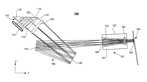
As shown in Figs. 1 and 2, such a fmgerprint imaging apparatus or system 100
includes an optical plate or platen 102, a primary lens 104, a mirror system
106, an
objective lens system 107, an image sensor system 108, and an illumination
source
110. For further reference, directions Yand Z of the orthogonal coordinate
system are
shown on Fig. 1 by arrows. A third direction Xof this orthogonal coordinate
system is
perpendicular to the drawing plane of Fig. 1.
5
CA 02585625 2007-04-27
WO 2006/050337 PCT/US2005/039415
The optical platen 102 includes an object receiving surface or finger field
112
located on its top. An object, such as a finger, to be identified is applied
to the surface
112. The surface 112 comprises the object plane of the system 100.
The finger field 112 has an optically smooth surface to provide good contact
with the finger skin ridges. The finger field regions that interface with the
finger skin
ridges and valleys form the fingerprint pattern. The finger field has
dimensions
sufficient for reliable identification of the fingerprint pattern. The object
receiving
surface is large enough to provide sufficient X-Y dimensions to image four
fingers at
the same time as well as rolled fingerprint images. The surface of the object
receiving
surface in the X-Y plane may, for example, be about 86 millimeters (mm) in
length
(the X-direction) and about 66 mm in width (the Y-direction).
The optical plate or prism 102 includes a first side surface 114 and a second
side surface 116 inclined to the finger field 112. The finger field and the
surfaces 114
and 116 are planar in shape. Other shapes are possible for either or both of
these
surfaces, such as, for example, cylindrical shapes, to enhance various
characteristics
of the fingerprint image.
The surface 114 is configured to receive a source of illumination for the
object
plane surface 112. The surface 116 is the viewing face through which the
illuminated
object plane is viewed by TIR. The surface 114 is inclined to the finger field
at an
angle 118, as shown in Fig. 1. The value of the angle 118 is generally chosen
to
accomplish the desired illumination of the object plane. The surface 116 is
inclined to
the finger field at an angle 120. The object plane surface 112 is illuminated
through
the illumination face 114 of the prism at an angle in the range of 25 to 40
degrees( ).
The angles 118 and 120, in one embodiment, may be approximately 40 and 50 ,
respectively. This embodiment represents bright field illumination. Dark field
illumination whereby the object plane is illuminated at an angle approximating
90
may also be utilized. In this case, the finger friction ridges are seen as a
bright object
on the dark field background. The dark field implementation may be preferable
in
some cases where packaging of the optics dictates that the illumination be
provided
from other than a front surface of the object plane prism or plate.
The primary lens104 is positioned external to the optical plate 102 and behind
its lateral surface 116. The primary lens 104 may comprise, for example, a
square
field lens. The field lens accomplishes telecentricity of rays at the object
plane. The
lens directs light from the object plane to the objective lens system 107.
6
CA 02585625 2013-03-14
77471-62
When a finger is applied to the object plane, finger ridge detail is viewed by
frustrated total internal reflection (Fall). The optical plate or prism in one
embodiment employs the principle of moisture discrimination whereby the index
of
the refraction of the glass and the viewing angle of the object plane can
discriminate
the index of refraction of skin from that of both air and water at the object
plane
surface. This technique is described in U.S. Patent No. 5,416,573, entitled
"Apparatus For Producing Fingerprint Images Which Are Substantially Free Of
Artifacts Attributable To Moisture On The Finger Being Imaged", assigned to
the
assignee of the subject application.
Specifically, in one embodiment, the image sensor system 108 receives light
from the platen surface where air or water is in contact with that surface,
but receives
significantly less light from regions of the platen surface where friction
ridge skin is
in contact. Generally, moisture discrimination is implemented with high index
of
refraction glass to implement TIR with acceptable geometric distortion. Lower
index
glass is also feasible with associated techniques to correct for geometric
distortion
and provide acceptable contrast transfer function (C1T) at the associated
steeper
viewing angle.
The prism may comprise SF-11 glass (index of refractiop = 1.785) readily
available from high quality glass fabricators. The viewing angle 120 is, in
one
embodiment, as noted, is approximately 50 to accomplish moisture
discrimination.
A lower index glass may be used, for example, BK7 glass, and the object plane
viewed at a lower angle, for example, at an angle of approximately 65 , to
accomplish
FTIR for skin and water applied to the object plane. Other transparent
materials, glass
or plastics, for instance, may be used in place of these specific glasses.
The mirror system 106 comprises two fold mirrors 118 and 120. The mirrors
may be folded at an angle of about 11 to shorten the optical path length. The
mirrors
reflect light, as shown, of a wavelength, such as about 450 to 650 nm,
produced by the
illumination source 110.
As shown in Fig. 2, the objective lens system 107 may comprise a pair of 2-
doublet achromats 121 and 122. In this embodiment, there are two doublets for
each
imager of the image sensor system 108. The objective or the achromat 121, as
shown
in Fig. 1, includes doublet lenses 123 and 124. The objective or the achromat
122
also includes two doublet lenses (not shown) configured in a similar fashion.
Each 2-
doublet objective functions as an achromatic lens, thereby removing a
substantial
7
CA 02585625 2007-04-27
WO 2006/050337 PCT/US2005/039415
portion of chromatic aberration. That is, the objective lenses provide lateral
and axial
color correction for the wavelengths of interest, for example, about 450 to
650 nm.
The lens mechanism 107 also provides a respective aperture stop 126 for each
objective that defines an aperture light beam of imaging light rays forming an
image
of a fingerprint pattern. Other color-corrected lens configurations may be
applied in
the objective lens to accomplish focus of the image onto the image plane
without
color aberration, for example, a six element objective comprising two
doublets, two
singlets, and an aperture stop to provide higher CTF over a wider field of
view.
The doublets may be mounted in a barrel arrangement 127. The barrel
arrangement may have a diameter of about 1.50 inches and a length of about 3
inches.
The object plane field of view (FOV) is thus mapped to the image sensor
system 108 through color corrected optics, including the fold mirrors. The
optics
configuration is telecentric at both the object plane and the image plane to
provide a
broad region of high optical performance, exhibiting small blur spots
throughout the
FOV for all colors. The vertical FOV, in various embodiments, may be between
about 2 and 4 inches.
In one embodiment, the image sensor system 108 comprises a pair of CMOS
image sensors 128 and 130. The image sensors are high-pixel density color
imagers.
The image sensors employed may be three megapixel CMOS devices manufactured
by Micron Semiconductor. Alternatively, the image sensors may use fewer than
or
more than three megapixels. Single imagers may be employed depending on the
horizonatal field of view to be imaged and the available imager horizontal and
vertical
pixels.
The image sensor or sensors provide digital output data at frame rates of
about
12 frames per second or greater. The frame rate is high enough to avoid
artifacts.
The sensors are tilted to accomplish Scheimpflug correction of trapezoidal
image
distortion and variation in focus in vertical FOV caused by the steep viewing
angle.
The sensor angle is between 2 and 110 and is a function of the object plane
viewing
angle 120. The sensors may be tilted, in one embodiment, at an angle of about
2.8
from the image axis. Each sensor views a portion of the total FOV. For
instance, in
the illustrated embodiment, each imager or sensor views approximately half of
the
total FOV.
8
CA 02585625 2007-04-27
WO 2006/050337 PCT/US2005/039415
The imager sensor or sensors may use a RGB (red-green-blue) color matrix or
a CMYG (cyan-magenta-yellow-green) color matrix. Also, color CCD imagers may
be used in place of the color CMOS imagers.
As shown in Fig. 1, the illumination source 110 is arranged and operated to
illuminate the finger field 112. The illumination source 110 is a multi-color
or non-
monochromatic light source. The illumination source, in one embodiment, may be
a
white light source producing light in the range, for example, of about 450 to
650 mn.
The illumination source, in other embodiments, may be a red and green; blue
and
green; cyan, magenta and green; cyan, green and yellow; or green, yellow, and
magenta light source. The illumination source may be radiation sources such as
light
emitting diodes (LEDs), cold cathode fluorescent tubes, or plasma light
panels.
As shown in Fig. 3, the illumination source may be a light pipe 132. The light
pipe includes light receiving surfaces 138 substantially orthogonal to a light
input
surface 134. The light output surface 136 is spaced from and substantially
parallel to
an outside light receiving or back surface 138. An open space or cavity 139 is
formed
between the light output surface 136 and the back surface 138.
The light pipe may be constructed of clear acrylic. The outside surface 138 of
the light pipe, opposite the light output surface, may be opaque white. For
example,
this surface may be painted or coated to be opaque. Internal surfaces of the
light pipe
are constructed to provide unifoim illumination of the painted surface.
A diffusing structure 140 is positioned at the output face 136 of the light
pipe.
The diffusing structure diffuses minute irregularities in the light output
from the
surface 136 and deflects undesirable light entering the system through the
object plane
away from the light pipe. The diffusing structure may comprise an array of
microprisms. The microprism array may be a Vikuiti Display Enhancement Film
available from the 3M Corporation, St. Paul, Minnesota. The microprism
structure
may be molded into the front face 136 of the light pipe. Alternatively, the
microprism
structure may be formed as a separate part foulm the surface 136.
The light source, in one configuration, includes LED devices 140 mounted in
respective reflecting end caps 142 mounted on or adjacent to the light pipe
light
receiving surfaces 134. The devices 140 are high output white (approximately
3000K) LEDs. The LEDs produces white light in the range, for example, of about
450 to 650 rim.
9
CA 02585625 2013-03-14
77471-62
The illumination source provides uniform illumination at the surface 112.
This reduces the amount of gain equalization necessary across the FOV, thereby
increasing signal to noise and ensuring high grayscale contrast. Additionally,
the
illumination scheme has the benefit of weakly imaging latent fingerprint ridge
residue
left on the object plane 112 by oil and other residue on the finger. Thus,
this
illumination scheme provides a relatively high contrast ratio with low noise.
The CMOS imager outputs are digital with output data corresponding to red
(R), green (G), and blue (B) components of the applied light. The white light
stimulates all ROB components with equal illumination, first order. Second
order
variations due to (1) illumination differences in the three primary colors,
(2) Bayer
filter losses, and (3) imager ROB channel gain imperfections are compensated
for by
first normalizing the ROB imbalances to accomplish equal outputs per channel
across
the dynamic range of the imagers followed by illumination equalization to
compensate for second order variations in the illumination profile.
As shown in Fig. 4, processing of image data, from imagers 108, derived from
imaging surface 112, is accomplished in a special purpose digital signal
processing
(DSP) computer 150. The computer 150 receives image output data 152 from the
fingerprint image sensors or imagers 128 and 130. This processed image data
conforms to the FBI specified requirements, for example, the FBI Appendix F
specifications. The processed images are outputted to a host computer (not
shown)
via an IEEE 1394 Firewire link 154 for assembly into a record comprised of a
set of
images and textual data. An image grab 156 of the computer 150 may be
implemented using a technique such as that described in U.S. Patent No.
5,748,766,
entitled "Method and Device for Reducing Smear in Rolled Fingerprint Image,"
or the
technique described in U.S. Patent No. 4,933,976, entitled "System for
Generating
Rolled Fingerprint Images", assigned to the assignee of the subject
application.
The computer 150 also controls, as represented by control box 158, the
operation of the image sensor system 108 and the illumination source 110. The
optics
of the imaging system 100 are represented by box 160.
In another embodiment, data may be transferred to the host computer prior to
processing into final fingerprint form. The final fmgerprint processing would
then be -
accomplished in software or a combination of hardware and software on the host
computer.
CA 02585625 2013-03-14
- 77471-62
Also, an optional hand scanner 162 may be used in conjunction with the
imaging system 100. The hand scanner operates under the control, control box
164,
of the computer 150. The computer receives image output data 166 from the hand
scanner 162. The hand scanner 162 may be of the type described in U.S. Patent
No.
6,175,407, entitled "Apparatus And Method For Optically Imaging Features On
The
Surface Of A Hand", assigned to the assignee of the subject application.
A number of implementations and techniques have been described. However,
it will be understood that various modifications may be made to the described
components and techniques. For example, advantageous results still could be
achieved if steps of the disclosed techniques were performed in a different
order, or if
components in the disclosed systems were combined in a different manner, or
replaced or supplemented by other components.
For example, the optical layout of the imaging system 100 may use only one
fold mirror or more than two mold mirrors. It is also possible, in one
embodiment, to
eliminate the fold mirrors entirely by either reducing the front and back
focal length
or the objective lens and/or packaging the optics system in a longer housing.
The
objective lens system may comprise some lens combination other than a pair of
doublets. For instance, a combination of three pairs of doublets may be used
to
provide higher CTF over a larger FOV. Also, objects other than a finger may be
imaged by the imaging device.
Additionally, instead of two imagers, only one imager may be employed. A
smaller prism could be used and the prism illuminated by an LED white light
source.
The FOV could be mapped to a single high-pixel density color CMOS imager
through
color corrected optics with magnification reduced to increase resolution. The
single
CMOS imager embodiment may also use a larger prism with magnification
increased
to yield a lower resolution image but over a much larger FOV. In another
configuration, the light source,as discussed, may be multi-color providing
more then
one wavelength of light through color-corrected optics to stimulate more than
one
pixel color at the CMOS or CCD imaging device. For example, a CMYG (cyan-
magenta-yellow-green) imager might be efficiently illuminated with a light
source
that would stimulate three of the four imager colors, but not the fourth. The
color
correction in the optics would be easier by virtue of the smaller spread of
wavelengths
11
CA 02585625 2013-03-14
- 77471-62
that would have to be supported and the illumination could be accomplished
with bi-
color LEDs.
A number of embodiments of the invention have been described.
Nevertheless, it will be understood that various modifications may be made
without
departing from the scope of the claims.
12