Note: Descriptions are shown in the official language in which they were submitted.
CA 02586235 2013-07-16
ELECTRO-ACTIVE SPECTACLES AND METHOD OF FABRICATING SAME
[0001] FIELD OF THE INVENTION
[0002] The present invention relates generally to spectacles and, in
particular to
spectacles comprising electro-active lenses.
[0003] SUMMARY OF THE INVENTION
[0004] An illustrative aspect of the invention provides a composite lens
assembly
comprising an electro-active lens assembly, a first lens wafer, and a second
lens wafer.
The electro-active lens assembly has an upper substrate layer with a planar
upper surface
and a lower substrate layer with a planar lower surface. The first lens wafer
has a planar
lower wafer surface adjacent and parallel to the planar upper surface of the
upper
substrate layer of the electro-active lens assembly. The second lens wafer has
a planar
upper wafer surface adjacent and parallel to the planar lower surface of the
lower
substrate layer of the electro-active lens assembly.
[0004a] In another aspect, the present invention provides a composite lens
assembly having a fixed lens, comprising:
a. an electro-active lens assembly; and
b. a first adhesive layer and a second adhesive layer, wherein said electro-
active lens assembly is disposed between said first and said second adhesive
layers, and
wherein at least one of said first and said second adhesive layers is adapted
for
securing said electro-active lens assembly to the fixed lens layer of the lens
assembly.
CA 02586235 2013-07-16
[000411] In another aspect, the present invention provides a composite lens
assembly, comprising:
a. a fixed focal length lens;
b. an electro-active lens assembly; and
c. a first adhesive layer and a second adhesive layer, wherein said electro-
active lens assembly is disposed between said first and said second adhesive
layers,
wherein at least one of said first and said second adhesive layers is adapted
for securing
said electro-active lens assembly to said fixed focal length lens of the lens
assembly and
wherein at least one of said first and said second adhesive layers is adapted
to adhere to
components which provide electricity to said electro-active lens assembly from
an
eyeglass frame.
[0004c] In another aspect, the present invention provides a composite lens
assembly, comprising: a fixed focal length lens; an electro-active lens
assembly; and an
adhesive layer, wherein said electro-active lens assembly is surrounded by
said adhesive
layer, wherein said adhesive layer is adapted for securing said electro-active
lens
assembly to said fixed focal length lens of the lens assembly and wherein said
adhesive
layer is adapted to cover a component which provides electricity to said
electro-active
lens assembly from an eyeglass frame.
[0004d] Accordingly, in one aspect the present invention resides in a
composite
lens assembly, comprising, in order: a first glass or plastic substrate, a
first electrode
layer, a first alignment layer, a liquid crystal layer comprising a spacer
surrounding a
liquid crystal material, a second alignment layer, a second electrode layer,
and a second
glass or plastic substrate, whereby an adhesive layer provides support for the
composite
lens assembly.
2
CA 02586235 2013-07-16
[0005] This and other aspects will become apparent from the following
description of the preferred embodiment taken in conjunction with the
following
drawings, although variations and modifications may be effected without
departing from
the spirit and scope of the novel concepts of the disclosure.
BRIEF DESCRIPTION OF THE DRAWINGS
[0006] The present invention can be more fully understood by reading the
following detailed description together with the accompanying drawings, in
which like
reference indicators are used to designate like elements.
[0007] Figure 1 is a section view of an electro-active lens assembly that may
be
used in or in conjunction with embodiments of the invention.
[0008] Figure 2 is a bottom view of the electro-active lens assembly of Figure
1.
[0009] Figure 3A is an expanded view of a composite lens assembly according to
an embodiment of the invention.
[0010] Figure 38 displays an assembled view of the composite lens assembly of
Figure 3A.
[0011] Figure 4A is an expanded view of a composite lens assembly according to
an embodiment of the invention.
2a
CA 02586235 2013-07-16
[0012] Figure 4B is an assembled view of the composite lens assembly of Figure
4A.
[0013] Figure 5 displays a composite lens assembly according to an embodiment
of the invention mounted inside of a spectacle frame.
2b
CA 02586235 2007-05-02
WO 2006/050366 PCT/US2005/039494
[0014] Figure 6 is a section view of an electro-active lens assembly that may
be used in or in
conjunction with embodiments of the invention.
[0015] Figure 7A is a bottom view of the electro-active lens assembly of
Figure 6.
[0016] Figure 7B is a top view of the electro-active lens assembly of Figure
6.
[0017] Figure 8A is an expanded view of a composite lens assembly according to
an
embodiment of the invention.
[0018] Figure 8B is an assembled view the composite lens assembly of Figure
8A.
DETAILED DESCRIPTION OF THE INVENTION
[0019] Hereinafter, various embodiments of the invention will be described. As
used herein,
any term in the singular may be interpreted in the plural, and alternately,
any term in the
plural may be interpreted to be in the singular. The terms "upper" and "lower"
refer merely
to the relative orientation of the elements as shown in a particular figure,
and do not imply
any required final orientation of the electro-active lens assembly relative to
the environment.
Similarly, the terms "first" and "second" are used merely for convenience, and
do not imply
any required final orientation or order of assembly.
[0020] Embodiments of the invention provide spectacles formed as composite
assemblies of
.electro-active lens elements and passive lens elements. As used herein, the
term "electro-
active lens" refers to a lens whose optical properties may be changed or
modified with the
application of electricity. Of particular interest are electro-active lenses
formed from liquid
crystal lens elements that may be configured for correction of any of a
variety of vision
problems.
[0021] The fabrication of a liquid crystal electro-active lens assembly and
the incorporation
of such a lens assembly into a composite lens assembly presents a number of
challenges. For
example, the structure of the electro-active lens element must be established
so as to control
the thickness of the liquid crystal layer and so as to allow edging (i.e.,
removal of material
around the edges) of the composite electro-active lens assembly. Edging of
lenses for
spectacles is very important because edging properly aligns and positions the
lenses (inside of
the spectacle frame) relative to the eyes.
[0022] Another challenge is that electrical communication must be established
among the
electrical components (e.g., driver chip, contacts and electrodes) of the
electro-active portion
of the composite lens assembly. As will be discussed, this may be done through
vias (small
3
CA 02586235 2007-05-02
WO 2006/050366 PCT/US2005/039494
holes) which may be perpendicular to the layers, and thus avoid the edge of
the electro-active
lens assembly. This internal electrical communication may be similar to multi-
layered
integrated circuit design, wherein multiple layers are physically separated,
but may
communicate with each other through vias as needed.
[0023] Yet another challenge is the physical integration of the electro-active
lens assembly
into the composite lens assembly. In some embodiments, the composite lens
assembly may
be secured (held together) using screws or bolts, and these screws or bolts
may serve as a
convenient electrical path for the power supply. In this case, the composite
lens assembly
may be edged for proper positioning inside of a spectacle frame.
[0024] Embodiments of the invention will now be discussed in more detail.
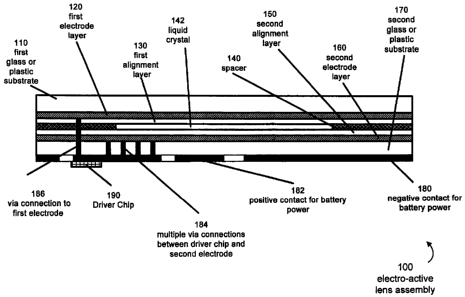
[0025] Figure 1 displays an electro-active lens element assembly 100 that may
be used in or
in conjunction with embodiments of the invention. The electro-active lens
assembly 100 is
particularly adapted for use in the composite lens assemblies discussed below.
The electro-
active lens assembly 100 is essentially a laminate structure with both power
contacts 180, 182
positioned on its lower surface. The layers of this laminate structure in
order from the upper
surface to the lower surface are:
= a first glass or plastic substrate 110,
= a first electrode layer 120,
= a first alignment layer 130,
= a liquid crystal layer comprising a spacer 140 surrounding a liquid
crystal 142,
= a second alignment layer 150,
= a second electrode layer 160,
= a second glass or plastic substrate 170,
= a contact layer comprising a positive contact 182 for battery power, and
a negative
contact 180 for battery power,
= a driver chip 190.
[0026] The driver chip 190 is connected to the first electrode layer 120
through a via
connection 186, and the driver chip 190 is also connected to the second
electrode layer 160
through multiple via connections 184.
[0027] The driver chip 190 may be positioned in another layer, for example
inside of second
glass or plastic substrate 170 with appropriate via connections to other
elements. Alternately,
4
CA 02586235 2007-05-02
WO 2006/050366
PCT/US2005/039494
the drive chip 190 may be positioned on the same layer as the second electrode
layer, in order
to minimize the number of necessary vias.
[0028] The first glass or plastic substrate 110, which may be referred to as
the upper substrate
110, may be substantially flat on both the upper side and the lower side. The
first glass or
plastic substrate 110 may provide structural support for the other elements,
and may provide
electrical insulation for the other elements. The substantially flat lower
side of the upper
substrate 110 is adjacent to the substantially flat upper side of first
electrode layer 120.
[0029] The first electrode layer 120 may be a solid electrode, and may serve
as a reference
electrode relative to the second electrode layer 160. The substantially flat
lower side of first
electrode layer 120 may serve as a substrate to attach alignment layer
molecules. The lower
side of the first electrode layer 120 is adjacent to the substantially flat
upper side of the first
alignment layer 130.
[0030] The first alignment layer 130 comprises materials that aid the
alignment of the liquid
crystal layer 142. The substantially flat lower surface of first alignment
layer 130 is adjacent
to liquid crystal 142 and spacer 140.
[0031] The optical properties of liquid crystal 142 may be changed by electric
and magnetic
fields. Alternately, the spacer 140 may be thicker than shown in Figure 1, and
may encircle
all of the following: the first alignment layer 130, the liquid crystal 142,
and the second
alignment layer 150. The substantially flat lower side of liquid crystal layer
142 is adjacent
to the substantially flat upper side of the second alignment layer 150.
[0032] Note that material may be removed from around the edge of the electro-
active lens
assembly without contacting or destroying the liquid crystal 142.
Specifically, some of the
spacer 140 may be removed or edged without contacting or destroying liquid
crystal 142.
[0033] The second alignment layer 150 comprises materials that aid the
alignment of the
liquid crystal layer 142. The substantially flat lower side of alignment layer
150 is adjacent
to the substantially flat upper side of second electrode layer 160.
[0034] The second electrode layer 160 may be solid, or may be segmented or
patterned. For
example, the second electrode layer 160 may be individually controlled pixels
patterned into
an arbitrary array, or may be patterned into other useful patterns such as a
set of concentric
circles. The multiple via connections 184 from the driver chip 190 may
individually control
the pixels or patterns. Note that the first electrode layer 120 may serve as a
reference
electrode in contrast to any voltages on the second electrode layer 160. The
electric field
CA 02586235 2007-05-02
WO 2006/050366 PCT/US2005/039494
created between the second electrode layer 160 and the first electrode layer
120 may affect
the optical qualities (such as index of refraction or transmissivity) of the
liquid crystal 142.
The electrodes 120 and 160 may have spacers around them in order to insulate
them from the
edge, and in order to allow edging of the electro-active lens assembly 100.
The substantially
flat lower side of the second electrode 160 is adjacent to the substantially
flat upper side of
the second glass or plastic substrate 170.
[0035] The second glass or plastic substrate 170, which may be referred to as
the lower
substrate 170 may provide structural support for the other elements, and may
provide
electrical insulation for the other elements. The substantially flat lower
side of the lower
substrate 170 is adjacent to the substantially flat upper side of positive
contact for battery
power 182 and negative contact for battery power 180. In this embodiment, the
positive
contact 182 and negative contact 180 are on the same layer, but are not
conductively attached
directly together. Both contacts are conductively attached to the driver chip
190. ,
Additionally, one of the contacts may be directly attached to the first
electrode layer 120, and
may serve as a reference for the second electrode layer 160.
[0036] The driver chip 190 may be physically attached to the second glass or
plastic substrate
170, and may be conductively attached to the positive contact 182 and the
negative contact
180. Further, there may be additional contacts (not shown) for conductive
control signals,
and there may be an antenna (not shown) for wireless signals. Alternately,
control signals
may be piggybacked onto the power supply voltage.
[0037] The electrode, alignment and liquid crystal layers combine to form an
electro-active
cell that is held between the upper and lower substrate layers. It will be
understood that
additional layers may also be included in the electro-active cell.
[0038] In some embodiments, the electrode layers 120 and 160 are formed on
thin parallel
glass or plastic sheets or slides and are covered with the alignment layers
130 and 150 to
orient the molecules in the liquid crystal material. One or more of the
electrodes may be
patterned to allow for the designed optical effect. For example, if purely
spherical power is
required, then the pattern may comprise of a set of individually addressable
concentric ring
electrodes. If phase wrapping is used, the electrodes may be ganged or grouped
to reduce the
number of contacts needed to drive the lens. If a general or arbitrary optical
effect is desired,
for example a wave front correction for higher order aberrations, then the
individually
addressable pattern may comprise a Cartesian grid. The spacers 140 may be used
to create a
6
CA 02586235 2007-05-02
WO 2006/050366 PCT/US2005/039494
constant gap thickness that is filled with liquid crystal or other electro-
active material. A
driver chip may be mounted on one side of the electro-active lens assembly and
electrical
contacts are made through a group of vias drilled or cut or etched in the
glass or plastic
substrate.
[0039] If a polarization dependent nematic liquid crystal is used, then two
electro-active lens
assemblies like the one shown above may be stacked and oriented at a 90-degree
angle to
eliminate the effects of birefringence.
[0040] Alternatively, the solid electrode 120 may be converted to a patterned
electrode and a
common reference electrode placed in the center of the cell with a liquid
crystal layer on each
side of the common electrode. The common electrode may be constructed from a
thin piece
of glass or optical grade plastic coated with a transparent conductor on each
side. The
alignment layers on the two patterned electrodes may be oriented at 90-degrees
from one
another. In some embodiments, it may also be desirable to place an alignment
layer on each
side of the common electrode, which would be applied over the transparent
conductor layers
making up the common electrode, and oriented at 90-degree angles with one
another. It will
be understood that if a common reference electrode is added to the cell, one
or more
additional conductors/vias may be added to allow voltage application from the
driver circuit
to the new patterned electrode. Additional vias may also be used to make
electrical contact
between the new common electrode and the driver circuit.
[0041] If a cholesteric liquid crystal is used, then only a single cell will
be required to
produce the optical power. For the sake of simplicity we will limit the
present discussion to
cholesteric liquid crystal designs, with the understanding that the techniques
described herein
are applicable to nematic liquid crystal designs as well.
[0042] Figure 2 is a bottom view of the electro-active lens element 100
showing an
illustrative configuration for the electrical contacts 180, 182. The contacts
180, 182 may be
formed from a mostly or fully transparent conductive material such as, by way
of example
only, ITO. As shown in Figure 2, the negative contact 180 may be configured to
cover a
substantial area, and may connect through a bus to the driver chip 190. The
positive contact
182 may also cover a substantial area and may connect through a bus to the
driver chip 190.
The driver chip 190 may be mounted in an area free of electrically conductive
material
(except the positive and negative buses), so that the various output pins (not
shown) of the
driver chip will not be shorted out. In this manner, power from a battery or
other power
7
CA 02586235 2007-05-02
WO 2006/050366 PCT/US2005/039494
source, can be provided to the chip 190 and for powering the electro-active
lens 100, by
simply making an electrical contact to the positive contact 182 and negative
contact 180 of
the electro-active lens assembly 100. Other geometric layouts of the
electrical contacts may
prove convenient, and the chip 190 may be moved to other locations.
[0043] It will be understood by those of ordinary skill in the art that
although one contact is
designated as a positive contact and one is designated a negative contact, the
positive and
negative polarity may be reversed.
[0044] With reference to Figures 3A and 3B, an illustrative embodiment of the
invention
combines an electro-active lens element of the type described above in Figures
1 and 2 with a
pair of lens wafers to produce a composite lens assembly 300 having a fixed or
base power.
[0045] Figure 3A displays an expanded view of the composite lens assembly 300.
The
elements of the composite lens assembly are:
= a front lens wafer 310,
= a first adhesive layer 320,
= an electro-active lens 330 (for example, the electro-active lens
described in Figures 1
and 2),
= a positive battery terminal wire 340 and a negative battery terminal wire
350,
= a second adhesive layer 322, and
= a back lens wafer 360.
[0046] The front lens wafer 310 may have.a substantially flat lower surface.
Alternately, the
interior lower surface of the front lens wafer 310 may be curved to match a
curved electro-
active lens assembly. The front lens wafer 310 may be constructed from glass
or optical
grade plastics, such as, by way of example only, CR39, polycarbonate, or high
index
polymers. The front lens wafer 310 may be constructed from different materials
than the
back lens wafer, for example one from glass and one from plastic. The front
lens wafer 310
may have substantially flat upper and lower surfaces, and thus have piano (or
null) refractive
power. The upper surface of front lens wafer 310 may be curved, and thus
create refractive
power. The substantially flat lower surface of front lens wafer 310 is
adjacent to the
substantially flat first adhesive layer 320.
[0047] The first adhesive layer 320 may be flexible or rigid, and may be index-
matched, the
index of refraction may be matched to the index of refraction of the adjacent
wafer. The
8
CA 02586235 2007-05-02
WO 2006/050366 PCT/US2005/039494
substantially flat lower surface of first adhesive layer 320 is adjacent to
the substantially flat
electro-active lens assembly 330.
[0048] The electro-active lens assembly 330 may be or comprise the electro-
active lens
assembly 100 as shown in Figure 1, for example. The substantially flat lower
side of electro-
active lens assembly 330 may have a positive contact area and a negative
contact area as
shown in Figure 1 and in Figure 2. These contact areas are positioned adjacent
to the upper
surface of positive battery terminal wire 340 and the upper surface of
negative battery
terminal wire 350. Said wires may also be flat strips. Said wires may be
attached to alternate
power sources, such as storage capacitors or solar cells.
[0049] Alternately, in one embodiment (not shown) the electro-active lens
assembly 330 may
have a smaller diameter than the lens wafers 310 and 360, and also may have a
smaller
diameter than lens the adhesive layers 320 and 322. In this embodiment, the
adhesive layers
would be squeezed around the electro-active lens assembly, and would
effectively
encapsulate it. In this embodiment, material may be removed from around the
edge of the
composite lens assembly 300 without contacting or destroying the contacts or
the liquid
crystal of the electro-active lens assembly 330. Thus, in this embodiment the
composite lens
assembly 300 may be capable of being edged.
[0050] Alternately, in another embodiment (not shown), the electro-active lens
assembly 330
may have a smaller diameter than the lens wafers, and may be surrounded by a
spacer. Thus,
in this embodiment the composite lens assembly 300 may be capable of being
edged.
[0051] The positive battery terminal wire 340 may terminate in a flat strip
with an area
corresponding to and aligned with the positive contact area (for example,
contact area 282 as
shown in Figure 2) of the electro-active assembly 330. Negative battery
terminal wire 350
may terminate in a similar fashion. The lower surface of positive battery
terminal wire 340
and the lower surface of negative battery terminal wire 350 are adjacent to
substantially flat
upper surface of the second adhesive layer 322.
[0052] The second adhesive layer 322 is similar in form and function to the
upper adhesive
layer 320. The substantially flat lower surface of the second adhesive layer
322 is adjacent to
the substantially flat upper surface of back lens wafer 360.
[0053] Note that the second adhesive layer may deform about the battery
terminal wires so as
to fill the spaces between the battery terminal wire 340 and battery terminal
wire 350, and
thus effectively provide a single layer with substantially flat sides.
9
CA 02586235 2007-05-02
WO 2006/050366
PCT/US2005/039494
[0054] Additionally, note that the battery terminal wires 340 and 350 may be
routed
approximately perpendicularly downward through vias (not shown) in the second
adhesive
layer 322 and vias (not shown) in the back lens wafer 360. When the wires 340
and 350 are
routed perpendicularly, and when the diameter of the electro-active lens
assembly is reduced
(as discussed above), then the composite lens assembly 300 may be edged.
[0055] Edging is a well known technique in the art of optics wherein a lens
(or the composite
lens assembly 300) has material removed from the edge in order to properly
position the
edged lens inside of a frame relative to the environment. For example,
typically an
optometrist or optician positions an empty spectacle frame on the patient's
face, then makes
several measurements, and then edges a lens so that it is properly positioned
and aligned
inside of the spectacle frame relative to the patient's eye.
[0056] The back lens wafer 360 is similar in form and function to the front
lens wafer 310.
Together, the front lens wafer 310 and the back lens wafer 360 may provide a
fixed or base
refractive power to the total optical power of composite lens assembly 300.
Alternately, the
wafers may be plano (have no optical power), and merely serve structural
purposes.
[0057] Figure 3B displays an assembled view of the composite lens assembly 300
with a
fixed or base power. Specifically, Figure 3B shows the individual elements of
Figure 3A in
an assembled or compressed view. The adhesive layers 320 and 322 hold the
composite lens
assembly 300 together.
[0058] With reference to Figures 4A and 4B, an illustrative embodiment of the
invention
combines an electro-active lens element of the type described above in Figures
1 and 2 with a
pair of lens wafers to produce a composite lens assembly 400 having a fixed or
base power.
Further, Figures 4A and 4B introduce screws or fasteners 470 to provide
additional
mechanical strength to the composite lens. Note that the adhesive layers
become optional
when the screws or fasteners are introduced.
[0059] Figure 4A displays an expanded view of an embodiment of a composite
lens assembly
400 with a fixed or base power and with screws or fasteners. The layers are:
= a front lens wafer 410,
= an first adhesive layer 420,
= an electro-active lens assembly 430 (for example, the electro-active lens
described in
Figure 1),
= a positive battery terminal wire 440 and a negative battery terminal wire
450,
CA 02586235 2007-05-02
WO 2006/050366 PCT/US2005/039494
= a second adhesive layer 422, and
= a back lens wafer 460.
[0060] Additionally, note the screw or fastener 470 and the nut or fastener
480 may be used
to add additional support to the composite lens assembly. Screws or fasteners
may be
particularly useful in rimless spectacle frames, because the screw or fastener
may be attached
directly to the rimless spectacle frames. In some embodiments the screw or
fastener may
serve as a conductive path in place of a battery terminal wire. Also, these
mounting screws
or fasteners may be used to secure the electro-active lens assembly 400 to a
spectacle frame
(not shown). The first adhesive layer 420 and second adhesive layer 422 are
optional because
the screw or fastener 470 and the nut or fastener 480 may provide adequate
support for the
composite lens assembly 400. Additionally, the positive battery terminal wire
440 and
negative battery terminal wire 450 are optional because the power may be
conducted through
the fasteners 470 and 480.
[0061] Routing the power through the screws or fasteners provides additional
benefits.
Specifically, if the electro-active lens assembly has a smaller diameter than
the wafers (and
possibly surrounded by a spacer as discussed above), then the composite lens
assembly 400 is
capable of being edged.
[0062] Edging is a well known technique in the art of optics wherein a lens
(or the composite
lens assembly 400) has material removed from the edge in order to properly
position the
edged lens inside of a frame relative to the environment. For example,
typically an
optometrist or optician positions an empty spectacle frame on the patient's
face, then makes
several measurements, and then edges a lens so that it is properly positioned
and aligned
inside of the spectacle frame relative to the patient's eye. Edging composite
lens assembly
400 (with power routed through the screws or fasteners) would not damage any
electrical
connections, and would not damage the liquid crystal. With the exception of
the screw or
fastener 470 and the nut or fastener 480, the other elements are the same as
those previously
described with respect to Figure 3A composite lens assembly 300.
[0063] Figure 4B displays an assembled view of the composite lens assembly 400
with a
fixed or base power, and including screws or fasteners.
[0064] Figure 5 displays an embodiment of a composite lens assembly 510
mounted inside of
a spectacle frame 500. The composite lens assembly 510 may, for example, be
similar to the
11
CA 02586235 2007-05-02
WO 2006/050366 PCT/US2005/039494
composite lens assembly 300 of Figures 3A and 3B may be mounted inside of
spectacle
frame 500.
[0065] Specifically, in Figure 5 positive terminal wire 540 and negative
terminal wire 550
electrically connect the electro-active lens assembly to a power supply such
as a battery 570
attached to a frame stem 560. The wires (540 and 550) may be light gauge
wires, or may be
conductive strips.
[0066] The frame in Figure 5 is a hinge-free design, but a hinged frame can
also be used
without deviating from the scope of the present invention. While the figure
illustrates
placement of the battery or power source on the frame stem, the power source
may also be
placed in or on the lens, adjacent to the lens, on or inside the bridge, nose
pad, hinge, or
where the hinge meets the frame front, which would potentially allow for
shorter connections
between the power source and the lenses. However, if the battery is relatively
large, then one
comfortable battery placement may be where the spectacle frame stem rests upon
the ear, so
that the ear carries the weight. The power supply may comprise a battery, a
capacitor, a solar
cell, or some combination of these power sources. For example, a solar cell
may charge a
capacitor. Further, the mechanical power of folding closed or opening the
spectacle frame
stem may be used to charge a battery or a capacitor.
[0067] Figure 6 illustrates an embodiment of an electro-active lens assembly
that is similar to
the embodiment in Figure 1. However, the electro-active lens assembly 600 of
Figure 6 has
positioned the positive contact on the bottom and the negative contact on the
top, in contrast
to the electro-active lens assembly 100 of Figure 1 which has positioned both
contacts on the
bottom. Changing the position of the contacts requires changing the position
of the vias, as
illustrated in Figure 6.
[0068] Specifically, Figure 6 displays a side view an embodiment of an electro-
active lens
assembly 600 with poSitive contact on the bottom and with negative contact on
the top. The
layers are:
= a negative contact for battery power 680,
= a first glass or plastic substrate 610,
= a first electrode layer 620,
= an first alignment layer 630,
= a liquid crystal layer 642, and a spacer 640,
= an second alignment layer 650,
12
CA 02586235 2007-05-02
WO 2006/050366
PCT/US2005/039494
= a second electrode layer 660,
= a second glass or plastic substrate 670,
= a positive contact for battery power 682, and
= a driver chip 690.
[0069] Additionally, note a via connection 686 to the first electrode layer
620, and an ultra
thin wire via connection 688 to the negative contact for battery power 680,
and multiple
through hole via connections 684 between the driver chip 690 and the patterned
electrode
layer 660. Electrical contacts through the various vias may be made with
transparent
conductors such as ITO, that can be deposited during iterative lithographic
steps, or by ultra
thin metal wires, designed for minimizing any adverse cosmetic effects.
[0070] Note that the battery contacts 680 and 682 are physically separated and
placed on the
top and bottom of the electro-active lens respectively. This physical
separation decreases the
possibility of short circuits, and simplifies placing the terminal wires.
[0071] Thus, the electro-active lens assembly 600 is almost identical to the
electro-active lens
assembly 100 shown in Figure 1, except for the relocation of the negative
contact for battery
power to the opposite side of the electro-active lens assembly, and except for
the new related
via 688.
[0072] Figures 7A and 7B illustrate bottom and top views of the electro-active
lens element
600 from Figure 6, showing an illustrative configuration for the electrical
contacts 680 and
682.
[0073] Specifically, Figure 7A displays the underside of the electro-active
lens assembly 600
which shows the positive contact 682 which is connected to a driver chip 690.
Figure 7B
shows the top of the electro-active lens assembly 600 which shows the negative
contact 680.
The negative contact 680 is connected to the driver chip 690 through a wire
via 688. As
shown in Figure 6, the via 688 passes through the upper substrate 610, the
first electrode
layer, the spacer 640 in the liquid crystal layer, the second electrode layer
660 and the lower
substrate 670 to the driver chip 690. The electro-active lens assembly 600 may
be powered
or charged through the positive contact 682 and negative contact 680. In
addition to power,
the positive contact 682 and the negative contact 680 may carry an embedded
control signal
to communicate with the driver chip 690.
13
CA 02586235 2007-05-02
WO 2006/050366 PCT/US2005/039494
[0074] With reference to Figures 8A and 8B, an illustrative embodiment of the
invention
combines an electro-active lens assembly of the type described above in
Figures 6 and 7 with
a pair of lens wafers to produce a composite lens assembly 800 having a fixed
or base power.
[0075] Figure 8A displays an expanded view 800 of an embodiment of a composite
lens
assembly with an electro-active lens assembly that has battery contacts on
opposite sides.
From top to bottom, Figure 8A displays:
= a front lens wafer 810,
= a first adhesive layer 820,
= a negative battery terminal wire or strip 850,
= an electro-active lens assembly 830 with battery contacts on opposite
sides (like
electro-active lens assembly 600 in Figure 6),
= a positive battery terminal wire or strip 840,
= a second adhesive layer 822, and
= a back lens wafer 860.
[0076] The composite lens assembly 800 is similar to composite lens assembly
300 in Figure
3A, except that the position of the negative battery terminal wire has been
moved to the
opposite side of the electro-active lens assembly 830 to follow the movement
of the negative
contact to the upper side of the electro-active lens assembly 830. Thus, the
composite lens
assembly 800 has battery terminal wires separated by the body of the electro-
active lens
assembly 830. This separation allows (but does not require) the battery
terminal wires to exit
the composite lens assembly 800 in the same radial direction. For example, in
Figure 8A
both battery terminal wires exit to the left, and may be easily ganged
together or joined into a
bus.
[0077] Although not shown, composite lens assembly 800 may be joined by
fasteners or
screws, and the fasteners or screws may be used to conduct the electrical
power.
[0078] Figure 8B displays an assembled view of the composite lens assembly 800
with the
negative battery terminal wire near the positive battery terminal wire.
[0079] While the geometries discussed herein and illustrated in the figures
are flat, it is
conceivable that curved parallel surfaces could also be employed that would
allow for thinner
composite lenses to be fashioned by the assembly methods described herein. In
embodiments
where the electro-active lens assembly is curved, one of the two wafers may be
eliminated as
14
CA 02586235 2007-05-02
WO 2006/050366 PCT/US2005/039494
the electro-active lens assembly would provide one of the two curved surfaces
required to
complete the distance vision optical power.
[0080] It will be readily understood by those persons skilled in the art that
the present
invention is susceptible to broad utility and application. Many embodiments
and adaptations
of the present invention other than those herein described, as well as many
variations,
modifications and equivalent arrangements, will be apparent from or reasonably
suggested by
the present invention and foregoing description thereof, without departing
from the substance
or scope of the invention.
[0081] While the foregoing illustrates and describes exemplary embodiments of
this
invention, it is to be understood that the invention is not limited to the
construction disclosed
herein. The invention can be embodied in other specific forms without
departing from the
spirit or essential attributes.