Note: Descriptions are shown in the official language in which they were submitted.
CA 02586966 2007-05-09
WO 2006/053129 PCT/US2005/040744
METHOD AND APPARATUS FOR FORMING A THIN-FILM SOLAR CELL
USING A CONTINUOUS PROCESS
CROSS-REFERENCE TO RELATED APPLICATIONS
[00011 This application claims priority from U.S. Provisional Patent
Application Ser. No.
60/626,843, filed November 10, 2004.
BACKGROUND OF THE INVENTION
[0002] The invention disclosed herein relates generally to the field of
photovoltaics and more
specifically to manufacturing thin-film solar cells using a continuous process
and thin film solar
cells made according to the process.
DESCRIPTION OF THE RELATED ART
[0003] Photovoltaic (PV) cells, modules and power systems offer clean,
reliable, renewable
energy to the world's expanding demand for electrical power. Unfortunately,
product costs have
not been sufficiently reduced to open up the critical markets in the
developing world where
electricity demand is driving them to polluting, non-renewable sources such as
coal and oil.
With the population expanding, and per-capita energy consumption going up, the
world is
heading towards an irreconcilable future where energy demand and supply
irreversibly diverge.
[0004] PV cells offer an alternative to non-renewable energy sources. However,
although
relatively efficient PV cells can be manufactured in the laboratory, it has
proven difficult to scale
into commercial scale processes with consistent repeatability and efficiency
critical for
commercial viability. The lack of an efficient thin-film manufacturing process
has contributed to
the failure of PV cells to effectively replace alternate energy sources in the
market.
CA 02586966 2007-05-09
WO 2006/053129 PCT/US2005/040744
[0005] Currently, cells are manufactured using a multi-step batch process
wherein each
product piece is transferred between reaction steps and such transfer is bulky
and requires
reaction in chambers to be cycled. A typical process consists of a series of
individual batch
processing chambers each specifically designed for the formation of various
layers in the cell.
One drawback to this process is that the substrate is transferred from vacuum
to air and back to
vacuum several times. An alternate system uses a series of individual batch
processing chambers
coupled with a roll-to-roll continuous process for each chamber. The major
drawback in this
process is the discontinuity of the system and the need to break vacuum.
[0006] Using approaches as outlined above, one or more defects can render the
entire plate (a
single device) useless and result in zero yield for that unit of product.
These and other problems
have relegated thin-film technologies to less than 10% market share worldwide.
SUMMARY OF THE INVENTION
[0007] The present invention provides a photovoltaic produced by providing a
substrate
mounted to a pallet through a series of reaction chambers where sequentially a
barrier layer, a
back contact layer, an semiconductor layer or layers, an n-type junction
buffer layer, an intrinsic
transparent oxide layer, a transparent conducting oxide layer and a top metal
grid can be formed
on the pallet.
[0008] In an alternate embodiment of the invention, a thin-film solar cell is
formed using a
continuous manufacturing process. In this embodiment, a flexible and
continuous substrate is
processed through a reactor having a plurality of process zones disposed along
a continuous path
between an entrance and exit of the reactor. Each process zone within the
reactor is defined by a
predetermined processing environment and is dedicated to one step layer of
device formation.
-2-
CA 02586966 2007-05-09
WO 2006/053129 PCT/US2005/040744
Each zone may further comprise processing conditions in conjunction with one
or more
deposition methodologies.
[00091 A method is further disclosed for forming a photovoltaic device in a
continuous
fashion. In this embodiment, a continuous substrate is passed at a defined
rate through a reactor
having a plurality of processing zones, wherein each zone is dedicated to one
production step
stage of device manufacture. These production steps include: 1.) A load or
isolation zone for
substrate preparation; 2.) an environment for depositing a barrier layer; 3.)
an environment for
depositing a back contact layer; 4.) an environment for deposition of a
semiconductor layer; 5.)
an environment for depositing alkali materials; 6.) an environment for
depositing another
semiconductor layer or layers; 7.) an environment for the thermal treatment of
one or more of the
previous layers; 8.) an environment for the deposition of an n-type
semiconductor layer wherein
this layer serves as a junction buffer layer; 9.) an environment for
deposition of an intrinsic
transparent oxide layer; and 10.) an enviroiunent for deposition of a
conducting transparent oxide
layer. In a fiu-ther embodiment, the process may be adjusted to comprise fewer
zones in order to
fabricate a thin film solar cell having fewer layers, or additional processing
can be added as well.
[0010] It is also understood that additional zones may be employed to isolate
deposition or
treatment zones from one another to prevent chemical cross-contamination and
to allow optimal
recovery. These isolation zones can range in the duration the work piece
resides therein in order
to allow the exposed substrate to reach an optimal condition for the next
production step in a
vacuum seal to prevent cross-contamination.
[0011] Depending upon the specific photovoltaic design, one or more zones
within the reactor
may be adjusted. For example, one or more zones comprising compatible
deposition
-3-
CA 02586966 2007-05-09
WO 2006/053129 PCT/US2005/040744
environments may be combined. Alternatively, a zone may comprise a combination
of
deposition processes enabling varying deposition environments or sub-zones.
[0012] In a further embodiment, one or more layers may be combined into a
single layer and
deposited in a single zone. For example, the semiconductor layer and the
alkali materials may be
combined to form an alkali containing mixed phase semiconductor source layer.
BRIEF DESCRIPTION OF THE DRAWINGS
[0013] FIG. 1 shows an embodiment of a thin-film solar cell produced by the
production
technology of the present invention.
[0014] FIG. 2 shows an embodiment of a continuous process for manufacturing a
thin-film
solar cell in accordance with the present invention.
[0015] FIG. 3 illustrates one embodiment of a substrate being fed from left to
right through a
continuous process in accordance with the present invention.
[0016] FIG. 4 illustrates one embodiment of a continuous process in accordance
with the
invention.
[0017] FIG. 5 illustrates another embodiment of a continuous process in
accordance with the
invention wherein zones further comprise one or more sub-zones.
[0018] FIG. 6A shows an embodiment of the processing method wherein two
substrates are
fed and processed simultaneously by a sequential sputter-evaporate process in
accordance with
the present invention.
[0019] FIG. 6B shows a top view of an embodiment of the processing method
wherein two
substrates are fed and processed simultaneously by a sequential sputter-
evaporate/sputter-
evaporate process.
-4-
CA 02586966 2007-05-09
WO 2006/053129 PCT/US2005/040744
[0020] To clarify, each drawing includes reference numerals. These reference
numerals
follow a common nomenclature. The reference numerals will have three or four
digits. The first
one or two digits represent the drawing number where the reference numeral was
first used. For
example, a reference numeral used first in drawing one will have a number like
1XX while a
number first used in drawing five will have a number like 5XX. The second two
numbers
represent a specific item within a drawing. One item in FIG. 1 will be 101
wliile another item
will be 102. Like reference numerals used in later drawing represent the same
item.
DETAILED DESCRIPTION OF THE INVENTION
[0021] The present invention employs a new production apparatus in order to
produce
photovoltaic devices. The particular apparatus will depend upon the specific
photovoltaic device
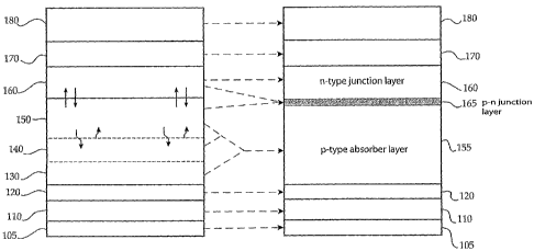
design, which can be varied. FIG. 1 shows a photovoltaic device or thin-film
solar cell 100
coinprising a substrate 105, a barrier layer 110, a back contact layer 120, a
semiconductor layer
130, alkali materials 140, another semiconductor layer 150, an n-type junction
buffer layer 160,
an intrinsic transparent oxide layer 170, and a transparent conducting oxide
layer 180. It will be
recognized by one skilled in the art that the thin film solar cell may
comprise fewer layers and
still function according to the invention. For instance, the device need not
have alkali-materials.
[0022] Two variations of an integrated production apparatus are provided. In
each case, a
series of treatment chambers are provided, where each chamber provides a
specific treatment
regimen in order to produce a specific layer deposition or layer treatment.
Each of these
treatment chambers allow a means to transport the work piece being made into
the photovoltaic
device to be transported from the first designed chamber, through the
sequential plurality of
chambers, until the work piece has been made into the designed photovoltaic
stack.
-5-
CA 02586966 2007-05-09
WO 2006/053129 PCT/US2005/040744
[0023] This plurality of reaction or treatment chambers provided with a
transport mechanism
may also include one or more isolation chambers that insure that particularly
effective reactants
are maintained in specifically desired chambers and do not contaminate
downstream processes.
Of course this isolation system is particularly important in the formation of
the semiconductor
layers of the photovoltaic device where relatively small amounts of material
determine whether a
layer is a p-type or n-type semiconductor. This carrier may be configured with
referencing
means to insure that the positioning of the work pieces are positioned within
the production
apparatus at defined positions.
[0024] The invention envisions two types of transport mechanisms for
transporting work
pieces through the apparatus. The first is a continuous roll system where a
relatively flexible
substrate is run through the system and collected. After finishing the stack
the substrate may be
cut into smaller pieces or, if the photovoltaic stack design permits, it may
be collected on a
finished roll.
[0025] The second approach is to provide a plurality of work piece substrates
onto a device
capable of fixturing the substrates onto a carrier that also has means that
allow the pieces to be
advanced in a precise fashion through the production apparatus.
[0026] Viewing FIG. 1, all layers are deposited on a substrate 105 which may
comprise one
of a plurality of functional materials, for exainple, glass, metal, ceramic,
or plastic. Deposited
directly on the substrate 105 is a barrier layer 110. The barrier layer 110
comprises a thin
conductor or very thin insulating material and serves to block the out
diffusion of undesirable
elements or compounds from the substrate to the rest of the cell. This barrier
layer 110 may
comprise chromium, titanium, silicon oxide, titanium nitride and related
materials that have the
requisite conductivity and durability. The next deposited layer is the back
contact layer 120
-6-
CA 02586966 2007-05-09
WO 2006/053129 PCT/US2005/040744
comprising non-reactive metals such as molybdenum. The next layer is deposited
upon the back
contact layer 120 and is a p-type semiconductor layer 130 to iinprove adhesion
between an
absorber layer and the back contact layer 120. The p-type semiconductor layer
130 may be a I-
IIIa,b-VI isotype semiconductor, but the preferred composition is Cu:Ga:Se,
Cu:AI:Se, or
Cu:In: Se alloyed with either of the previous compounds.
[0027] In this embodiment, the formation of a p-type absorber layer involves
the
interdiffusion of a number of discrete layers. Ultimately, as seen in FIG. 1,
the p-type
semiconductor layers 130 and 150 combine into a single composite layer 155
which serves as the
prime absorber of solar energy. In this embodiment, alkali materials 140 are
added for the
purpose of seeding the growth of subsequent layers as well as increasing the
carrier
concentration and grain size of the absorber layer 155, thereby increasing the
conversion
efficiency of the solar cell.
[0028] The alkali materials 140 are commonly sodium based and is usually
deposited in the
form of Na-VII (VII = F, Cl, Br) or Na2-VI (VI = S, Se, Te). When deposited,
the alkali
materials 140 may be in the form of a Na-A:I-III-VI alloy (A = VI or VII) to
allow for exchange
of elements with the semiconductor layer 150.
[0029] As shown by FIG. 1, the alkali material is discrete, and the
semiconductor layer 150 is
deposited upon it. However, the alkali materials do not stay discrete, but
rather are absorbed by
the semiconductor layer 150 as part of the formation of the final p-type
absorber layer as shown
in 155. When deposited, the alkali materials are deposited onto the p-type
semiconductor layer
130 or other preexisting layer through evaporation, sputtering, or other
deposition methods
known to those skilled in the art. In the preferred embodiment, the alkali
material 140 is
-7-
CA 02586966 2007-05-09
WO 2006/053129 PCT/US2005/040744
sputtered at ambient temperature and at a mild vacuum, preferably 10-6 - 10-2
torr. Once
deposited, the layers are tllermally treated at a temperature of about 400 C -
600 C.
[0030] After the thermal treatment, the photovoltaic production process is
continued by the
deposition of an n-type junction buffer layer 160. This layer 160 will
ultimately interact with the
absorber layer 155 to form the necessary p-n junction 165. A transparent
intrinsic oxide layer
170 is deposited next to serve as a hetero-junction with the CIGS absorber.
Finally, a conducting
transparent oxide layer 180 is deposited to function as the top of the
electrode of the cell. This
final layer is conductive and may carry current to a grid carrier that allows
the current generated
to be carried away.
[0031] FIG. 2 schematically represents a reactor 200 for forming solar cells.
A substrate 205
is fed left to right through the reactor via a feed roll 215 and a take up
roll 260. The reactor 200
includes one or more processing zones, referred to in FIG. 2 as 220, 230, 240
and 250, wherein
each processing zone comprises an environment for depositing materials on a
substrate 205. The
zones are mechanically or operatively linked together within the reactor 200.
As used herein, the
term environment refers to a profile of conditions for depositing or reacting
a material layer or
mixture of materials on the substrate 205 while the substrate 205 is in a
particular zone.
[0032] Each zone is configured according to which layer of the solar cell is
being processed.
For example, a zone may be configured to perform a sputtering operation,
including heat sources
and one or more source targets.
[0033] Preferably, an elongated substrate 205 is passed through the various
processing zones
at a controllable rate. It is further contemplated that the substrate 205 may
have a translational
speed of .5 m/min to about 2 m/min. Accordingly, the process internal to each
of the zones is
preferably tuned to form the desired cross-section given the residence time
the material is
-8-
CA 02586966 2007-05-09
WO 2006/053129 PCT/US2005/040744
proximate to a particular source material, given the desired transport speed.
Thus, the
characteristics of each process, such as material and process choice,
temperature, pressure, or
sputtering delivery rate, etc., may be chosen to insure that constituent
materials are properly
delivered given the stack's residence time as determined by the transport or
translation speed.
[0034] According to the invention, the substrate 205 may be transported
through the process
in a continuous roll fashion, or in a palletized fashion in a "picture frame"
type mount for
indexing and transportation through the process, the latter of which is
illustrated in FIG. 3.
Referring to FIG. 3 one substrate or group of substrates 310 are mounted on a
pallet 320 that
translates through one or more zones 330 and 340 on track 350. In alternate
embodiments the
process may further comprise a second substrate or set of substrates placed in
a back to back
configuration with substrate 310.
[0035] It is contemplated that the background pressure within the various
zones will range
from 10-6 torr to 10"3 torr. Pressures above base-vacuum (10"6 torr) may be
achieved by the
addition of a pure gas such as Argon, Nitrogen or Oxygen. Preferably, the rate
R is constant
resulting in the substrate 205 passing through the reactor 200 from entrance
201 to exit 202
without stopping. It will be appreciated by those of ordinary skill in the art
that a solar cell stack
may thus be formed in a continuous fashion on the substrate 205, without the
need for the
substrate 205 to ever stop within the reactor 200.
[0036] The reactor in FIG. 2 may further comprise vacuum isolation sub-zones
or slit valves
configured to isolate adjacent process zones. The vacuum isolation sub-zones
or slit valves are
provided to facilitate the continuous transport of the substrate between
different pressure
environments.
-9-
CA 02586966 2007-05-09
WO 2006/053129 PCT/US2005/040744
[0037] The reactor 200 shown in FIG. 2 is a plurality of N-processing zones
220, 230, 240
and 250. However, it should be recognized by one skilled in the art that the
reactor may
comprise zones 220, 230, 240, 250...N zones. The load/unload zones 210/211
comprise zones
that can be isolated from the rest of the reactor and can be open to
atmosphere.
[0038] According to the invention, the solar cell described above comprising
ten layers may
be manufactured using a reactor comprising ten zones, wherein each zone
comprises an
environment for deposition of that particular layer. In various embodiments
however, various
zones may be combined thereby decreasing the total number of zones contained
within the
reactor 200.
[0039] FIG. 2 shows that each zone may comprise a discrete environment for
deposition of a
particular layer, in various embodiments; two zones 220, 230 may be combined
into one zone
270 as indicated by the dashed line to combine multiple process aspects. There
may be any
variation in the number of zones contained within the reactor depending on the
desired structure
of the solar cell. In this embodiment, substrate 205 runs through zones 220,
230, 240 and 250
performing process operations 221, 231, 241 and 251 respectively.
[0040] In a preferred embodiment, the process may further comprise a substrate
215 that runs
back-to-back with substrate 205. In this embodiment, substrates 215 and 205
are oriented
vertically in a back-to-back configuration and run through zones 220, 230, 240
and 250
perfonning identical process operations 222, 232, 242 and 252.
[0041] FIG. 4 shows a substrate 410 being fed from left to right through the
reactor 400 via
feed roll 420 and take-up roll 430. In this example, the reactor comprises
three process zones:
440, 450 and 460. In the reactor 400, zone 440 is configured to perform a
sputtering operation;
including heat sources 441, and one or more source targets 442. Likewise, zone
460 is
-10-
CA 02586966 2007-05-09
WO 2006/053129 PCT/US2005/040744
configured to perform a sputtering operation, including nozzle 461 and targets
462. Zone 450 is
configured to perform a sputtering operation, including nozzle 451 and targets
452. Zone 450 is
configured to perform a thermal evaporation process.
[0042] FIG. 4 schematically shows vacuum isolation zones 470 and 480
configured to isolate
adjacent process zones. The vacuum isolation zones are provided to facilitate
the continuous
transportation of the substrate between different pressure environments.
Specifically, isolation
zones would be useful between chambers used to deposit selenium.
[0043] The reactor 400, shouni in FIG. 4, includes a pumping system for
creating a pressure
lower than the lowest process pressure. The sputtering zones may have a
pressure of 10"3 torr,
and the thermal zone may have a pressure of 10-6 torr. In this example, the
isolation zones may
have a pressure of 10"7 torr in order to provide an effective low pressure
barrier.
[0044] The lower pressure of the isolation zone is configured to minimize
conduction flow
between zones, thus providing a relatively stable environment in the adjacent
process zones. The
orifice through which the material moves is preferably marginally larger than
the thickness of the
substrate in order to minimize gas flow into the isolation chamber while still
maintaining work
piece flow.
[0045] The length of the isolation zones may be determined by several factors:
the internal
pressure environment of adjacent zones, residence time of the work piece in
the chamber,
sensitivity of the work process to cross-contamination between reactor zone,
and the like.
[0046] The reactor illustrated in FIG. 4 preferably includes a microprocessor,
associated
memory 490, and sensors for controlling the operation of the disclosed
process. The
microprocessor 490 may comprise a computer as is known in the art for storing,
retrieving, and
executing computer instructions relating to the operation of the process
machine, or alternatively
-11-
CA 02586966 2007-05-09
WO 2006/053129 PCT/US2005/040744
may be a more modest industrial controller sufficient to monitor and control a
limited, pre-
determined set of process variables.
[0047] The computer 490 may be operatively coupled to various sensors in each
zone to
receive feedback corresponding to various aspects of the process and adjust
desired parameters
in response to received feedback. For example, the reactor 400 may include
sensors 443
disposed in zone 440, sensor 453 disposed in zone 450, and sensor 463 disposed
in zone 460.
One or more sensors may be disposed in the various zones to provide computer
490 desired
environinental feedback. These sensors may monitor such variables as vapor
pressure, vapor
content, temperature, translation speed of the work piece, physical
characteristics of the surface,
and the like.
[0048] The temperature and pressure of a given zone may be sensed, as well as
the
environmental conditions in a given region or sub-zone of a zone. For example,
additional
sensor 454 may be provided to sense conditions in a particular sub-zone of
zone 450 than that
sensed by sensor 453. In this manner, a multiple of environments may be
provided within a
zone. For example, the sensors may be configured to provide differing
temperature profiles
within the same zone.
[0049] Additionally, other aspects of the disclosed process may be sensed and
controlled in a
dynamic fashion. For example tension sensors may be deployed through the
process to
dynamically maintain a desired tension on the substrate. As a particular
portion of the substrate
moves downstream through the process, it may be subjected to temperature
variations. This will
naturally cause the substrate to expand and contract in reaction to the
changing temperature. To
ensure that the substrate is maintained at a constant tension, sensors may
provide feedback to the
computer, and the computer may be configured to control the feed and take up
rolls or other
-12-
CA 02586966 2007-05-09
WO 2006/053129 PCT/US2005/040744
feeding mechanisms in response to the sensed feedback. Parameters such as
temperature or
sputtering power may be dynamically sensed and/or adjusted to maintain a
desired tension.
[0050] Still further, it is contemplated that the substrate may be configured
to enable the
tension to be precisely controlled. For example, a portion of the substrate
proximate to one or
both edges may be intentionally left bare to facilitate rollers guides,
tension controls, or other
feed mechanisms to directly contact and thus control the tension of the
substrate. Alternatively,
tractor feed guide holes, such as those commonly found in paper or film may be
disposed about
the substrate to facilitate transportation and tension control.
[0051] These mechanical tension control methods may be used in conjunction
with
environmental sensors to more accurately control the tension of the substrate
as it is passed from
one environment to the next.
[0052] FIG. 6A shows a top illustration of a portion of a reactor 600
processing substrates
601 and 602 in a back-to-back fashion and also illustrates a sequential
sputter-evaporate process
isolated by zone 611. To achieve back-to-back processing, heat sources 603 for
substrate 601
are mirrored as heat sources 607 for substrate 602. Likewise, sputtering
source 604, heat sources
605, and evaporative sources 606 for substrate 601 are mirrored for substrate
602 as sputtering
source 607, heat sources 609, and evaporative sources 610.
[0053] FIG. 6B shows a top illustration of a portion of a reactor 620
processing substrates
621 and 622 in a back-to-back fashion with a sequential sputter-evaporate/
sputter-evaporate
process. As in FIG. 6A, sputter sources 622 for substrate 621 are mirrored as
sputter sources
628 for substrate 622. Likewise, heat sources 623 and 626, evaporative sources
624 and 627,
and sputtering source 625 for substrate 621 are mirrored for substrate 622 as
heat sources 629
and 632, evaporative sources 629 and 633, and sputtering source 631. Hence,
with the simple
-13-
CA 02586966 2007-05-09
WO 2006/053129 PCT/US2005/040744
duplication of heat and material sources, solar cell production may be
effectively doubled within
the same machine.
SPECIFIC PROCESSING STEPS
[0054] Turning now to the individual process steps, the process begins by
loading a substrate
through an isolated loading zone or like unit 210. In various embodiments, the
isolation zone 210
is contained within the reactor 200. Alternatively, the isolation zone 210 may
be attached to the
outer portion of the reactor 200. The first processing zone 210 may further
comprise a substrate
preparation environment to remove any residual imperfections at the atomic
level of the surface.
The substrate preparation may include: ion beam, deposition, heating or
sputter-etching.
[0055] A second processing zone may be an environment for depositing a barrier
layer for
substrate impurity isolation, wherein the barrier layer provides an
electrically conductive path
between the substrate and subsequent layers. In a preferred embodiment, the
barrier layer
comprises an element such as chromium or titanium delivered by a sputtering
process.
Preferably, the environment comprises a pressure in the range of about 10"3
torr to about 10"2 torr
at ambient temperature.
[0056] A third processing zone downstream from the previous zones comprises an
environment for the deposition of a metallic layer to serve as a back contact
layer. The back
contact layer comprises a thickness that provides a conductive path for
electrical current. In
addition, the back contact layer serves as the first conducting layer of the
solar cell stack. The
layer may further serve to prevent the diffusion of chemical compounds such as
impurities from
the substrate to the remainder of the solar cell structure or as a thermal
expansion buffer between
the substrate layer and the remainder of the solar cell structure. Preferably,
the back contact
-14-
CA 02586966 2007-05-09
WO 2006/053129 PCT/US2005/040744
layer comprises molybdenum, however, the back contact layer may comprise other
conductive
metals such as aluminum, copper or silver.
[0057] A fourth zone provides an environment for deposition of a p-type
semiconductor layer.
The p-type semiconductor layer may serve as an epitaxial template for absorber
growth.
Preferably, the p-type semiconductor layer is an isotype I-IIIVI2 material,
wherein the optical
band gap of this material is higher than the average optical band gap of the p-
type absorber layer.
For example, a semiconductor layer may comprise Cu:Ga:Se, Cu:AI:Se, or alloys
of Cu:In:Se
with either of the previous compounds. Preferably, the materials are delivered
by a sputtering
process at a background pressure of 10"6 to 10,2 torr and at temperatures
ranging from ambient up
to about 300 C. More preferably, temperatures range from ainbient to about
200 C.
[0058] A fifth zone downstream from the previous zones provides an environment
for the
deposition of a alkali materials to enhance the growth and the electrical
performance of the type
absorber. Preferably, the seed layer is sputtered, at ambient temperature and
a pressure range of
about 10"6 torr to 10"2 torr. Preferably, the material comprises NaF, Na2Se,
Na2S or KCI or like
compounds wherein the thickness ranges from about 50nm to about 500nm.
[0059] A sixth zone downstream from the previous zones may comprise an
environment for
the deposition of additional semiconductor layers for the CIGS absorber layer.
In a preferred
embodiment, the sixth zone may further comprise one or more sub-zones for the
deposition of
the semiconductor layers. In one embodiment, the CIGS absorber layer is formed
by first
delivering precursor materials in one or more contiguous sub-zones, then
reacting the precursor
materials into the p-type absorber layer in a downstream thermal treatment
zone. Thus,
especially for CIGS systems, there may be two material deposition steps and a
third thermal
treatment step in the format of the layer.
-15-
CA 02586966 2007-05-09
WO 2006/053129 PCT/US2005/040744
[0060] In the precursor material delivery zones, the layer of precursor
materials is deposited
in a wide variety of ways, including evaporation, sputtering, and chemical
vapor deposition or
combinations thereof. Preferably, the precursor material may be delivered at
temperatures
ranging from about 200 C - 300 C. It is desired that the precursor materials
react to form the
p-type absorber as rapidly as possible. As previously discussed to this end,
the precursor layer or
layers may be formed as a mixture or a series of thin layers.
[0061] A manufacturing device may also have a seventh processing zone
downstream from
previous processing zones for the thermal treatment of one or more of the
previous layers. The
term multinaries includes binaries, temaries, and the like. Preferably,
thermal treatment reacts
previously unreacted elements or multinaries. For example, in one embodiment
it is preferred to
have Cu, In, Se, and Ga in various combinations and ratios of multinary
compounds of elements
as the source for deposition on the work piece. The reactive environment
includes seleniuni and
sulfur in varying proportions and ranges in temperature from about 400 C to
about 600 C with
or without a background inert gas environment. In various embodiments,
processing time may
be minimized to one minute or'less by optimizing mixing of the precursors.
Optimal pressures
within the environment depend on whether the environment is reactive or inert.
According to the
invention, within the thermal treatment zone, the pressures range from about
10'6 to about 10-1
torr. However, it should be noted that these ranges depend very much on the
reactor design for
the stage, the designer of the photovoltaic device, and the operational
variables of the apparatus
as a whole.
[0062] The reactor may have an eighth processing zone for the formation of an
n-type
semiconductor layer or junction partner. The junction buffer layer is selected
from the family II-
VI, or IIIx VI. For example, the junction buffer layer may comprise ZnO, ZnSe,
ZnS, In, Se or
-16-
CA 02586966 2007-05-09
WO 2006/053129 PCT/US2005/040744
InNS deposited by evaporation, sublimation, or chemical vapor deposition
methodologies. The
temperatures range from about 200 C to about 400 C.
[0063] Additionally, the process may also have a ninth zone having an
environment for
deposition of an intrinsic layer of a transparent oxide, for example ZnO.
According to the
invention, the intrinsic transparent oxide layer may be deposited by a variety
of methods
including for example, RF sputtering, CVD, or MOCVD.
[0064] In various embodiments, the process may also have a tenth zone with an
environment
for the deposition of a transparent conductive oxide layer to serve as the top
electrode for the
solar cell. In one embodiment for example, aluminum doped ZnO is sputter
deposited.
Preferably, the environment comprises a temperature of about 200 C and a
pressure of about 5
millitorr. Alternatively, ITO (Indium Tin Oxide) or similar may be used.
[0065] In one embodiment, as described above, the reactor may comprise
discrete zones
wherein each zone corresponds to one layer of photovoltaic device formation.
In a preferred
embodiment however, zones comprising similar constituents and or environment
conditions may
be combined thereby reducing the total number of zones in the reactor.
[0066] For example, in FIG. 5, zone 510 comprises sub-zones 511 and 512, zone
515
comprises sub-zones 516 and 517, and zone 520 comprises one zone, wherein each
zone and
sub-zone comprises a predetermined environment. In this example, a material A
may be
deposited in sub-zone 511 and a different material B may be deposited in sub-
zone 512, wherein
the environment of sub-zone 512 downstream from material A differs from the
environment in
sub-zone 511. Thus, the substrate 505 may be subjected to a different
teinperature or other
process profiles while in different regions of the same zone 510. According to
this embodiment,
the zone may be defined as having a predetermined pressure, and a zone may
include one or
-17-
CA 02586966 2007-05-09
WO 2006/053129 PCT/US2005/040744
more regions, sub-zones, or phases therein, with each sub-zone configured to
deposit or react a
desired material or materials within the same pressure environment.
[0067] The substrate 505 may then be passed to chamber 515, where material C
is deposited
within sub-zone 516, and material D is deposited in sub-zone 517. Finally, the
substrate 505
reaches a zone 520, where a single material E is deposited.
[0068] As will be appreciated by those of ordinary skill in the art, the
reactor 500 may be
described as having a series of zones disposed between the entrance and exit
of the reactor along
a path defined by the translation of the substrate. Within each zone, one or
more constituent
environments or sub-zones may be provided to deposit or react a selected
target material or
materials, resulting in a continuous process for forming a solar cell stack.
Once the substrate
enters the reactor, the various layers of a solar stack are deposited and
formed in a sequential
fashion, with each downstream process in succession contributing to the
formation of the solar
cell stack until a finished thin film solar cell is presented at the exit of
the reactor.
[0069] While embodiments and applications of this disclosure have been shown
and
described, it would be apparent to those skilled in the art that many more
modifications and
improvements than mentioned above are possible without departing from the
inventive concepts
herein. The disclosure, therefore, is not to be restricted except in the
spirit of the appended
claims.
-18-