Note: Descriptions are shown in the official language in which they were submitted.
CA 02586970 2007-05-09
WO 2006/053219 PCT/US2005/040933
VERTICAL PRODUCTION OF PHOTOVOLTAIC DEVICES
CROSS-REFERENCE TO RELATED APPLICATIONS
[0001] This application claims priority from U.S. Provisional Patent
Application Ser. No.
60/626,843, filed November 10, 2004.
FIELD OF THE INVENTION
[0002] The invention disclosed herein relates generally to the manufacture of
photovoltaic
devices and more specifically to an apparatus for manufacturing thin film the
product and
method of manufacturing thin-film solar cells using a vertically oriented
pallet based system.
BACKGROUND OF THE INVENTION
[0003] The benefits of renewable energy are not fully reflected in the market
price. While
alternative energy sources such as photovoltaic (PV) cells offer clean,
reliable, and renewable
energy, high product costs and lack of production reliability have kept these
devices from being
a viable commercial product. With the demand for energy going up, the world
demand for
alternatives to present energy sources is increasing.
[0004] Although relatively efficient thin-film PV cells can be manufactured in
the laboratory,
it has proven difficult to commercially scale manufacturing processes with the
consistent
repeatability and efficiency critical for commercial viability. Moreover, the
cost associated with
manufacturing is an important factor preventing the broader commercialization
of thin-film
solar cells. The lack of an efficient thin-film manufacturing process has
contributed to the
failure of PV cells to effectively replace alternate energy sources in the
market.
[0005] Thin-film PV cells can be manufactured according to varied designs. In
a thin-film
-1-
CA 02586970 2007-05-09
WO 2006/053219 PCT/US2005/040933
PV cell, a thin semiconductor layer of PV materials is deposited on a
supporting layer such as
glass, metal, or plastic foil. Since thin-film materials have higher light
absorptivity than
crystalline materials, PV materials are deposited in extremely thin
consecutive layers of atoms,
molecules, or ions. The typical active area of thin-film PV cells is only a
few micrometers
thick. The basic photovoltaic stack design exemplifies the typical structure
of a PV cell. In that
design, the thin-film solar cell comprises a substrate, a barrier layer, a
back contact layer, a p-
type absorber layer, an n-type junction buffer layer, an intrinsic transparent
oxide layer, and a
transparent conducting oxide layer. Compounds of copper indium gallium
diselenide (CIGS)
have the most promise for use in absorber layers in thin-film cells and fit
within the
classification of copper-indium selenium class, called CIS materials. CIGS
films are typically
deposited by vacuum-based techniques.
[0006] Thin-film manufacturing processes suffer from low yield due to defects
in the product
that occur during the course of deposition. Specifically, these defects are
caused by
contamination occurring during processing and materials handling, and the
breakage of glass,
metal, or plastic substrates. Thus, a process for manufacturing thin-film
solar cells that both
limits potential contamination during processing and concurrently minimizes
substrate breakage
is desired in the art.
[0007] Currently, cells are manufactured using a multi-step batch process
wherein each
product piece is transferred between reaction steps. This transfer is bulky
and requires the
reaction in chambers to be cycled. A typical process consists of a series of
individual batch
processing chambers, each specifically designed for the formation of various
layers in the cell.
Problematically, the substrate is transferred from vacuum to air - and back
again - several times.
Such vacuum breaks may result in contamination of the product. Thus, a process
that minimizes
vacuum breaks is desired in the art.
-2-
CA 02586970 2007-05-09
WO 2006/053219 PCT/US2005/040933
[0008] While an alternate system uses a series of individual batch processing
chambers
coupled with a roll-to-roll continuous process for each chamber, the
discontinuity of the system
and the need to break vacuum continue to be major drawbacks. Additionally, the
roll-to-roll
process may impose flexing stress on a glass or metal substrate, resulting in
fracturing and
breakage. Such defects compromise layer cohesiveness and may result in a zero
yield.
[0009] Also contributing to the low yield in PVi cell manufacturing is the
requirement of high-
temperature deposition processes. High temperatures are generally incompatible
with all
presently known flexible polyimide or other polymer substrate materials.
[0010] For example, U.S. Patent Application 2004/0063320, published by Hollars
on April
1, 2004, discloses a general methodology for continuously producing
photovoltaic stacks using
a roll-to-roll system. As discussed above, this process requires the
application of flexing stress
to the substrate. This stress potentially results in fractures and breakage
where the substrate
material is glass or metal. Fractures or breakage reduce high quality stack
structures and lower
manufacturing yield. Thus, to be a commercially viable process, the disclosed
system requires a
flexible substrate for the production of the stack. However, no currently
known flexible
polymer materials can withstand the high-temperature deposition process.
[0011] Furthermore, Hollars does not teach any specific apparatus for
optimizing the
product flow through their continuous system. Horizontal processing is still
used as the basic
deposition and reaction orientation of the pieces being worked on, and do not
employ any
scheme for passing multiple processing streams through each or any of the
zones.
[0012] Therefore, a process that does not impose flexing stress on the
substrates, where the
substrates can withstand the high-temperature deposition process, is desired
in the art. So a
process for manufacturing PV work pieces effectively, and capable of large
scale production
are needed.
-3-
CA 02586970 2007-05-09
WO 2006/053219 PCT/US2005/040933
SUMMARY OF THE INVENTION
[0013] The present invention provides a photovoltaic produced by providing a
vertically
oriented product substrate is provided by a continuous backing, a conveyor
belts means or by a
pallet-based transport means to a series of reaction chambers where
sequentially a barrier layer,
a back contact layer, an p-type semiconductor layer, alkali materials, an n-
type junction buffer
layer, an intrinsic transparent oxide layer, a transparent conducting oxide
layer and a top metal
grid can be formed on the pallet.
[0014] A method is further disclosed for forming a photovoltaic device by
employing a train
of the pallet based holders loaded with work pieces in a vertical orientation
and with work
piece substrates provided on both the front and the back of each of the
pallets so that the
controlled reaction chambers produces roughly double the amount of product a
single sided
pallet would. In this embodiment, a series of pallets are passed at a defined
rate through a reactor
having a plurality of processing zones, wherein each zone is dedicated to one
production step
stage of device manufacture.
[0015] The specific production steps production that this vertically oriented
product train
would be processed through might include: a load or isolation zone for
substrate preparation;
environments for depositing a barrier layer, a back contact layer, a
semiconductor layer or
layers, and alkali materials; an environment for the thermal treatment of one
or more of the
previous layers; and an environment for the deposition of: an n-type compound
semi-conductor
wherein this layer serves as a junction buffer layer, an intrinsic transparent
oxide layer, and a
conducting transparent oxide layer. In a further embodiment, the process may
be adjusted to
comprise greater fewer zones in order to fabricate a thin film solar cell
having more or fewer
layers.
[00161 A vertically-oriented pallet type system may be employed where a
plurality of work
-4-
CA 02586970 2007-05-09
WO 2006/053219 PCT/US2005/040933
pieces are held as a pallet and a plurality of pallets are processed though a
continuous reactor
step apparatus. This pallet based system allows continuous processing of
smaller work pieces
and alternative materials handling steps, such as pallet stacking in
intermediate or final steps.
BRIEF DESCRIPTION OF THE DRAWINGS
[0017] Figure 1 shows an embodiment of a thin-film solar cell produced by the
production
technology of the present invention.
[00181 Figure 2 schematically represents a reactor for forming solar cells.
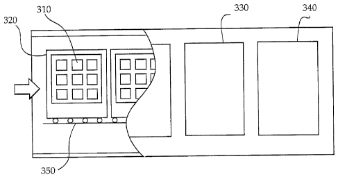
[0019] Figure 3 shows a plurality of work piece substrates on a device capable
of affixing
the substrates onto a carrier, that also has means that allow the pieces to be
advanced in a
precise fashion through the production apparatus.
[0020] Figure 4 shows a schematic of the pallet used in the present invention
populated
with a plurality of substrate work pieces.
[0021] Figure 5A shows an embodiment of the processing method wherein two
substrates
are fed and processed simultaneously by a sequential sputter-evaporate process
in accordance
with the present invention.
[0022] Figure 5B shows a top view of an embodiment of the processing method
wherein
two substrates are fed and processed simultaneously by a sequential sputter-
evaporate/sputter-
evaporate process.
[0023] Figure 6 illustrates another embodiment of the process in accordance
with the
invention wherein zones fiuther comprise one or more sub-zones.
DETAILED DESCRIPTION OF THE INVENTION
General Photovoltaic Stack Designs
-5-
CA 02586970 2007-05-09
WO 2006/053219 PCT/US2005/040933
[0024] The present invention employs a new production apparatus to produce
photovoltaic
devices. Of course, the particular apparatus will depend upon the specific
photovoltaic device
design, which can be varied.
[0025] Viewing FIG. 1, all layers are deposited on a substrate 105 which may
comprise one
of a plurality of functional materials, for example, glass, metal, ceramic, or
plastic. Deposited
directly on the substrate 105 is a barrier layer 110. The barrier layer 110
comprises a thin
conductor or very thin insulating material and serves to block the out
diffusion of undesirable
elements or compounds from the substrate to the rest of the cell. This barrier
layer 110 may
comprise chromium, titanium, silicon oxide, titanium nitride and related
materials that have the
requisite conductivity and durability. The next deposited layer is the back
contact layer 120
comprising non-reactive metals such as molybdenum. The next layer is deposited
upon the
back contact layer 120 and is a p-type semiconductor layer 130 to improve
adhesion between
an absorber layer 155 and the back contact 120. The p-type semiconductor layer
130 may be a
I-IIIa,b-VI isotype semiconductor, but the preferred composition is Cu:Ga:Se;
Cu:Al:Se or
Cu:In:Se alloyed with either of the previous compounds.
[0026] In this embodiment, the formation of a p-type absorber layer involves
the
interdiffusion of a number of discrete layers. Ultimately, as seen in FIG. 1,
the the p-type
semiconductor layers 130 and 150 combine into a single composite layer 155
which serves as
the prime absorber of solar energy. In this embodiment, alkali materials 140
are added for the
purpose of seeding the growth of subsequent layers as well as increasing the
carrier
concentration and grain size of the absorber layer 155, thereby increasing the
conversion
efficiency of the solar cell. Once deposited, the layers are thermally treated
at a temperature of
about 400 C - 600 C.
100271 After the thermal treatment, the photovoltaic production process is
continued by the
-6-
CA 02586970 2007-05-09
WO 2006/053219 PCT/US2005/040933
deposition of an n-type junction buffer layer 160. This layer 160 will
ultimately interact with
the absorber layer 155 to form the necessary p-n junction 165. A transparent
intrinsic oxide
layer 170 is deposited next to serve as a hetero-junction with the CIGS
absorber. Finally, a
conducting transparent oxide layer 180 is deposited to function as the top of
the electrode of the
cell. This final layer is conductive and may carry current to a grid carrier
that allows the
current generated to be carried away.
General Apparatus Configurations
[0028] A first embodiment of the invention is an apparatus for manufacturing a
photovoltaic
device comprising a means for providing a means for presenting the work pieces
to the
production apparatus where the orientation of the work pieces is vertical.
This vertical
orientation of the production train allows the work pieces to be disposed on
the front and back
of the product train and allows an increase in the capacity of the
manufacturing apparatus.
Surprisingly it has been found that provided the work piece substrates on a
vertical axis can be
accomplished by employing several factors which include:
= Limited substrate height so that reaction chamber technology can be
optimized
= Adequately isolation of each deposition or reaction chamber from the next
= Adequate monitoring and control of the reaction materials and deposition
sources
= Precise temperature control
[0029] It has been found, however, that a system needs a vertical substrate
which may
employ the positioning of target substrates on both sides of the vertical
plane so that a two fold
instance in production can be achieved and better and more economical use of
the reaction
parameters which are so assiduously controlled which involve relatively low
pressures and
higher temperatures can be more economically achieved.
-7-
CA 02586970 2007-05-09
WO 2006/053219 PCT/US2005/040933
[0030] A plurality of pallets holding multiple substrate pieces may be
employed as the
means for holding the substrates as the production train, in sequence, is
transported through the
plurality of reaction zones. These reaction zones include at least a zone
capable of providing an
environment for deposition of a semiconductor layer, and a zone capable of
providing an
environment for depositing precursor materials to form a p-type absorber
layer.
[0031] FIG. 4 shows a schematic view of a pallet. The pallet provides a
holding basis 400
for a plurality of small PV workpiece substrates 410, or working substrates
fixedly attached to
the pallet in a pre-determined manner so that the individual work pieces are
presented in each
treatment chamber in a precise and controllable fashion. The pallet itself is
engineered so that
the position of the pallet can be precisely determined. The pallet also has a
means 420 for
allowing attachment to a drive means to advance the pallet through the
treatment chamber.
Materials of the body of the pallet are chosen so that they are thermally
stable and do not
interact with the treatment or deposition materials used in the reaction or
deposition chamber.
[0032] Furthermore, the means for securing the work pieces to the pallet are
releasable. In
some instances the means for affixing the work piece is magnetic, either
because the substrate
of the workpiece is itself ferro-magnetic, or with an overlay that hold the
individual pieces to
the body of the pallet.
[0033] In a preferred einbodiment, the process may fuxther comprise a
substrate that runs
back-to-back with the substrate. In this embodiment substrates and are
oriented vertically in a
back-to-back configuration and run through zones performing identical process
operations.
[0034] FIG. 5A shows a top illustration of a portion of a reactor 500
processing substrates
501 and 502 in a back-to-back fashion and also illustrates a sequential
sputter-evaporate
process isolated by zone 511. To achieve back-to-back processing, heat sources
503 for
substrate 501 are mirrored as heat sources 507 for substrate 502. Likewise,
sputtering source
-8-
CA 02586970 2007-05-09
WO 2006/053219 PCT/US2005/040933
504, heat sources 505, and evaporative sources 506 for substrate 501 are
mirrored for substrate
502 as sputtering source 508, heat sources 509, and evaporative sources 510.
FIG. 5A shows
this vertical two sided manufacturing process at the top where the two
substrates in which the
photo devices are being made. Substrates 501 and 502 are processed from left
to right through
the heating, sputtering and evaporation chambers of a device forming layers to
thin films of the
PV device. The substrate is passed by sequential heaters 503 and 507 then
exposed to
sputtering target 503 and 509 with an atmosphere of le-3-le-2 torr. The
substrates are then
transported through differential pumping chamber at 1 e-7-1 e-6 torr and then
presented to an
evaporation deposition chamber where heaters 505 and 509 are used to heat each
of the
respective substrate 501 and 502 and evaporation sources of gases are provided
506 and 510
respectively.
[0035] FIG. 5B shows a top illustration of a portion of a reactor 512
processing substrates
521 and 522 in a back-to-back fashion with a sequential sputter-evaporate/
sputter-evaporate
process. As in FIG, 5A, sputter sources 534 for substrate 521 are mirrored as
sputter sources
528 for substrate 522. Likewise, heat sources 523 and 526, evaporative sources
524 and 527,
and sputtering source 525 for substrate 521 are mirrored for substrate 522 as
heat sources 529
and 532, evaporative sources 530 and 533, and sputtering source 531. Hence,
with the simple
duplication of heat and material sources, solar cell production may be
effectively doubled
within the same machine.
Alternative Pallet Based Manufacturing Schemes
[0036] FIG. 2 schematically represents a reactor 200 for forming solar cells.
A substrate
205 is fed left to right through the reactor. The reactor 200 includes one or
more processing
zones. referred to in FIG. 2 as 220, 230, 240 and 250, wherein each processing
zone comprises
-9-
CA 02586970 2007-05-09
WO 2006/053219 PCT/US2005/040933
an environment for depositing materials on a substrate 205. The zones are
mechanically or
operatively linked together within the reactor 200. As used herein, the term
environment refers
to a profile of conditions for depositing or reacting a material layer or
mixture of materials on
the substrate 205 while the substrate 205 is in a particular zone.
[0037] Each zone is configured according to which layer of the solar cell is
being processed.
For example, a zone may be configured to perform a sputtering operation,
including heat
sources and one or more source targets.
[0038] Preferably, an elongated substrate 205 is passed through the various
processing
zones at a controllable rate. It is further contemplated that the substrate
205 may have a
translational speed of .5 m/min to about 2 m/min. Accordingly, the process
internal to each of
the zones is preferably tuned to form the desired cross-section given the
residence time the
material is proximate to a particular source material, given the desired
transport speed. Thus,
the characteristics of each process, such as material and process choice,
temperature, pressure,
or sputtering delivery rate, etc., may be chosen to insure that constituent
materials are properly
delivered given the stack's residence time as determined by the transport or
translation speed.
[0039] According to the invention, the substrate 205 may be transported
through the process
in a vertically oriented palletized fashion in a "picture frame" type mount
for indexing and
transportation through the process, the latter of which is illustrated in FIG.
3. Referring to FIG.
3 one substrate or group of substrates 310 are mounted on a pallet 320 that
translates through
one or more zones 330 and 340 on track 350. In alternate embodiments the
process may further
comprise a second substrate or set of substrates placed in a back to back
configuration with
substrate 310.
[0040] It is contemplated that the background pressure within the various
zones will range
from 10-6 torr to 10-3 torr. Pressures above base-vacuum (10-6 torr) may be
achieved by the
-10-
CA 02586970 2007-05-09
WO 2006/053219 PCT/US2005/040933
addition of a pure gas such as Argon, Nitrogen or Oxygen. Preferably, the rate
R is constant
resulting in the substrate 205 passing through the reactor 200 from entrance
201 to exit 202
without stopping. It will be appreciated by those of ordinary skill in the art
that a solar cell
stack may thus be formed in a continuous fashion on the substrate 205, without
the need for the
substrate 205 to ever stop within the reactor 200.
[0041] The reactor in FIG. 2 may further comprise vacuum isolation sub-zones
or slit
valves configured to isolate adjacent process zones. The vacuum isolation sub-
zones or slit
valves are provided to facilitate the continuous transport of the substrate
between different
pressure environments.
[0042] The reactor shown in FIG. 2 is a plurality of N-processing zones 220,
230, 240 and
250. However, it should be recognized by one skilled in the art that the
reactor may comprise
zones 220, 230, 240, 250...N zones. The load/unload zones 210/211 comprise
zones that can be
isolated from the rest of the reactor and can be open to atmosphere.
[0043] In a preferred embodiment, the process may further comprise a substrate
206 that
runs back-to-back with substrate 205. In this embodiment substrates 206 and
205 are oriented
vertically in a back-to-back configuration and run through zones 220, 230,
240, and 250
performing identical process operations 222/221, 232/231, 242/241 and 252/251.
SPECIFIC PROCESSING STEPS
[0044] Of course, the method steps for producing a particular PV article
depends upon the
specific design of that article. CIS based PVs will have a different
production method than Si
based systems. The present invention is not so limited to one PV type and in
general any PV
could be made with the technology of the invention.
[0045] In cases of CIGS, the specific steps might include: loading a substrate
through an
-11-
CA 02586970 2007-05-09
WO 2006/053219 PCT/US2005/040933
isolated loading zone or like unit 210. In various embodiments, the isolation
zone 210 is
contained within the reactor 200. Alternatively, the isolation zone 210 may be
attached to the
outer portion of the reactor 200. The first processing zone 210 may further
comprise a
substrate preparation environment to remove any residual imperfections at the
atomic level of
the surface. The substrate preparation may include: ion beam, deposition,
heating, or sputter-
etch. These methods are known in the art and will not be discussed further.
[0046] A second processing zone may be environment for depositing a barrier
layer for
substrate impurity isolation, wherein the barrier layer provides an
electrically conductive path
between the substrate and subsequent layers. In a preferred embodiment, the
barrier layer
comprises an element such as chromium or titanium delivered by a sputtering
process.
Preferably, the environment comprises a pressure in the range of about 10-3
torr to about 10-2
torr at ambient temperature.
[0047] A third processing zone downstream from the previous zones comprises an
environment for the deposition of a metallic layer to serve as a back contact
layer. The back
contact layer comprises a thickness that provides a conductive path for
electrical current. In
addition, the back contact layer serves as the first conducting layer of the
solar cell stack. The
layer may further serve to prevent the diffusion of chemical compounds such as
impurities from
the substrate to the remainder of the solar cell structure or as a thermal
expansion buffer
between the substrate layer and. the remainder of the solar cell structure.
Preferably, the back
contact layer comprises molybdenum, however, the back contact layer may
comprise other
conductive metals such as aluminum, copper or silver.
[0048] A fourth zone provides an environment for deposition of a p-type
semiconductor
layer. As used herein, the p-type semiconductor layer may serve as an
epitaxial template for
absorber arowth. Preferably, the p-type semiconductor layer is an isotype I-
IIIVI2 material,
-12-
CA 02586970 2007-05-09
WO 2006/053219 PCT/US2005/040933
wherein the optical band gap of this material is higher than the average
optical band gap of the
p-type absorber layer. For example, a semiconductor layer may comprise
Cu:Ga:Se; Cu:AI:Se
or alloys of Cu:In:Se with either of the previous compounds. Preferably, the
materials are
delivered by a sputtering process at a background pressure of 10-6 to 10'2
torr and at
temperatures ranging from ambient up to about 300 C. Preferably, temperatures
range from
ambient to about 200 C.
[0049] A fifth zone, downstream from the previous zones, provides an
environment for the
deposition of alkali materials to enhance the growth and the electrical
performance of a p-type
absorber. Preferably, the alkali materials are sputtered, at ambient
temperature and a pressure
range of about 10-6 torr to 10"2 torr. Preferably, the material comprises NaF,
Na2Se, Na2S or
KCl or like compounds wherein the thickness ranges from about 150 nm to about
500 nm.
[0050] A sixth zone, also downstream from the previous zones, may comprise an
environment for the deposition of additional semiconductor layers comprising
precursor
materials for the p-type absorber layer. In a preferred embodiment, the sixth
zone may further
comprise one or more sub-zones for the deposition of the precursor layers. In
one embodiment,
the layer is formed by first delivering precursor materials in one or more
contiguous sub-zones,
then reacting the precursor materials into the final p-type absorber in a
downstream thennal
treatment zone. Thus, especially for CIGS Systems, there may be two material
deposition steps
and a third thermal treatment step in the format of the layer.
[0051] In the precursor delivery zones, the layer of precursor materials is
deposited in a
wide variety of ways, including evaporation, sputtering, and chemical vapor
deposition or
combinations thereof Preferably, the precursor material may be delivered at
temperatures
ranging from about 200 C - 300 C. It is desired that the precursor materials
react to form
the final p-type absorber as rapidly as possible. As previously discussed, to
this end, the
- 13 -
CA 02586970 2007-05-09
WO 2006/053219 PCT/US2005/040933
precursor layer or layers may be formed as a mixture or a series of thin
layers.
[0052] A manufacturing device may also have seventh processing zone downstream
from
previous processing zones for the thermal treatment of one or more of the
previous layers. The
term multinaries includes binaries, temaries, and the like. Preferably,
thermal treatment reacts
previously unreacted elements or multinaries. For example, in one embodiment
it is preferred
to have Cu, In, Se, and Ga in various combinations and ratios of multinary
compounds of
elements as the source for deposition on the work piece. The reactive
environment includes
selenium and sulfur in varying proportions and ranges in temperature from
about 400 C to
about 600 C with or without a background inert gas environment. In various
embodiments,
processing time may be minimized to one minute or less by optimizing mixing of
the
precursors. Optimal pressures within the environment depend on whether the
environment is
reactive or inert. According to the invention, within the thermal treatment
zone, the pressures
range from about 10-6 to about 10-2 torr. However, it should be noted that
these ranges depend
very much on the reactor design for the stage, the designer of the
photovoltaic device and the
operational variables of the apparatus as a whole.
[0053] The reactor may have an eighth processing zone for the formation of an
n-type
semiconductor layer or junction partner. The junction layer is selected from
the family II-VI, or
IIIx VI. For example, the junction layer may comprise ZnO, ZnSe, ZnS, In, Se
or InNS
deposited by evaporation, sublimation or chemical vapor deposition
methodologies. The
temperatures range from about 200 C to about 400 C.
[0054] Additionally, the process may also have a ninth zone having an
environment for
deposition of an intrinsic layer of a transparent oxide, for example ZnO.
According to the
invention, the intrinsic transparent oxide layer may be deposited by a variety
of methods
includin2 for example, RF sputtering, CVD or MOCVD.
-14-
CA 02586970 2007-05-09
WO 2006/053219 PCT/US2005/040933
[0055] In various embodiments, the process further has a tenth zone with an
environment
for the deposition of a transparent conductive oxide layer to serve as the top
electrode for the
solar cell. In one embodiment for example, aluminuin doped ZnO is sputter
deposited.
Preferably, the environment comprises a temperature of about 200 C and a
pressure of about 5
millitorr. Alternatively, ITO (Indium Tin Oxide) or similar may be used.
[0056] In one embodiment, as described above, the reactor may comprise
discrete zones
wherein each zone corresponds to one layer of photovoltaic device formation.
In a preferred
embodiment however, zones comprising similar constituents and or environment
conditions may
be combined thereby reducing the total number of zones in the reactor.
[0057] For example, in FIG. 6, zone 610 comprises sub-zones 611 and 612, zone
615
comprises sub-zones 616 and 617, and zone 620 comprises one zone, wherein each
zone and
sub-zone comprises a predetermined environment. In this example, a material A
may be
deposited in sub-zone 611 and a different material B may be deposited in sub-
zone 612,
wherein the environment of sub-zone 612 downstream from material A differs
from the
environment in sub-zone 611. Thus, the substrate 605 may be subjected to a
different
temperature or other process profiles while in different regions of the same
zone 610.
According to this embodiment, the zone may be defined as having a
predetermined pressure,
and a zone may include one or more regions, sub-zones, or phases therein, with
each sub-zone
configured to deposit or react a desired material or materials within the same
pressure
environment.
[0058] The substrate 605 may then be passed to chamber 615, where material C
is deposited
within sub-zone 616, and material D is deposited in sub-zone 617. Finally, the
substrate 605
reaches a zone 620, where a single material E is deposited.
100591 As will be annreciated by those of ordinary skill in. the art, the
reactor 600 may be
-15-
CA 02586970 2007-05-09
WO 2006/053219 PCT/US2005/040933
described as having a series of zones disposed between the entrance and exit
of the reactor along
a path defined by the translation of the substrate. Within each zone, one or
more constituent
environments or sub-zones may be provided to deposit or react a selected
target material or
materials, resulting in a continuous process for forming a solar cell stack.
Once the substrate
enters the reactor, the various layers of a solar stack are deposited and
formed in a sequential
fashion, with each downstream process in succession contributing to the
formation of the solar
cell stack until a finished thin film solar cell is presented at the exit of
the reactor.
[0060] While the present technique has been couched in terms of CIGS based
photovoltaic
stack designs it must be understood that the technique may also be employed
for the production
of other photovoltaic designs including production of silicon based systems
such as those
discussed in state of the art. For instance, it would be possible to use to
include carbon or
germanium atoms in hydrogenated amorphous silicon alloys in order to adjust
their optical
bandgap. For example, carbon has a larger bandgap than silicon and thus
inclusion of carbon in
a hydrogenated amorphous silicon alloy increases the alloy's bandgap.
Conversely, germanium
has a smaller bandgap than silicon and thus inclusion of germanium in a
hydrogenated
amorphous silicon alloy decreases the alloy's bandgap.
[0061] Similarly one could incorporate boron or phosphorus atoms in
hydrogenated
amorphous silicon alloys in order to adjust their conductive properties.
Including boron in a
hydrogenated amorphous silicon alloy creates a positively doped conductive
region.
Conversely, including phosphorus in a hydrogenated amorphous silicon alloy
creates a
negatively doped conductive region.
[0062] Hydrogenated amorphous silicon alloy films are prepared by deposition
in a
deposition chamber. Heretofore, in preparing hydrogenated amorphous silicon
alloys by
deposition in a deposition chamber, carbon, germanium, boron or phosphorus
have been
-16-
CA 02586970 2007-05-09
WO 2006/053219 PCT/US2005/040933
incorporated into the alloys by including in the deposition gas mixture
carbon, germanium,
boron or phosphorus containing gases such as methane (CH4), germane (GeH4),
germanium
tetrafluoride (GeF4), higher order germanes such as digermane (Ge2 H6),
diborane (B2 H6) or
phosphine (PH3). See for example, U.S. Patent. Nos. 4,491,626, 4,142,195,
4,363,828,
4,504,518, 4,344,984, 4,435,445, and 4,394, 400. A drawback of this practice,
however, is that
the way in which the carbon, germanium, boron or phosphorus atoms are
incorporated into the
hydrogenated amorphous silicon alloy is not controlled. That is, these
elements are
incorporated into the resulting alloy in a highly random manner thereby
increasing the
likelihood of undesirable chemical bonds.
100631 Thus, in cases where PV devices are manufactured, and specific and
controlled
reaction and or deposition conditions are required to produce the films of the
PV, the present
invention technology will be useful.
-17-