Note: Descriptions are shown in the official language in which they were submitted.
CA 02587367 2007-05-10
WO 2006/051516 PCT/IE2005/000127
Devices, Methods and Systems for Driving Displays
The present invention relates to devices, methods and
systems for driving displays and display elements, in
particular for driving electrochromic displays. A
typical electrochromic display comprises a glass
display screen, a substrate, tracks and electrochromic
segments or pixels, which change colour upon
application of an electrical potential.
In one embodiment, an electrochromic pixel comprises a
first electrode made of nanostructured films of
semiconducting metal oxides with a self-assembled
monolayer of electrochromic viologen molecules. The
charge to colour the electrochromic molecules is
supplied by a second nanostructured counter electrode,
comprised of a doped semiconductor. Between the
electrodes there is a reflector made of a porous film
of Titanium Dioxide.
Electrochromic displays are typically dc driven
devices. A voltage can be applied to each individual
segment or pixel of the display via a transparent
conductive track leading to the pixel from the edge of
the glass screen. The transparent conductive tracks are
usually fabricated from Indium Tin-Oxide and as such
behave in a manner similar to that of a resistor in
series with the pixel.
The electrochromic pixel has similar characteristics to
that of a capacitor in that it has the ability to store
CA 02587367 2007-05-10
WO 2006/051516 PCT/IE2005/000127
2
charge. The pixel is turned on or charged by applying a
voltage to its anode. The charge capacity of a pixel is
proportional to the area of the pixel. Once charged,
the pixel can be left in an open circuit configuration
and remains on. This characteristic of the
electrochromic display is called bistability. Like a
capacitor, however, the charge will slowly dissipate
after time, resulting in deterioration of the pixel
colouration.
This capacitor-resistor arrangement governs the rate at
which the pixel can be charged according to the
relationship dV/dt = V/RC. Thus the rate at which
individual pixels turn on is inversely proportional to
the area of the pixel and the resistance of the
associated track. As such, individual pixels may charge
at different rates. Pixels, like capacitors, can be
damaged when exposed to applied voltages exceeding
their capacity. Thus, due to this limitation on the
applied voltage, and large ITO track resistances
combined with large capacitances, the response time to
the switching of electrochromic displays can be quite
slow.
Exposure to W light and voltage coupling from
neighbouring pixels being switched on results in
potentially dangerous variations within the individual
pixels. As such, the pixels can reach their voltage
capacity while still being driven, resulting in damage
to the pixels
CA 02587367 2007-05-10
WO 2006/051516 PCT/IE2005/000127
3
US 5,973,819 discloses a driver for controlling the
charge state (i.e., colour level) of an electrochromic
device. After initiation the driver iteratively
modifies and measures a charge level of the
electrochromic device until a maximal or minimal charge
level is achieved.
In particular, US 5,973,819 discloses connecting a
single driver element through a switching matrix to
each of a number of electrochromic (EC) elements in
turn.
According to the present invention there is provided a
device for driving a multi-cell display according to
claim 1.
Using the present invention, the state of an EC element
can be sensed while the remaining cells are driven, so
providing more control of a display.
In preferred embodiments, potentially dangerous
variations within the pixels, caused by photoelectric
effect, voltage coupling from other pixels being turned
on or the like, can be sensed and compensated for. The
response time of the pixels is improved by using higher
driving voltages in a safe controlled environment. Once
charged the pixel can be left in an open-circuit state
ensuring improved lifetime for the pixels. Leakage
current from and between the pixels can be detected
CA 02587367 2007-05-10
WO 2006/051516 PCT/IE2005/000127
4
using voltage sensing and measures can be taken to
maintain the correct appearance of the display.
In a further aspect, a method and system for driving a
display element is presented in which a varying drive
signal is applied to the display element to increase
the charge transfer over what would occur using a
constant drive signal. In one embodiment a sawtooth
waveform can be used to drive the display element and
achieve an approximately constant current
charging/discharging of the display element. The method
and system can be applied to a variety of display
elements including electrochromic display elements
which can exhibit differences in coloration between an
edge portion and a center portion. In one embodiment
the voltage at the edge portion is monitored and use of
a sawtooth waveform allows for propagation of charge
across the display element and a more accurate
measurement of the state of charging at the edge
portion.
Embodiments of the invention will now be described, by
way of example, with reference to the accompanying
drawings, in which:
Fig. 1 is a system diagram of a device of the present
invention connected to a micro-control unit and an
electrochromic display;
Fig. 2 illustrates a block diagram of the device of
Fig. 1 according to the present invention;
CA 02587367 2007-05-10
WO 2006/051516 PCT/IE2005/000127
Fig. 3(a) is a timing diagram of the device of Fig. 1
operating in programming mode;
5 Fig. 3(b) is a timing diagram of the device of Fig. 1
operating in sense mode;
Fig. 4 is a plot of an applied pixel voltage against
time;
Fig.5 is a plot of an applied pixel voltage against
time including sensing incidents;
Fig. 6 illustrates a display containing segments, with
the segments having an edge portion and a center
portion;
Fig. 7 illustrates a model for an electrochromic
display element;
Fig. 8 illustrates a drive signal for an electrochromic
display element;
Fig. 9 illustrates a block diagram for a display
element driver; and
Fig. 10 illustrates an embodiment of a wave shaping
circuit.
Referring now to Fig. 1 of the accompanying drawings, a
system diagram of a device for driving a multi-cell
CA 02587367 2007-05-10
WO 2006/051516 PCT/IE2005/000127
6
display is indicated, generally at 10, connected to a
micro control unit 12 and an electrochromic display 14.
The nanostructured film electrode of the electrochromic
display pixel comprises an enormous surface area with a
high number of electrochromic viologen molecules bound
to the surface, enabling the viologens to be switched
from colourless to coloured and vice versa very
quickly. The high number of viologen molecules attached
gives strong colouration and the high speed of electron
transfer gives high switching speeds. Different colours
can be achieved through using different viologen
molecules. The doped semiconductor electrode can store
charge due to its high capacitance and as such the
display device is endowed with a memory, resulting in
bistability and low power consumption.
According to the preferred embodiment of the invention,
the device 10 comprises 65 output channels 16, labelled
as 0[11, O[2] ,...0[641, 0[651. Each output channel 16 is
connected via a corresponding transparent conductive
track 18 to a cathode 20 of one of 65 segments or
pixels 22 of the electrochromic display 14. It will be
appreciated that fewer than the 65 pixels may be used.
Likewise, more than 65 pixels can be used by joining or
cascading a number of ICs together.
In one embodiment, the pixels 22 can be turned on or
off by application of a dc voltage to the cathodes 20.
A common anode 24, corresponding to the cathodes 20 is
connected to a supply voltage Vcc.
CA 02587367 2007-05-10
WO 2006/051516 PCT/IE2005/000127
7
In one embodiment, by connecting the anode to a
positive voltage relative to ground, the requirement of
a negative pixel voltage can be avoided. When the pixel
is on, the pixel voltage applied to the cathode 20 is
positive but lower than Vcc.
The output channels 16 have been designed as voltage
sources that source and sink current in order to get
the connected pixel 22 to the applied voltage as
quickly as possible. The 65 output channels 16 each
support 4 voltage states; two 'on' voltage states,
Vrefl and Vref2, an open circuit or high impedance (Hi-
Z) state and an 'off' voltage state.
The two 'on' voltages are defined by the voltages at
pins Vrefl and Vref2, located on the device 10. An
internal circuit and an external current reference
resistor R3 define a constant current source that sinks
through Vref2 allowing a pair of resistors, Rl and R2,
to be used to accurately define the voltages at Vrefl
and Vref2. The voltage drop at Vrefl and Vref2 will
remain constant relative to Vcc as they will always
have a constant current flowing through them, ensuring
that the contrast of the electrochromic display 14 will
not change if the supply voltage Vcc varies.
The constant current is defined by the value of the
resistor R3, connected between ground and an Iref pin
located on the device 10. In this embodiment, the
equation for the constant current is 1.25/R3. For
CA 02587367 2007-05-10
WO 2006/051516 PCT/IE2005/000127
8
example, if resistor R3 has a value of 270KS2, the
current flowing through resistors R1 and R2 will be
4.6 A. Similarly, if resistor R3 has a value of 888KSZ,
the current flowing through resistors Ri and R2 will be
1.43 A. The values of Rl and R2 are then set
accordingly to provide the required voltage drop from
Vcc to drive the display 14. In this embodiment, Vrefl
should be set to a value of 0.8V below Vcc and Vref2
should be set between 1.5V and 2V below Vcc.
The pixels 22 assume the open circuit or Hi-Z State
when the output channels 16 are disconnected from the
pixels 22. Once the 'turn on' voltage has been applied
to the pixels 22, the pixels can assume the Hi-Z state
without any change to the display image. This is due to
the ability of the pixels to store charge and is known
as bistability. The same display image will be
maintained for a period of time before the voltage
eventually changes due to charge leakage, causing the
pixel image to fade. Depending on the characteristics
of the pixel, the image could fade in a matter of
minutes or days.
The 'off' state is achieved by setting the state for
the output channel 16 to Vcc, thus eliminating the
voltage drop across the terminals of the pixel, and
causing the pixel to turn off. In general, once the
pixels reach a voltage of approximately 400mV or less,
they are assumed to be off. Once the pixel has turned
off, it should be set to the Hi-Z State.
CA 02587367 2007-05-10
WO 2006/051516 PCT/IE2005/000127
9
The device 10 further comprises three inputs, DATA IN,
SCLK and LOAD, which are connected to corresponding
outputs, 26, 28, and 30 respectively, located on the
micro control unit 12. An output, SENSE, provided on
the device 10 is connected to an Analogue-to-Digital
converter, A/D, located on the micro control unit 12.
The device 10 operates in one of two modes at any one
time, programming mode or sense mode. In order to
program the state of some or all of the pixels of the
display 14, the device needs to operate in the
programming mode. In programming mode, the device 10 is
provided with information representing the pixels at
its input DATA IN in accordance with the clock signal
provided to the input SCLK. The device 10 operates in
the sense mode to monitor the behaviour of each of the
pixels 22. In sense mode, a signal representing the
state of a pixel is provided at the SENSE output and
fed to the analog-to-digital converter A/D, where it is
compared with a reference value. This mode enables the
MCU 12 to sense variations in pixel voltage due to
exposure to W light, voltage coupling from
neighbouring pixels being switched on, irregularities
in the pixel, response to the applied voltage and other
varying factors.
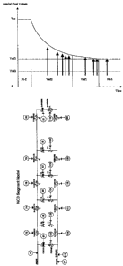
Referring now to Fig. 2 there is provided a block
diagram of the device 10, according to the preferred
embodiment of the invention.
CA 02587367 2007-05-10
WO 2006/051516 PCT/IE2005/000127
The device 10 comprises a control logic unit, 32 and a
130-bit shift register 34. The register 34 is connected
to a 130-bit latch 36. The content of the 130-bit latch
36 is fed to 65 2-to-4-bit decoders 38, the outputs of
5 which are connected to 65 corresponding CD
(chromodynamic, i.e. electrochromic) drivers 40. The
NCD drivers are in turn connected to the output
channels 16. The truth table for the operation of each
decoder 38 is depicted below as Table 1.
Inputs Charging
State
A B Indicator
0 0 Hi-Z
0 1 Vrefl
1 0 Vref2
1 1 Vcc
Table 1.
The 130-bit shift register 34 is also connected to a 7-
bit latch 44. The content of the 7-bit latch 44 is fed
to a 7-to-65-bit decoder 46. The outputs of the decoder
46 are connected to 65 respective switches 42, which
control the monitoring of the pixels. The 65 NCD
drivers 40 are connected to the 65 switches 42, which
in turn provide an input to the output SENSE.
CA 02587367 2007-05-10
WO 2006/051516 PCT/IE2005/000127
11
The input DATA IN is connected to the 130-bit shift
register and the inputs SCLK and LOAD are connected to
the control logic unit 32, which is in turn connected
to the 130-bit shift register 34 at two points. The
SCLK input is a clocked input and is controlled by the
MCU 12. In the preferred embodiment, the maximum
frequency of the SCLK is 10MHz. The LOAD input can
assume a high or low signal value and is also
controlled by the MCU 12. The value of the LOAD input
determines whether the shift register 34 is filled with
7-bits or 130-bits.
For the device 10 to operate in the programming mode,
the micro control unit must send a low signal value to
the control logic unit 32 via the device input LOAD as
illustrated in Fig. 3(a). The micro control unit 12
then feeds 130-bits into the register 34, via the input
DATA IN. Each 2-bit binary value of the 130 bits
represents the desired state of one of the 65 pixels.
Data, representing the desired state for each of the 65
pixels, is shifted from the DATA. IN input into the
register 34 at each low to high transition of the SCLK
clock. Once the shift register 34 is filled with 130-
bit binary values, the MCU 12 provides a high signal
value at the LOAD input, causing the content of the
shift register to be loaded into the 130-bit latch 36.
The decoders 38 decode the data, and supply the
corresponding NCD drivers 40 with the desired state
information for each pixel. The NCD drivers 40 provide
CA 02587367 2007-05-10
WO 2006/051516 PCT/IE2005/000127
12
the output channels 16 with the requested voltage,
according to Table 1, which is applied to the pixels.
When the device input LOAD is supplied with a high
signal value, the mode of operation changes from
programming mode to sense mode, as illustrated in Fig.
3(b). In sense mode, each bit of a 7-bit binary value
representing the pixel number to be sensed is loaded
into the shift register 34 on every low to high
transition of the SCLK clock. After 7 clocked shifts,
the LOAD input signal changes momentarily from high to
low before returning to the high state. This causes
the 7-bit binary value to be loaded into the 7-bit
latch 44, from where it is decoded by the decoder 46
and applied to one of the 65 switches 42 corresponding
to the pixel number. This switch 42 disconnects the
corresponding NCD driver 40 from the corresponding
output channel 16. This causes the pixel 22 to assume
the Hi-Z state enabling its voltage to be sensed. The
sensed voltage is applied to the SENSE output and fed
to the Analogue-to-Digital Converter A/D located on the
micro control unit. The A/D converts the signal to a
digital value, which is compared with a fixed reference
value, the outcome of which determines whether it is
required to change the state of the pixel 22. When
sensing is finished, the NCD driver 40 is reconnected
to its associated output channel 16.
Referring now to Fig. 4 there is illustrated a plot of
the applied pixel voltage against time. In order to
accelerate switching and increase the responsiveness of
CA 02587367 2007-05-10
WO 2006/051516 PCT/IE2005/000127
13
the display 12, the required pixels are driven by a
voltage Vref2, which exceeds the safe voltage limit of
the pixels. Ideally, before the pixels become fully
charged, the safe voltage Vrefl is applied to ensure
that the pixels don't exceed their voltage capacity for
too long.
In a first embodiment, as depicted in Fig. 5, the
device 10 will operate in the sense mode during
charging until it is sensed that a pixel voltage is
within a predefined range of a fixed reference voltage
or Vrefl, and that the applied voltage thus needs to be
changed from Vref2 to Vrefl to avoid overcharging. It
will be appreciated however, that the sense mode can
also be used to determine whether a pixel voltage in
the Hi-Z state has drifted and thus requires a voltage,
Vrefl or Vref2, to be applied to return the pixel
voltage to the desired level. The MCU 10 will then send
a low signal to the LOAD input causing the device 10 to
change to programming mode and the required voltage
(including open circuiting) will be applied to the
associated pixel output channel 16 by setting the input
bits for the pixel to the required state. The device 10
will then return to sense mode.
In another embodiment, the MCU 12 contains timing
information relating to each individual pixel of the
display 12. This timing information is derived from the
known capacitance of each pixel and the resistance of
its associated ITO track and provides the MCU 12 with
an estimated time period for the application of both
CA 02587367 2007-05-10
WO 2006/051516 PCT/IE2005/000127
14
Vrefl and Vref2. In this embodiment, the MCU 12 timing
information also contains an estimated time for which
the display 14 will remain coloured. This timing
information is used to schedule the sensing of the
pixels. If a pixel is sensed according to the schedule,
and it is determined that due to voltage variations, it
has not reached the predefined range which defines the
necessity to change the applied voltage, the timing
information associated with that pixel voltage is
incremented by a predefined amount, and the schedule is
updated accordingly. Similarly, if a pixel is sensed
according to the schedule, and it is determined that
due to voltage variations, it has passed the predefined
range which defines the necessity to change the applied
voltage, the timing information associated with that
pixel voltage is decremented by a predefined amount,
the schedule is updated accordingly and the required
voltage (including open circuiting) is applied to the
pixel. Likewise, if the MCU 12 detects that a pixel in
the Hi-Z state has leaked charge, it will adjust the
related timing information, update the schedule and
change the mode of operation of the device 10 to
programming mode in order to apply the required safe
voltage to 'top up' the pixel.
In the preferred embodiment, the device 10 will operate
in programming mode in order to change the applied
voltage of one or more of the pixels in accordance with
both the estimated timing information stored in the MCU
12 and the outcome of the sensing operation.
CA 02587367 2007-05-10
WO 2006/051516 PCT/IE2005/000127
In another embodiment, the timing information is
incremented or decremented by an amount directly
related to the approximate rate of charge of the pixel
at the time the pixel is sensed. In order to determine
5 the rate of charge of a pixel, the MCU 12 stores the
time at which each pixel enters each state.
In another embodiment, when the sensing function is
carried out on a pixel, the MCU determines the time and
10 associated voltage of the pixel. The same pixel is
sensed again, and again the MCU determines the time and
associated voltage of the pixel. The MCU can then use
these two results to determine the rate of charge of
the pixel and update the timing information as
15 appropriate.
In another embodiment, each time the sensing function
is used, the MCU determines a first time and associated
voltage of the pixel, then momentarily reconnects the
pixel output channel to its NCD driver before
determining a second time and associated voltage for
the pixel. These values are then used to determine the
rate of charge of the pixel and update the timing
information as appropriate.
In an alternative embodiment, the Analogue-to-Digital
Converter located on the MCU 12 is replaced with a
comparator, which compares the sensed voltage signal
with the safe voltage Vrefl.
CA 02587367 2007-05-10
WO 2006/051516 PCT/IE2005/000127
16
In the preferred embodiment, the device can be set to a
standby state. This is achieved by setting all of the
output channels to the Hi-Z state and setting the
device to programming mode. In this state, the constant
current source that provides the Vrefl and Vref2
voltages is shut down, enabling the device 10 to
achieve very low power consumption.
It will be appreciated that the timing information may
be derived from a number of factors such as the size of
the pixel, its proximity to a crossover point, the
conductivity of the substrate resistance, the context
within which it is switching or a combination thereof.
For example, if a pixel is the only one being turned on
when all the others are bleached (being turned off),
the effect of the bleaching pixels (turning off) will
be to 'push up' the apparent voltage of the substrate
to such a level that the pixel that is turning on will
colour quicker than if it was one of many pixels to be
turning on.
In particular, when implementing delayed sensing, the
pre-programming or currently calculated delay value
could be factored with a coefficient value that is
determined by the amount of active area turning off
compared with the amount of active area turning on at
that time.
For example, if a large aggregate area is being
switched off while a small area is being switched on, a
relatively large amount of charge may be freed up from
CA 02587367 2007-05-10
WO 2006/051516 PCT/IE2005/000127
17
the area being switched off. This charge may then be
available to colour the small area being switched on.
This large amount of excess charge is likely to result
in the small area being driven to the desired voltage
more quickly than normal, and if care is not exercised,
will result in the small area being overdriven.
Accordingly, if the driver would normally wait a delay
time tl before sensing if a given pixel, which is being
switched on, has reached the target voltage, this time
ti may be adjusted by a coefficient to reduce the time,
to take account of the charge available from the large
area being switched off.
The coefficient, which may usefully be calculated as a
function of the area being switched off and the area
being switched on, causes the pixel to be sensed
earlier than normal, in order to anticipate the
quicker-than-normal charging time and thereby sense the
pixel before it has been overdriven. Conversely, if a
large area is being switched on with only a small area
being switched off, the reduced charge availability on
the anode (or backplane) may result in the pixels
taking longer than normal to be fully charged, and this
can be compensated for by adjusting t1 upwards using a
coefficient greater than unity.
Precise details of how a coefficient will be calculated
will depend on the characteristics of the display and
driving circuitry, but at a first level of
CA 02587367 2007-05-10
WO 2006/051516 PCT/IE2005/000127
18
approximation the coefficient may be proportional to
[(area being switched on)/(area being switched off)].
Furthermore, because of the resistive nature of the
substrate, pixels close to the pixel that is turning on
will have more of an effect on the switching time of
that pixel than pixels that are further away, i.e. the
microcontroller would internally know the size and
position of each pixel. In each switch it may calculate
for every pixel a coefficient value based on an
equation that relates the transition of every other
pixel with the location of every other pixel.
Again due to the resistive nature of the substrate
after a switch, pixels can be at different contrasts
even though their sensed voltage is the same. This is
due to the local fluctuations in the apparent voltage
of the substrate. It is possible to compensate for
these different contrasts by setting different
threshold voltages for each turning-on pixel. These
threshold voltages may be calculated by the
microcontroller as a function of what has previously
been on and turned off, what was previously off and has
turned on and the locations of these pixels.
Figure 6 illustrates a 7 segment display which can be
realized using electrochromic elements such as those
described herein. As illustrated in Figure 6, the
segments can be considered to have an edge portion 60
and a center portion 61. In an alternate embodiment the
display elements are electrophoretic elements which
CA 02587367 2007-05-10
WO 2006/051516 PCT/IE2005/000127
19
serve as electronic ink. When used herein, the term
element refers generally to a display element, with
segments such as those shown in Figure 6 being one type
of display element. Other types of display elements of
different shapes and configurations, including
electrophoretic display elements, are understood to be
elements as well.
As illustrated in Figure 7, an electrochromic display
element can be modelled as a set of distributed
variable resistors and capacitors. The elements of the
model are made variable because their values change
over time based on the state of charge and discharge at
the various points in the electrochromic display
element. Referring again to Figure 7, anode 70
represents the anode of the electrochromic display
element along which are distributed anode resistances
72, 74, 76, 78, and 80. Vdrive 71 represents the
conducting element on which the drive signal is
applied. In one embodiment anode 70 is common to the
entire electrochromic display element with Vdrive 71
representing an individual electrode which addresses a
pixel or segment in the display. Vdrive 71 can be
modelled as having distributed drive track resistances
112, 114, 116, 118, 120, and 122.
The display elements illustrated in Figure 6 having an
edge portion 60 and a center portion 61, will, when
realized as electrochromic display elements, charge
differently at edge portion 60 than at center portion
61. Thus, the electrochromic display element has
CA 02587367 2007-05-10
WO 2006/051516 PCT/IE2005/000127
spatial varying properties as well as time varying
properties. The spatial variations can be modelled as
distributed variable capacitances and resistances which
appear between the anode 70 and Vdrive 71 and are shown
5 in figure 7 as edge capacitance 81 and edge resistance
100, to center capacitance 91 and center resistance
110, with intermediate capacitances 83, 85, 87 and 89,
in series with intermediate resistances 102, 104, 106,
and 108 respectively.
The electrochromic display element behaves more
similarly to a transmission line than to a lumped
resistance and capacitance. In addition to its
transmission line like properties, the fact that the
impedance at different points in the electrochromic
element will vary depending on its state of charge
causes the electrochromic display element to act as a
time varying transmission line. As a result, it can be
difficult to obtain uniform charging and coloration of
an electrochromic element. A time varying waveform can
be utilized to obtain uniform coloration by essentially
launches a wave into the element, with that waveform
being matched to the spatial and time varying impedance
of the electrochromic element.
Use of a modified (and potentially matched) waveform is
preferable over a constant waveform applied as a drive
signal, because the constant waveform drive signal can
cause the segment to color very quickly but not evenly.
By varying the drive signal to the display element over
time, increased charge transfer over which would be
CA 02587367 2007-05-10
WO 2006/051516 PCT/IE2005/000127
21
obtained using a constant drive signal can be obtained.
Additionally, varying the Vdrive waveform can prevent
unsafe charging of the display element. In one
embodiment the waveform is varied to achieve an
approximately constant current charging or discharging
of the electrochromic display element. Constant
current charging permits more uniform coloration of the
electrochromic display element than can be obtained
using a constant voltage drive signal with a charging
current that may initially be very large but which
decreases as the element charges.
Referring to figure 8, a sawtooth waveform can be used
to accomplish an approximately constant current drive
signal for the electrochromic display element. A
positive going sawtooth signal such as OFF 151 of
Figure 8 can be used to turn the electrochromic display
element off while a negative going signal such as ON
153 can be used to turn the electrochromic display
element on. In one embodiment, the drive signal is
varied from a voltage referred to as V-safe 160 to a
voltage of a higher magnitude such as V-attack 162. In
one embodiment V-attack 162 is equal to Vdrive-ON 154.
In one embodiment V-safe 160 is equal to Vrefl, which
has a value of approximately 500 mV. In this
embodiment V-attack 162 is equal to Vdrive-ON 154 which
has a value of approximately 1000 mV. A signal of a
similar magnitude but opposite polarity, such as OFF
151, can be used to turn the element off. In one
embodiment these signals are referenced to the level
established by a Virtual-GND 152. As illustrated in
CA 02587367 2007-05-10
WO 2006/051516 PCT/IE2005/000127
22
Figure 8, a rise time 163 and decay time 165 can be
associated with the sawtooth waveforms.
One of the advantages of using a sawtooth waveform is
that the decreasing edge of the sawtooth waveform can
be used to draw charge off of the edge portion 60 on
the display element thus creating more even charging
across the display element and resulting in more
uniform coloration. Another advantage of using the
sawtooth waveform illustrated in Figure 8 is that the
safe voltage for the electrochromic display element, in
this case V-safe 160, can be exceeded momentarily while
the drive signal is ramped up to V-attack 162, and then
ramped back down. Because of the transmission line
nature of the display element, ramping ON 153 up to
Vdrive-ON 162 does not result in the entire display
element reaching a voltage which is above the safe
voltage, but instead allows the charge to propagate
through the display element to achieve uniform
coloration.
In one embodiment the voltage at the edge portion 60 of
the display element is sensed to determine the state of
charge of the display element. This allows for
monitoring of the amount of charge placed on the
display element and ensures that the element is not
damaged. Because of the transmission line like nature
of the display element, the use of the variable
waveform not only allows for the charge to be
effectively propagated along the display element, but
also ensures that when the edge portion 60 is monitored
CA 02587367 2007-05-10
WO 2006/051516 PCT/IE2005/000127
23
it provides a voltage reading which is representative
of the average voltage and amount of charge on the
entire electrochromic element. By using a variable
waveform, such as the sawtooth waveform illustrated in
Figure 8, it becomes possible to allow charge to
propagate to the center portion 61 of the display
element while measuring a safe voltage at edge portion
60. Even though what appears to be a quote "unsafe"
voltage has been applied to the display element it
simply results in charge propagating to the center the
display element and does not result in an unsafe long-
term voltage being applied to the entire display
element.
Figure 9 illustrates a block diagram for one embodiment
of a driver system in which MCU 12 is used in
conjunction with digital-to-analogue converters (DACS)
170, voltage to constant current circuits 172, a wave
shaping circuit 174, a current control capacitor 182, a
phase reversal circuit 180, window comparator 176, a
virtual ground generator 178 (producing VIRTUAL-GROUND
152) and output channels 16. In one embodiment, MCU 12
is used to control DACS 170 to produce waveforms that
are used by voltage to constant current circuits 172
and window comparator 176, the outputs of both being
used to drive wave shaping circuit 174 which works in
conjunction with current control capacitor 182 to
produce waveforms which are inverted by phase reversal
circuit 180 and applied to the output channels 16 for
application to the electrochromic display 181.
CA 02587367 2007-05-10
WO 2006/051516 PCT/IE2005/000127
24
Figure 10 represents one embodiment of wave shaping
circuit 174. In this embodiment, a first current mirror
transistor Q6 190 is used in conjunction with a second
current mirror transistor Q16 192, with 190 and 192
forming a matched pair. The current in load 191 is set
using a preset resistance (not illustrated) and is
mirrored on the collector of current mirror transistor
Q6 190. This produces a constant current which is used
to charge current control capacitor 182 through Q9 199.
When the voltage on current control capacitor 182
reaches V-SAFE 160, comparator IC2A 197 switches Q13
200 off, Q9 199 on. Current control capacitor 182 now
discharges to V-ATTACK 162. Current control capacitor
182 is discharged by a constant current. When the
voltage on current control capacitor 182 discharges to
V-ATTACK 162, IC2A 197 switches Q13 200 off and Q9 199
on, and the cycle repeats.
The constant current applied to current control
capacitor 182 produces a linear voltage waveform (both
rise and decay) on current control capacitor 182, with
that signal being buffered by IC4C 206 and push-pull
transistor pair comprised of Q7 201 and Q12 202. The
resulting voltage, VDRIVE-ON 154 drives the segments,
and is inverted by IC4D 203, and transistors Q5 204 and
Q8 205 to produce VDRIVE-OFF 150. VDRIVE-OFF 150 is
used to drive the segments off.
Wave shaping circuit 174 can be used to vary the
parameters of rise time 163, decay time 165, V-SAFE
160, and V-ATTACK 162. By using a sharp rise time the
CA 02587367 2007-05-10
WO 2006/051516 PCT/IE2005/000127
segments can be colored from the edge portion 60 to the
center portion 61. A softer rise time produces a more
uniform fill and colors from the center portion 61 to
edge portion 60.
5
Using the drive waveforms described herein allows for
constant current charging of the display element, with
the ability to ramp the voltage down and avoid
misleading readings regarding the state of the charging
10 as detected by a voltage sensor located in edge portion
60. In one embodiment if the segment has not reached
the correct voltage with the applied charge (from the
applied waveform) an additional charge is provided.
When the segment has reached the correct voltage the
15 driver goes to a high impedance state.
In one embodiment the system shown in Figure 9 can be
used to learn the electrochromic display 181 so that it
can drive different sized segments by varying the
20 amount of charge applied to each segment. Since a
linear relationship exists between the voltages applied
to the current mirror transistors and the area
underneath the sawtooth voltage waveform, the sawtooth
voltage waveform can be modulated by MCU 12 on a
25 segment by segment basis.
The present invention is not limited to the embodiments
described herein, which may be amended or modified
without departing from the scope of the present
invention.