Note: Descriptions are shown in the official language in which they were submitted.
CA 02587674 2007-05-15
WO 2006/055736 PCT/US2005/041731
1
METHOD AND APPARATUS FOR READING CODED MICROBEADS
CROSS REFERENCES TO RELATED APPLICATIONS
This application claims benefit to U.S. provisional
patent application no. 60/628,897 (WFVA/CyVERA nos. 714-
1.9/CV 0056PR), filed November 16, 2004, which is hereby
incorporated by reference in their entirety.
The following cases contain subject matter also
related to that disclosed herein and are incorporated
herein by reference in their entirety, as follows: U.S.
Provisional Patent Application Serial No. 60/441,678,
filed January 22, 2003, entitled "Hybrid Random Bead/Chip
Microarray" (Attorney Docket No. CC-0574); U.S. Patent
Application Serial No. 10/645,689, filed August 20, 2003,
entitled "Diffraction Grating-Based Optical
Identification Element" (Attorney Docket No. CC-0648);
U.S. Patent Application Serial No. 10/645,686 filed
August 20, 2003, entitled "End Illuminated Bragg Grating
based Optical Identification Element" (Attorney Docket
No. CC-0649); U.S. Patent Application Serial No.
10/661,031, filed September 12, 2003, entitled "End
Illuminated Bragg Grating based Optical Identification
Element", (Attorney Docket No. CC-0649A); U.S. Patent
Application Serial No. 10/661,082, filed September 12,
2003, entitled "Method and Apparatus for Labeling Using
Diffraction Grating-based Encoded Optical Identification
CA 02587674 2007-05-15
WO 2006/055736 PCT/US2005/041731
2
Elements" (Attorney Docket No. CC-0650); U.S. Patent
Application Serial No. 10/661,115, filed September 12,
2003, entitled "Assay Stick" (Attorney Docket No. CC-
0651); U.S. Patent Application Serial No. 10/661,836,
filed September 12, 2003, entitled "Method and Apparatus
for Aligning Microbeads in order to Interrogate the Same"
(Attorney Docket No. CC-0652); U.S. Patent Application
Serial No. 10/661,254 filed September 12, 2003, entitled
"Chemical Synthesis Using Diffraction Grating-based
Encoded Optical Elements" (Attorney Docket No. CC-0653);
U.S. Patent Application Serial No. 10/661,116 filed
September 12, 2003, entitled "Method of Manufacturing of
a Diffraction grating-based identification Element"
(Attorney Docket No. CC-0654); U.S. Provisional Patent
Application Serial No. 60/519,932, filed November 14,
2003, entitled, "Diffraction Grating-Based Encoded
Microparticles for Multiplexed Experiments" (Attorney
Docket No. CC-0678); and U.S. Patent Application Serial
No. 10/763,995 filed January 22, 2004, entitled, "Hybrid
Random bead/chip based microarray" (Attorney Docket No.
CV-0054).
CA 02587674 2007-05-15
WO 2006/055736 PCT/US2005/041731
3
BACKGROUND OF THE INVENTION
1. Field Of Invention
The present invention relates to a method and
apparatus for reading a code on an optical element; and
more particularly, to a method and apparatus for reading
a code on a microbead that is typically 1-1000 microns in
size using a Fourier plane analysis technique.
2. Description of Related Art
Tiny microbeads that are individually identifiable
have many applications in drug discovery, genomics,
chemistry, and security. Microbeads are very small
objects, typically 1-1000 microns (um) in feature size.
They may be cylindrical, cubic, rectangular, or any other
shape. Typically microbeads are composed of silica based
glass. Coded microbeads are individually identifiable.
There are many methods available to encode microbeads.
Known methods for encoding microbeads include
fluorescence intensity and/or color, chemical techniques,
spatial marks on the particles and radio-frequency
encoding. However, the known ways involve using
expensive, high resolution, optical techniques for
imaging and reading the code off the microbead.
For example, Figure 1 shows such a spatial imaging
technique generally indicated as 10' for reading encoded
particles or microbeads that is known in the art, and
CA 02587674 2007-05-15
WO 2006/055736 PCT/US2005/041731
4
includes an input light source 12' for passing input
light through a microbead 14 and imaging optics,
including an imaging lens 16, to project an image of the
microbead 14 on an imaging plane 18 for reading the image
using expensive, high resolution, imaging equipment 20.
The imaging lens 16 is arranged between the microbead 14
and the image plane 18 at a distance of two focal lengths
from each. The imaging optics are also expensive to
provide the high resolution image needed to read or
interpret the code on the microbead.
In view of this, there is a need in the industry for
a less expensive way to encode and decode microbeads.
SUMMARY OF INVENTION
In its broadest sense, the present invention
provides a new and unique method and apparatus for
reading a microbead having a code thereon, wherein the
code is projected on and read from a Fourier plane.
In operation, the code is projected on the Fourier
plane by first scattering input light off (reflected or
transmitted) the microbead. The light scattered from the
microbead is directed through an optical arrangement
having a transform lens for projecting the code on the
Fourier plane, and read on the Fourier plane with a
Fourier plane reading device, including a charge coupled
device (CCD) or other suitable Fourier plane reading
CA 02587674 2007-05-15
WO 2006/055736 PCT/US2005/041731
device and a processor for performing Fourier plane
analysis. The transform lens is arranged between the
microbead and the Fourier plane at a distance of one
focal length from each, while the charge coupled device
(CCD) or other suitable Fourier plane reading device is
arranged on the Fourier plane. The whole thrust of the
present invention is to analyze the spatial frequency of
the light that is projected on the Fourier plane, after
scattering from through the microbead and optical
arrangement.
The microbead may be 1-1000 microns (um) or smaller
in feature size.
The code may include periodic layers of material
having different absorption, refractivities, or phase,
including index of refraction differences; periodic
spatial modulations having a different phase or
amplitude; a periodic binary phase change used to code
information in the Fourier plane; a photonic crystal used
to encode the information on the microbead, wherein a
pattern of holes causes interference between incident and
scattered light to form spatial and spectral patterns in
the far field that are unique to the pattern of holes; or
may be formed in the microbead using a single photoactive
inner region, a series of longitudinal holes, different
fluorescence regions, or concentric rings of material in
a preform. In effect, the present invention has
CA 02587674 2007-05-15
WO 2006/055736 PCT/US2005/041731
6
applications in reading any unique and repeatable code
formed in a microbead that can be projected on and read
from a Fourier plane, including codes that are presently
otherwise imaged on an image plane in the prior art in
order to be read.
The present invention also provides new and unique
Fourier scattering techniques for encoding microbeads, as
well as providing one or more new and unique microbeads
having a code thereon that may be projected on and read
from a Fourier plane according to the method disclosed
herein.
One important advantage of the present invention is
that the Fourier plane analysis enables the use of a
substantially less,'-6xpensive code reader and code reading
optics, such as a CCD array, since the code on the
microbead does not have to be imaged in high order
resolution in order to be interpreted.
Another advantage is that translationally invariant
codes may be written over a large area when an optical
filament is drawn from a preform and then cut into
smaller sections in order to make the microbeads.
Still another advantage is that, because the code is
projected and read in the Fourier plane or "far field",
the reader does not require expensive or powerful imaging
and magnifying optics to create a high resolution
magnified image of the bead/particle to read the code.
CA 02587674 2007-05-15
WO 2006/055736 PCT/US2005/041731
7
This is different from the prior art which actually image
the bead itself to determine the code, e.g., for small
particles that have bar codes printed on them.
BRIEF DESCRIPTION OF THE DRAWING
The drawing, not drawn to scale, includes the
following Figures:
Figure 1 shows a diagram of a spatial imaging
technique for reading encoded particles or microbeads
that is known in the art.
Figure 2 shows a diagram of a new technique for
reading encoded particles or microbeads according to the
present invention.
Figure 2a shows another diagram of the new technique
for reading encoded particles or microbeads according to
the present invention.
Figure 3 shows a diagram of a microbead or optical
element 102 as shown in Figure 2.
Figure 4 shows an example of a Fourier plane readout
of a multilayer metallic particle, which obviates the
need for a high resolution imaging system.
Figure 5 shows examples of Fourier scattering
techniques based on different inner region geometries in
a filament drawn and cut from a preform to form
microbeads according to the present invention.
Figure 6 shows another example of Fourier scattering
CA 02587674 2007-05-15
WO 2006/055736 PCT/US2005/041731
8
techniques using photonic crystal microparticles which
encode information according to the present invention.
DETAILED DESCRIPTION OF INVENTION
Figure 2 shows an optical arrangement using a
Fourier transform technique generally indicated as 100
for reading a microbead or other suitable optical element
generally indicated 102 having a code 104 (See, for
example, Figure 3) written thereon, wherein the code 104
is projected on and read from a Fourier plane 106.
In operation, the code 104 is projected on the
Fourier plane 106 by passing input light from an input
light source 108 through the microbead 102 and an optical
arrangement having a transform lens 110 for focusing the
code 104 on the Fourier plane 106, and read on the
Fourier plane 106 with a Fourier plane reading device
112, including a charge coupled device (CCD) or other
suitable Fourier plane reading device and a processor for
performing Fourier plane analysis. The transform lens
110 is arranged between the microbead 102 and the Fourier
plane 106 at a distance of about one focal length f from
each, while the charge coupled device (CCD) or other
suitable Fourier plane reading device is arranged on the
Fourier plane. The light at the CCD device 112 is placed
at the Fourier plane, and represents the Fourier
transform of the resultant refractive index variation in
CA 02587674 2007-05-15
WO 2006/055736 PCT/US2005/041731
9
the microbead 102. The whole thrust of the present
invention is to analyze the spatial frequency of the
light that is projected on the Fourier plane 106, after
passing through or scattering off the microbead and
optical arrangement.
The Fourier transform optics, including the
transform lens 110, for focusing the code 104 (Figure 3)
on the Fourier plane 106 is known in the art, and the
scope of the invention is not intended to be limited to
any particular type or kind thereof. Moreover, the scope
of the invention is intended to include using other
optical arrangement, with or without such transform lens,
now known or later developed in the future.
The charge coupled device (CCD) or other suitable
Fourier plane reading device is an inexpensive optical
device that are known in the art, and the scope of the
invention is not intended to be limited to any particular
type or kind thereof.
The optical arrangement 100 also includes a Fourier
plane transform processor 114 for performing Fourier
plane analysis to determine the code from the resultant
refractive index variation. The Fourier plane transform
processor 114 may be implemented using hardware,
software, firmware, or some combination thereof. In a
typical software implementation, the Fourier plane
transform processor 114 may be one or more
CA 02587674 2007-05-15
WO 2006/055736 PCT/US2005/041731
microprocessor-based architectures having a
microprocessor, a random access memory (RAM), a read only
memory (ROM), input/output devices and control, data and
address buses connecting the same. A person skilled in
the art of programming would be able to program such a
microprocessor-based implementation to perform the
functionality described herein without undue
experimentation. The scope of the invention is not
intended to be limited to any particular implementation
using technology known or later developed in the future.
Moreover, the processor 114 may form part of the Fourier
plane reading device 112, or may be implemented as a
separate module or processing unit. Finally, the scope of
the present invention is also intended to include
implementing one or more steps to carry out the invention
via a computer program running in a Fourier plane
transform processor, controller or other suitable module
in an optical system, including but not limited to
performing the Fourier plane analysis to determine the
code from the resultant refractive index variation.
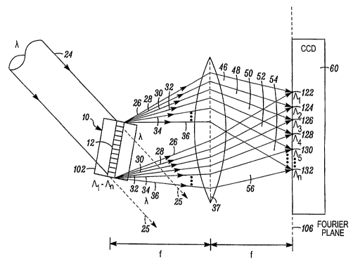
Figure 2a
Fig. 2a shows another example of the Fourier
transform technique similar to the optical arrangement in
Figure 2, wherein an incident light 24 of a wavelength X,
e.g., 532 nm from a known frequency doubled Nd:YAG laser
CA 02587674 2007-05-15
WO 2006/055736 PCT/US2005/041731
11
or 632nm from a known Helium-Neon laser, is incident on a
grating 12 in a substrate 10 of a microbead such as 102
in Figure 2. Any other input wavelength k can be used if
desired provided k is within the optical transmission
range of the substrate (discussed more hereinafter). A
portion of the input light 24 passes straight through the
grating 12 as indicated by dashed lines 25. The remainder
of the light 24 is reflected by the grating 12 and forms
a plurality of beams 26-36, each having the same
wavelength k as the input wavelength k and each having a
different angle indicative of the pitches W-nn)
existing in the grating 12. The reflected light 26-36
passes through a transform lens 37, which is arranged
between the microbead 102 and the Fourier plane 106 at a
distance of about one focal length f from each. The
transform lens 37 provides focused light beams 46-56
which are imaged on the Fourier plane 106 at locations
122, 124, 126, 128, 130, 132 onto a CCD camera 60.
Consistent with that discussed above, instead of or in
addition to the lens 37, other imaging optics may be used
to provide the desired characteristics of the optical
image/signal onto the camera 60 (e.g., spots, lines,
circles, ovals, etc.), depending on the shape of the
substrate and input optical signals. Also, instead of a
CCD camera other devices may be used to read/capture the
CA 02587674 2007-05-15
WO 2006/055736 PCT/US2005/041731
12
output light.
Figure 3: The Microbead or Optical Element 102
Figure 3 shows, by way of example, the microbead 102
including the code 104 in the form of periodic layers of
material with different reflectivity, which is known in
the art. The material having different reflective spaces
104a, 104b, 104c, ..., 104o may include one reflectivity
that may represent a logical "0" (indicated by blank
spaces generally indicated by lead lines 104b, 104e,
104f, etc.), while the material having the other
reflectivity may represent a logical "1" (indicated by
elements 104a, 104c, 104d, etc.), or vice versa. As
shown, the code 104 represents the binomial number "101
110 010 011 001", or "010 001 101 100 110" if the logical
representation of the reflectivity is reversed.
Consistent with that discussed above, the scope of the
invention is not intended to be limited to any particular
code or coding method or technique. Moreover, the scope
of the invention is intended to be used in conjunction
with known coding techniques, coding techniques that form
part of the invention as described herein, as well as
coding techniques later developed in the future.
Alternatively, the code 104 may include periodic
layers of material having a different phase, including
index of refraction differences; periodic spatial
CA 02587674 2007-05-15
WO 2006/055736 PCT/US2005/041731
13
modulations having a different phase or amplitude; a
periodic binary phase change used to code information in
the Fourier plane; a photonic crystal used to encode the
information on the microbead, wherein a pattern of holes
causes interference between incident and scattered light
to form spatial and spectral patterns in the far field
that are unique to the pattern of holes; or may be formed
in the microbead using a single photoactive inner region,
a series of longitudinal holes, different fluorescence
regions, or concentric rings of material in a preform.
In effect, the present invention has applications in
reading any code that is unique and repeatable, including
codes that are otherwise imaged on an image plane in the
prior art in order to be read.
The microbead or optical element 102 may be
microscopic in size having a length in a range of 1-1,000
microns or smaller; or for larger applications may have a
length of 1.0 - 1,000 millimeters or more. The outer
diameter may be as small as less than 1,000 microns, as
well as in a range of 1.0 to 1,000 millimeters for larger
applications. Using manufacturing techniques developed
in conjunction with the development of the present
invention, one optical fiber or substrate can be drawn
and processed to produce hundreds of thousands, as well
as even a million or more of such unique microbeads. The
microbead or optical element 102 may be used in which a
CA 02587674 2007-05-15
WO 2006/055736 PCT/US2005/041731
14
substrate is used such as an optical substrate having the
refractive index of the inner region is less than or
equal to the outer region. By way of example, the reader
is referred to the optical elements disclosed in
provisional patent application serial nos. 60/546,445
(CV-35), 60/546,435 (CV-53), 60/547,013 (CV-65), all
filed on February 19, 2004, as well as application serial
no. 661,836 (CC-652), filed on September 12, 2003, which
are all hereby incorporated by reference. The scope of
the invention is not intended to be limited to the type,
kind, shape or size of the microbead or optical element
102. The scope of the invention is intended to include
optical substrates both now known and later developed in
the future.
Figure 4:
Figure 4 shows an example of a Fourier plane readout
of a multilayer metallic particle, which obviates the
need for a high resolution imaging system. Similar
elements in Figures 2 and 4 are labelled with similar
reference numeral. In this example, the microbead 102
has the code 104 in the form of a periodic spatial
modulation (amplitude or phase) that reflects an incident
light 108 through a transform lens 110 onto the Fourier
plane, where the periodicity causes a "dot" or bit which
may be read and interpreted accordingly.
CA 02587674 2007-05-15
WO 2006/055736 PCT/US2005/041731
It is important to note that, although in principle
analog patterns can be used to encode in the Fourier
plane, it is often advantageous to use only two "levels",
where the levels can be either the phase (index) change
and/or absorption change. For instance, the metallic
layered particles of one known coding technique could be
read out in a Fourier plane, thus obviating the necessity
of a high resolution microscope. Periodic modulations of
phase or amplitude can be "written" into an optical
filament after it is drawn from a preform, allowing
flexibility in the amount of particles that are encoded
in a single batch.
Figures 5 and 6: Other Fourier Scattering
Techniques for Encoding Microbeads
The present invention also provides many different
types of Fourier scattering techniques for encoding
microbeads that can be read using the Fourier plane
analysis technique described herein. For example, many
different geometries of the inner region and/or can be
envisioned that can lead to a uniquely identifiable
marking of the diced microbeads, including: a single
photoactive inner region (Figure 5A), a series of
longitudinal holes (Figure 5B), different fluorescence
regions (Figure 5C), or concentric rings (Figure 5D) of
material in the preform to name a few examples. These
CA 02587674 2007-05-15
WO 2006/055736 PCT/US2005/041731
16
markings or patterns may be formed in the inner region
and/or outer region of an optical filament drawn from a
preform and cut to form the microbeads. These patterns
on the microbeads are unique and repeatable and may be
read using the Fourier plane analysis technique shown and
described herein.
Figure 6 shows still another examples of Fourier
scattering techniques using photonic crystal
microparticles which encode information according to the
present invention. The pattern of the holes causes
interferences between the incident and scattered light to
form spatial and spectral patterns in the far field that
are unique to the pattern of holes. In operation,
incident light is provided to a microbead 102' having a
photonic crystal therein causing a radiation pattern and
spectrum that uniquely encodes information that can be
read using the Fourier plane analysis technique described
herein.
The scope of the invention is not intended to be
limited to any particular pattern formed in the inner
region and/or outer region of the filament being drawn
from a preform using techniques now known or later
developed in the future.
Figure 7: The Imaging Properties
Referring to Fig. 7, the imaging properties of a
CA 02587674 2007-05-15
WO 2006/055736 PCT/US2005/041731
17
known positive lens 402 may be described according to the
following known principles. If an object 404 is located
a distance so away from the lens 402, i.e., in an "object
plane", the lens 402 will form an image 406 in an "image
plane" of the object 404 a distance si away from the lens
402. The known relationship between so and si can be
written as follows:
1 1 1
-+-_-
sm sr f
where f is the focal length of the lens 402 and so is
greater than the focal length of the lens 402. The size
of the image relative to the object (or magnification M)
has the known relationship:
M s;
so
where M is the size of the image 406 divided by the size
of the object 404. Accordingly, if the lens 402 is
placed a distance f away from the object 404, the image
405 is infinitely large at a distance of infinity away
from the lens 402, as is known. For the purposes of this
discussion, the lens 402 is presumed to be infinitely
large, infinitely thin (i.e., a line) as located on a
plane parallel to the plane of the lens, and with no
aberrations.
CA 02587674 2007-05-15
WO 2006/055736 PCT/US2005/041731
18
Figure 8: The Fourier Properties
Referring to Figure 8, the Fourier properties of a
lens 402 may be described based on the following known
principles. If the lens 402 is placed a distance f in
front of an electric field distribution 408, the lens 402
will form an electric field distribution 410 that
corresponds to the Fourier transform of the original
electric field profile 408 at a distance f away from the
lens 402 (i.e., at the "Fourier Plane" 411). The Fourier
Plane image is also known as the "far field" image with a
different scale, e.g., greater than about 20 Rayleigh
ranges away. In particular, for the electric field sine
wave 408 having a predetermined intensity or peak value
and a DC offset, resulting Fourier transform intensity
pattern in the Fourier Plane 411 provided by the lens 402
would be three delta functions (or points of light) 410,
412, 414, corresponding to the DC value at the point 412,
the positive frequency value of the sign wave 408 at the
point 410 and the negative value of the frequency of the
sign wave 4G8 at the point 414. The intensity of the
light at the point 412 corresponds to the DC value of the
sine wave 408, and the intensity of the light at the
points 410, 414 corresponds to the peak value of the sine
wave 408.
Relating the Fourier Plane discussion above to a bar
CA 02587674 2007-05-15
WO 2006/055736 PCT/US2005/041731
19
code printed on a bead or particle such as element 102
(Figure 2) that is read by an optical reader such as
element 112 (Figure 2), the sine wave 408 could
correspond to the bar code on the bead 102 having a
single spatial period, an efficiency < 100%, and where a
light beam 412 is incident on the bead at an angle of 0
degrees to the normal of the grating vector (the
longitudinal axis of the bead 8).
It should be further understood from Figures 7 and 8
that if the lens 402 is placed a distance so away from the
incident electric field 408, the lens would provide an
image of the electric field 408 at a distance si away with
a magnification so/si (not shown).
Accordingly, the present invention detects an image
of the Fourier transform of the bar code on the bead 102
at the Fourier plane, which appears as lines on a CCD
camera (or code camera) in the Fourier plane. As a
result, the reader 112 does not require expensive imaging
optics to obtain an image of the bead 102.
In contrast, as shown in Figure 1, if the code on
the bead 14 was detected by obtaining an image of the
bead 14, e.g., if the code was simply as series of
stripes printed on the bead 14, the reader/detector 20
would need to obtain a magnified image of the bead 14
with sufficient magnification to allow a code camera to
read the stripes and thus obtain the code on the bead 14.
CA 02587674 2007-05-15
WO 2006/055736 PCT/US2005/041731
In this regard, if the appearance of the code on the
bead looks like a bar code or digital code, the image in
the Fourier plane will not look like the bar code or
digital code, it will look like the Fourier transform of
a bar code or digital code seen on the bead. Similarly,
if the image of the code in the Fourier plane looks like
a bar code or digital code, the appearance of the code on
the bead will not likely look like a bar code or digital
code because it will be the inverse Fourier transform of
the bar code or digital code seen in the Fourier plane.
Accordingly, it may be desirable to have the Fourier
plane have a simple digital image that is easy to
identify to keep the detector simple. In that case, the
actual code on the bead itself will likely be
unintelligible as a bar code or digital code.
CA 02587674 2007-05-15
WO 2006/055736 PCT/US2005/041731
21
Figures 9-11: The Readout Beam
A technical requirement of the readout beam
projected on the Fourier plane is that it must have a
spatial coherence Lc large enough to resolve adjacent
frequency components used to identify the object such as
the microbead. Figure 9 shows the relationship between
the spatial coherence length and two adjacent spatial
frequencies (shown schematically on Figure 9.) The
general requirement for the spatial coherence length is
< 1/A1 - 1/A2 -
Figure 10 shows an example of the reflectivity of an
object composed of the spatial frequency components shown
in Figure 11. Information is contained in both the power
amplitude and the spatial frequency of the Fourier
components. A particularly robust method of identifying
an object would be to look at the presence or absence of
particular Fourier spatial frequencies, and choose a
threshold to determine if a particular frequency
corresponds to a logical "1" or a logical "0" (i.e.
digital encoding.) If a threshold of 0.1 is chosen in
the example of Figure 11, then the corresponding digital
code would be 11011 for the five spatial frequencies
analyzed.
CA 02587674 2007-05-15
WO 2006/055736 PCT/US2005/041731
22
Scope of the Invention
The dimensions and/or geometries for any of the
embodiments described herein are merely for illustrative
purposes and, as such, any other dimensions and/or
geometries may be used if desired, depending on the
application, size, performance, manufacturing
requirements, or other factors, in view of the teachings
herein.
It should be understood that, unless stated
otherwise herein, any of the features, characteristics,
alternatives or modifications described regarding a
particular embodiment herein may also be applied, used,
or incorporated with any other embodiment described
herein. Also, the drawings herein are not drawn to scale.
Although the invention has been described and
illustrated with respect to exemplary embodiments
thereof, the foregoing and various other additions and
omissions may be made therein and thereto without
departing from the spirit and scope of the present
invention.
Moreover, the invention also comprises features of
construction, combination of elements, and arrangement of
parts which will be exemplified in the construction
hereinafter set forth.
It will thus be seen that the objects set forth
above, and those made apparent from the preceding
CA 02587674 2007-05-15
WO 2006/055736 PCT/US2005/041731
23
description, are efficiently attained and, since certain
changes may be made in the above construction without
departing from the scope of the invention, it is intended
that all matter contained in the above description or
shown in the accompanying drawing shall be interpreted as
illustrative and not in a limiting sense.