Note: Descriptions are shown in the official language in which they were submitted.
CA 02588035 2009-08-25
WO 2006157829 PCf(US20051940974
TITLE OF THE INVENTION
SCRATCH RESISTANT COATED GLASS ARTICLE INCLUDING
LAYER(S) RESISTANT TO FLUORIDE-BASED ETCHANT(S), AND
METHOD OF MAKING ARTICLE USING COMBUSTION CVD
[0041] This application relates to a coated article including a coating
supported by a glass substrate. The coating includes an anti-etch layer that
is resistant
to fluoride-based etchant(s), and may also include other layer(s) such as a
scratch-
.resistant layer comprising diamond lilm carbon (DLC). Coated articles
according to
different embodiments of this invention may be used as windows or in any other
suitable application.
BACKGROUND OF THE INVENTION
[0442] Unfortunately, vandals have increasingly been turning to glass etchants
as a tool of choice for graffiti. For example, graffiti on glass windows of
subway cars
is commonplace. Vandals have been forming such graffiti on windows of subway
cam buildings, trains, buses and otha glass windows by using glass etchants
winch
are capable of etching glass at locations where such etchants are applied.
[0403] Armor-etch is an example of a bifluorlde salt (e.g., ammonia bifluoride
or sodium bifhnaride) based paste used far etching pattenm on glass surfaces,
and has
been used in forming graffiti. The mechanism of fluoride ion attack on Si0s of
glass
is summarized below for purposes of example only and understanding.
[0004] Though hydrogen fluoride (HF) does not dissociate well, active
hydrogen fluoride pasta reacts with silicate (which forms the matrix for
glass) in the
presence of water as in the following equations:
HPi = HF + F
1
CA 02588035 2009-08-25
WO 2006/057829 PCf!US20051040974
6HF + SiO2 = E2SiF6 + 21320
[0005] An alternative type of glass etching material, which is also a bi-
fluoride based enchant, is sometimes id erred to as B&B etching crbme
manufactured
by B&B Etching Products. Ammonium bifluoride ((NH4)HP2) and sodium bifluoride
(NaH73) salts are very soluble in water. For example, a 2.8 gl100 g solution
of
ammonium fluoride would produce a 1.7 g)100 g solution of hydrofluoric acid
(HP) at
pH 1, with 85% of the fluorine atoms in the form of HF. At higher
concentrations or
higher pH, a significant amount of the HF2 ion is present. Acidified fluorides
can
produce substantial quantities of HP in solution.
!00061 The active ammonia bi-fluoride reacts with silicate in the presence of
water as presented in the following equations:
(NH4)HF2 = (NH4)} +HF2
z =HP+F
6HF + SiO2 = H2SiF6 + 21120
[0007] An equilibrium is established between the reactants and products.
Thus, as hydrogen fluoride is consumed in reacting with the SiO2 of the glass,
more
hydrogen fluoride is produced to Main the equilibrium. The SiO2 etch rate
(ii.e.,
the etch rate of the glass) is linearly related to the HF and HFz
concentrations, and is
not related to the F concentration at any pE
100081 Conventional coatings used for fluoride resistance to protect glass
from
such etchings are polymer-based film. Unfortunately, these coatings are
susceptible
to damage and are not scratch resistant thereby rendering their use in
environments
such as subway can, buses and vehicles undesirable. Moreover, in some cases
the
film can be lifted and the enchant applied under the film.
100091 Scratch resistant coated glass articles are known which utilize a
layer(s) comprising diamond like carbon (DLC) on the glass surface. For
example,
see U.S. Patent Nos. 6,261,693, 6,303,226, 6,280,834, 6,284,377, 6,447,891,
6,461,731, 6,395,333, 6,335,086, and 6,592,992,
While carbon is resistant to fluoride ion
(and B'2') attack, these layers when formed via ion beam deposition techniques
at
2
CA 02588035 2007-05-17
WO 2006/057829 PCT/US2005/040974
very small thicknesses give rise to micro-particulates on the substrate. When
such
layers are very thin in nature, these micro-particles may give rise to
pinholes which
are pathways for the HF to attack the underlying glass. Thus, scratch
resistant coated
articles which utilize only a layer comprising DLC on the glass are sometimes
susceptible to the fluoride based etchant attacks described above.
[0010] In view of the above, it can be seen that there exists a need in the
art
for a scratch resistant coated article which is also resistant to attacks by
fluoride-based
etchant(s).
BRIEF SUMMARY OF EXAMPLES OF THE INVENTION
[0011] A scratch resistant coated article is provided which is also resistant
to
attacks by at least some fluoride-based etchant(s) for at least a period of
time. In
certain example embodiments, an anti-etch layer(s) is provided on the glass
substrate
in order to protect the glass substrate from attacks by fluoride-based
etchant(s). In
certain example embodiments, the anti-etch layer(s) is substantially
transparent to
visible light.
[0012] In certain example embodiments of this invention, the anti-etch layer
may be provided on the substrate over an underlayer(s) of a dielectric
material. In
certain example embodiments, the dielectric underlayer may be formed using
flame
pyrolysis in an atmosphere at or close to atmospheric pressure. The use of
flame
pyrolysis to form the underlayer(s) is advantageous in that the layer(s)
formed using
flame pyrolysis may be formed in an ambient atmosphere which need not be at a
pressure less than atmospheric (as opposed to sputtering for example which is
typically formed in a chamber at a low pressure less than atmospheric). Thus,
expensive sputtering or other low-pressure deposition systems need not be used
to
form this particular layer(s). Moreover, another example advantage is that
such an
underlayer deposited via flame pyrolysis has been found to further improve the
etch
resistance of the coated article by removing or reducing chemical or other
defects on
the glass surface. In particular, it is believed that the flame-pyrolysis
deposited
underlayer removes or reduces chemical defects on the surface on which the
anti-etch
layer is directly provided. Such defects may lead to growth defects in the
anti-etch
3
CA 02588035 2007-05-17
WO 2006/057829 PCT/US2005/040974
layer 2 which can be weak points more susceptible to etchant attack. Thus, the
removal or reduction of such defects via the use of the flame pyrolysis
deposited
underlayer is advantageous in that etch resistance can be surprisingly
improved.
[0013] In certain example embodiments, the anti-etch layer may be provided
on the glass substrate, along with an overlying scratch resistant layer of or
including
diamond-like carbon (DLC). The anti-etch layer may be of or include any
suitable
material, such as for example the material(s) discussed herein.
[0014] In certain example embodiments, the anti-etch layer(s) may comprise
or consist essentially of zirconium oxycarbide, hydrogenated zirconium
oxycarbide,
tin oxycarbide, or hydrogenated tin oxycarbide. In certain example
embodiments, the
optional underlayer(s) may comprise or consist essentially of silicon oxide,
silicon
nitride, and/or the like.
[0015] In certain example embodiments, there is provided a method of making
a coated article, the method comprising providing a glass substrate; using
flame
pyrolysis to deposit at least one layer on the glass substrate; and forming an
anti-etch
layer on the glass substrate over the flame pyrolysis deposited layer.
[0016] In other example embodiments of this invention, there is provided a
coated article comprising a substrate; an underlayer comprising silicon oxide
on the
substrate; and an anti-etch layer comprising at least one material selected
from the
group consisting of: zirconium oxycarbide, tin oxycarbide, indium oxide and
cerium
oxide; and wherein the anti-etch layer is on the substrate over at least the
underlayer
comprising silicon oxide, and wherein the anti-etch layer is resistant to at
least some
fluoride-based glass etchants.
BRIEF DESCRIPTION OF THE DRAWINGS
[0017] FIGURE 1 is a cross sectional view of a coated article according to an
example embodiment of this invention.
[0018] FIGURE 2 is a cross sectional view of a coated article according to
another example embodiment of this invention.
4
CA 02588035 2007-05-17
WO 2006/057829 PCT/US2005/040974
[0019] FIGURE 3 is a cross sectional view of a coated article according to
another example embodiment of this invention.
[0020] FIGURE 4 is a cross sectional view of a coated article according to
another example embodiment of this invention.
[0021] FIGURE 5 is a cross sectional view of a coated article according to
another example embodiment of this invention.
[0022] FIGURE 6 is a cross sectional view of a coated article according to
another example embodiment of this invention.
[0023] FIGURE 7 is a schematic diagram illustrating an example method of
depositing and/or forming an anti-etch layer according to an example
embodiment of
this invention.
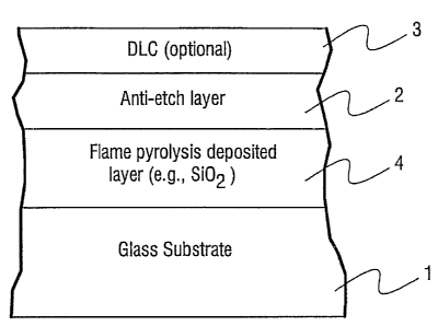
[0024] FIGURE 8 is a cross sectional view of a coated article according to
another example embodiment of this invention.
[0025] FIGURE 9 is a flowchart listing certain example steps performed in
making the coated article of Fig. 8 according to an example embodiment of this
invention.
DETAILED DESCRIPTION OF EXAMPLE EMBODIMENTS OF THE
INVENTION
[0026] Referring now more particularly to the accompanying drawings in
which like reference numerals indicate like parts/layers throughout the
several views.
[0027] Coated articles according to certain example embodiments of this
invention may be used as subway car windows, transit bus windows, train
windows,
or other types of vehicle windows, or the like in different applications.
Coated
articles according to certain example embodiments of this invention may also
be used
as architectural windows, in monolithic or IG unit form. Coated articles such
as
windows according to certain example embodiments of this invention may have a
visible transmission of at least about 15%, more preferably at least about
50%, more
preferably of at least about 60%, and even more preferably of at least about
70%. In
CA 02588035 2007-05-17
WO 2006/057829 PCT/US2005/040974
certain example embodiments of this invention, any of the coated articles
discussed
herein may or may not be heat treated (e.g., thermally tempered).
[0028] A scratch resistant coated article is provided which is also resistant
to
attacks by fluoride-based etchant(s). In certain example embodiments, an anti-
etch
layer(s) is provided on the glass substrate in order to protect the glass
substrate from
attacks by fluoride-based etchant(s). In certain example embodiments, the anti-
etch
layer(s) is substantially transparent to visible light (i.e., the anti-etch
layer if deposited
alone would be transmissive to at least about 60% of visible light, more
preferably at
least about 70% of visible light, and even more preferably at least about 80%
of
visible light).
[0029] In certain example embodiments of this invention, in a multi-layer
stack, a silicon oxide (e.g., Si02) base layer or underlayer is provided for
improving
the fluoride etch protection of float glass or other suitable substrate. The
silicon oxide
base layer may be from about 50 to 1,500 A thick, more preferably from about
100 to
1,000 A thick, in certain example embodiments of this invention. The silicon
oxide
base layer is located on the substrate, and may be located in direct contact
with the
substrate or alternatively there may be layer(s) between the substrate and the
silicon
oxide layer. The silicon oxide inclusive base layer may be produced by various
method, including MSVD and atmospheric pressure combustion chemical vapor
deposition. Other layer(s) in the stack can include a relatively thick
intermediate
optically transparent layer with inherent fluoride etch resistance, which may
be called
in anti-etch layer in certain example instances. The anti-etch layer may be
from about
500 to 5,000 A thick in certain example embodiments. The anti-etch layer may
be of
cerium oxide, indium oxide, zirconium oxycarbide, or tin oxycarbide in certain
example embodiments. On large area products, the silicon oxide layer may be
produced in a standard in-line MSVD coater, or alternatively by using one or
more
linear combustion CVD burners that span the width of the glass substrate, with
the
glass passing under the burners on a conveyor. For two sided coatings, the
burners
can be installed both above the glass and under the glass between supporting
rollers.
[0030] in certain example embodiments of this invention, single or multi-layer
coatings according to example embodiments of this invention are able to resist
HF
6
CA 02588035 2009-08-25
WO 20061057029 PCTIUS200SI140974
attack on glass for twenty-four hours or so with no visible sign of
significant adverse
effect In example embodiments of this invention, such coatings have a dense
structure, are characterized by low pinhole density, and/or are characterized
by
substantial chemical inertness (e.g., forming insoluble fluorides).
10031] In certain example embodiments, the thickness of the anti-etch layer
(see any layer 2 or 2' herein) need not exceed about 0.9 irm (or 9,000 A). In
certain
example embodiments, the thickness of the anti-etch layer (2 or 2) may be from
about
50 to 9,000 A, more preferably from 100-5,000 A. In certain preferred
instances, the
anti-etch layer (2 or 2') is preferably at least about 2,500 A thick, and
still more
preferably from about 3,000 to 5,000A thick. Although the anti-etch layer may
be
thinner than this in certain example embodiments of this invention, if it is
thinner than
this then etch resistance may suffer undesirably. Moreover when it is thicker
than
this range optical properties such as visible transmission or the like may
suffer. We
note however that t is possible for the anti-etch layer to be thicker (e g.,
from 9,000 to
20,000 A) in certain instances.
[00321 Fig. 1 is a cross sectional view of a coated article according to an
example embodiment of this invention. The coated article includes a glass
substrata I
(e.g., soda lime silica glass, or borosilicate glass which may or may mat be
polished)
which supports both an anti-etch layer 2 and a setatch resistant layer 3 of
including
DLC or the like.
[00331 The layer 3 of or including DLC may be any of the DLC inclusive
layers described in one or more of U.S. Patient Noa. 6,261,693, 6,303,226,
6,280,834,
6,284,371, 6,447,891, 6,461,731, 6,395,333, 6,335,086, andlce 6,592,992, and
may be
deposited/formed in any of the manners described in any of these patents.
For example, and
without limitation, DLC inclusive layer 3 may be from about 5 to 1,000
angstroms
(A) thick in certain example embodiments of this invention, mare preferably
from 10-
300 A thick. in certain example embodiments of this invention, layer 3
including
DLC may have an average hardness of at least about 10 ON, more preferably at
least
about 20 CIPa, and most preferably from about 20-90 GPs. Such hardness renders
layer (a) 3 resistant to scratching, certain solvents, and/or the like. Layer
3 may, in
7
CA 02588035 2009-08-25
WO 20061057829 PCTJUS2005/840974
certain example embodimmenta, be of or include a special type of DLC known as
highly tetrahedral amorphous carbon (t-aC), and may be hydrogenated (t-aC:H)
in
certain embodiments (e.g., from 5 to 39% hydrogen, more preferably from 5 to
25%
hydrogen, and most preferably from 5 to 20% hydrogen). This type of DLC
includes
more spa carbon - carbon (C - - C) bonds than spa carbon - carbon (C - - C)
bonds. In
certain example embodiments, at least about 50% of he carbon-carbon bonds in
the
layer 3 may be spa carbon - carbon (C - - C) bonds, more preferably at least
about
60% of the carbon-carbon bonds in the layer 3 may be se carbon - carbon (C - -
C)
bonds, and most preferably at least about 70% of the carbon-carbon bonds in
the layer
3 may be sp3 carbon - carbon (C - - C) bonds. In certain example embodiments
of
this invention, the DLC inclusive layer 3 may have a density of at least about
2.4
gm/cros, more preferably of at least about 2.7 gm/cm3. Example linear ion beam
sources that may be used to deposit DI C inclusive layer 3 on substrate 1 via
an ion
beam include any of those in any of U.S. Patent Nos. 6,359,388, 6,261,693.
6,002,208, 6,335,086, 6, 303,226, or 6,303,225,
When using an ion beam source to deposit layer(s) 3, hydrocarbon feedstock
gas(es)
(e.g., Cam}, HMDSO, or any other suitable gas, may be used in the ion beam
source
in order to cause the source to emit an ion beam toward substrate 1 for
foaming DLC
inclusive layer(s) 3. It is noted that the hardness and/or density of layer(s)
3 may be
adjusted by varying the ion energy of the depositing apparatus. The use of DLC
inclusive layer 3 allows the coated article (e.g., monolithic window, or 10
unit) to be
more scratch resistant than if the coating were not provided.
[00341 In certain example embodiments of this invention, the glass substrate I
may be ion beam milled before the anti-etch layer 2 (or layer 4) is deposited
thereon.
The ion beam milling of the glass substrate has been found to remove certain
defects
on the glass surface thereby resulting in a more durable end product. Por
example and
without limitation, any of the example techniques of ion beam milling
described in
U.S. Patent No. 6,368,664 may be used to ion beam mill the glass substrate I
in this
regard. In the Pig. 1
embodiment for example, after ion beam milling the glass substrate (e.g.. to
remove at
least about 2 A of glass from the substrate, more preferably at least about 5
A, and
possibly at least about 10 A), the anti-etch layer 2 may be deposited using
magnetron
8
CA 02588035 2007-05-17
WO 2006/057829 PCT/US2005/040974
sputtering or IBAD in different embodiments of this invention. Thereafter, the
DLC
inclusive layer 3 may be ion beam deposited over the anti-etch layer 2. Stack
configurations may be produced by one-pass in-line deposition in a suitably
configured system, or in any other suitable manner.
[0035] Anti-etch layer(s) 2 is provided to allow the coated article to be
resistant to attacks by fluoride-based etchant(s) such as those discussed
above. The
anti-etch layer 2 may be deposited by sputtering, ion beam deposition, or ion
beam
assist deposition (IBAD) in different embodiments of this invention. Anti-etch
layer
2 substantially prevents (or reduces) fluoride-based etchant(s) such as those
discussed
above from reaching the glass substrate 1 for at least a period of time (e.g.,
for at least
one hour, more preferably for at least twelve hours, and most preferably for
at least
twenty-four hours), thereby rendering the coated article more resistant to
attacks by
fluoride-based etchant(s) such as those discussed above. Moreover, since
certain
embodiments of this invention are used in the context of window applications,
the
anti-etch layer(s) 2 is substantially transparent to visible light.
[0036] It has been found that the inclusion of carbon into an inorganic layer
2
or coating significantly improves the resistance of the coated glass article
to corrosion
by fluoride etching. In certain example embodiments, at least carbon inclusive
reactive gas (e.g., acetylene (C2H2) and/or C02) is used during the deposition
process
of anti-etch layer 2 in order to provide carbon in the resulting layer thereby
improving
the corrosion resistance of the layer and the coated article. As shown in Fig.
1, the
anti-etch layer 2 may comprise or consist essentially of zirconium oxycarbide
(e.g.,
ZrOC), zirconium carbide (ZrC), hydrogenated zirconium oxycarbide (e.g.,
ZrOC:H),
and/or hydrogenated zirconium carbide (e.g., ZrC:H). These materials are
advantageous in that zirconium carbide is very scratch resistant, thereby
improving
the mechanical durability of the coated article in addition to being etch
resistant. In
this respect, zirconium carbide (even if it also includes oxygen) tends to be
a very
hard and durable material. In certain example embodiments of this invention,
the
zirconium carbide inclusive layer 2 may be formed (e.g., via sputtering or
IBAD) so
as to have an average hardness of at least about 20 :;Pa, more preferably of
at least
9
CA 02588035 2007-05-17
WO 2006/057829 PCT/US2005/040974
about 25 GPa, still more preferably of at least about 27 GPa, and most
preferably of at
least about 29 GPa.
[0037] Moreover, another advantage associated with these materials is that
zirconium carbide (whether or not hydrogenated and/or oxided) is fairly
resistant to
oxidation in environments where it is exposed to W rays and/or water - this is
an
improvement over DLC alone in certain example non-limiting embodiments of this
invention.
[0038] It has surprisingly been found that when Zr (or Sn as discussed below)
is reactively sputter-deposited or otherwise deposited using a carbon
inclusive gas
such as C2H2 plus 02, or CO2 (optionally in addition to Ar gas for example),
the
resulting coating and coated article realizes significantly improved
resistance to
fluoride based etching compared to a situation where the Zr (or Sn) is
reactively
deposited using only 02 gas (in addition to Ar). It is believed that the
surprisingly
improved resistance resulting from the inclusion of carbon in the gas and thus
the
layer is due to the carbon's inert characteristics. While these surprisingly
results are
associated with Zr, the Zr may be replaced with any of the following materials
in any
layer 2 herein: Sn, Ti, Hf, V, Nb or Ta (it is expected that these
surprisingly results
will also be applicable to these materials).
[0039] As mentioned above, the ZrC or ZrOC may be hydrogenated in certain
example embodiments of this invention. In hydrogenated embodiments (e.g.,
ZrC:H
or ZrOC:H), the hydrogen content of the layer may be from about 1-40%, more
preferably from about 5-35%, and even more preferably from about 5-25%.
[0040] As explained above, when the DLC layer is provided, it is typically
deposited by an ion beam technique over the Zr inclusive anti-etch layer 2. In
such
instances, due to the high energy which may be used in ion beam depositing DLC
inclusive layer 3, the DLC may alloy with the Zr at the interface between
layers 2 and
3. Thus, a thin layer comprising an alloy of Zr and DLC may be provided
between
layers 2 and 3 in certain example embodiments of this invention.
[00411 Fig. 2 illustrates another example embodiment of this invention where
an underlayer 4 (e.g., silicon nitride, silicon oxide {e.g., SiO2 or any other
suitable
stoichiometry}, or silicon oxynitride) is provided between the glass substrate
1 and
CA 02588035 2009-08-25
WO 2006/057824 PCTIUS20051840974
the anti-etch layer 2 discussed above. Of course, any of the aforesaid anti-
etch layers
2 may be used as layer 2 in this embodiment. In certain example instances, the
underlayer 4 (which is preferably a dielectric) has been found to further
improve the
etch resistance of the coated article by removing or reducing chemical or
other defects
on the glass surface. In particular, it is believed that the underlayer 4 of
silicon oxide
for example removes or reduces chemical defects on the surface on which the
anti-
etch layer is directly provided. Such defects may lead to growth defects in
the anti-
etch layer 2 which can be weak points more susceptible to etchant attack.
Thus, the
removal or reduction of such defects via the use of silicon oxide or the like
is
advantageous in that etch resistance can be surprisingly improved. The silicon
oxide
or the like of the underlayer 4 maybe formed in any suitable manner, such as
by
magnetron sputtering, flame pyrolysis (combustion-CVD) . An example
advantage of flame pyrolysis or combustion-CVD is that it is an atmospheric
pressure
process and does not require expensive hardware typically associated with low
pressure processes such as spottering.
10042] In certain example embodiments of this invention, any of the
underlayers 4 may have a thickness of from about 30 to 800.x, more preferably
from
about 50 to 500 A. and most preferably from about 100 to 400 A.
[0043] Fig. 3 illustrates another example embodiment of this invention where
the anti-etch layer 2 alone is provided on the glass substrate. There need not
be any
protective layer over the anti-etch layer 2 in this embodiment. Again, any of
the
aforesaid anti-etch layers 2 may be used as layer 2 in this Fig. 3 embodiment.
In other
words, the anti-etch layer 2 in the Mg. 2-3 embodiments maybe made of or
include
any of the materials listed above with respect to layer 2 in the Hg. 1
embodiment
[00441 It has been found that the deposition temperature for the and-etch
layer
2 may in certain instances play a role in etch resistance. In certain example
instances,
sputter-depositing anti-etch layer 2 at elevated temperatures results in
unexpectedly
improved etch resistance. In certain example embodiments, the anti-etch layer
2 (or
2jis deposited by sputtering onto a glass substrate 1 (with or without an
underlayer(s)
4 t mbetween) at a temperature of at least about 100 degrees C, more
preferably of
at least 200 degrees C, still more preferably at least 300 degrees G even more
11
CA 02588035 2007-05-17
WO 2006/057829 PCT/US2005/040974
preferably of at least 400 degrees C, and sometimes at least 450 degrees C. It
is
believed that the higher temperatures increase the energy provided during the
layer
formation process and increase the density of the layer thereby improving anti-
etch
characteristics. However, in other example instances, elevated temperatures
are not
used and the deposition may take place at room temperature or the like.
[0045] As an alternative to using high temperatures when forming the anti-
etch layer, the anti-etch layer 2 may be formed using IBAD in certain example
embodiments of this invention. Again, the advantage of using IBAD is that the
ion
beam(s) used during IBAD layer formation adds energy to the layer formation
process
and causes a more dense layer to be formed. Again, it is believed that this
improves
anti-etch characteristics of the layer 2. In an IBAD process, both an ion
beam(s) and
material from a sputtering target(s) simultaneously impinge on the substrate
in order
to form the layer being deposited. Fig. 7 illustrates and example of using
IBAD to
form/deposit anti-etch layer 2. As shown, in this IBAD embodiment both an ion
beam source(s) 26 and a sputtering device including a sputtering target(s) 50
are used.
An ion beam B from the ion beam source 26 intersects with the material M
sputtered
from the sputtering target(s) 50 proximate the surface where at least part of
the anti-
etch layer 2 (or 2') is being grown, so that at least part of the anti-etch
layer 2 is
grown/formed by a simultaneous combination of both the ion beam and
sputtering.
Substrate 1 is preferably moving in direction D during the layer formation
process.
[0046] In a pure sputtering embodiment where anti-etch layer 2 (or 2') is
formed by sputtering only with no ion source, or alternatively in the Fig. 7
IBAD
embodiment, gas including carbon such as gas comprising C2H2 and/or CO2 may be
introduced to a sputtering chamber proximate the sputtering target 50 (e.g.,
of Zr, Sn
or the like) so that a layer 2 comprising ZrC:H and/or ZrC is formed on
(directly or
indirectly) the substrate 1. It will be appreciated that when it is desired to
hydrogenate the layer, the gas should include hydrogen and may comprise a
hydrocarbon gas for example (e.g., C2H2). In addition to the carbon inclusive
gas,
gas(es) such as Ar and/or 02 may also be introduced into the sputtering
chamber
proximate target 50. When 02 gas is also introduced in addition to C2H2 and/or
CO2
gas proximate the target 50, then a layer 2 comprising ZrOC:H and/or ZrOC is
formed
12
CA 02588035 2007-05-17
WO 2006/057829 PCT/US2005/040974
on (directly or indirectly) the substrate 1. An example gas introduction is 90
sccm of
Ar gas and 20 sccm of C2H2 gas being introduced into the sputter zone
proximate the
target 50. The sputter zone is typically at a pressure less than atmospheric
pressure
(e.g., at 2 to 3 mTorr). Moreover, when ion source 26 is used in the formation
process
for layer 2, then gas such as Ar and/or C2H2 may be introduced into the ion
source 26.
In such situations, the ion source 26 may emit ions such as Ar ions, C ions
and/or H
ions in beam B toward the layer formation area on the substrate.
[0047] As explained above, while Zr is used as a metal in the embodiments of
Figs. 1-3, this invention is not so limited unless expressly claimed. In this
respect,
Figs. 4-6 emphasize that the Zr in any of the embodiments described herein, or
shown
in Figs. 1-3, may be replaced with Sn in certain example embodiments of this
invention.
[0048] It is noted that any of the aforesaid materials for anti-etch layers 2
(or
2') may also be nitrided in certain example embodiments of this invention. In
particular, nitrogen gas may also be used in the sputter-deposition process
for
example in order to at least partially nitride the anti-etch layer in certain
alternative
embodiments of this invention. For example, and without limitation, the anti-
etch
layer 2 may comprise or consist essentially of zirconium carbide oxynitride
(e.g.,
ZrCON), zirconium carbide nitride (ZrCN), hydrogenated zirconium carbide
oxynitride (e.g., ZrCON:H), and/or hydrogenated zirconium carbide nitride
(e.g.,
ZrCN:H).
[0049] Fig. 8 is a cross sectional view of an example coated article,
generally
speaking according to an example embodiment. The anti etch layer 2 (or 2') may
be
made of or comprise one or more of the following materials in certain
embodiments
of this invention. Example materials, resistant to attacks by fluoride-based
etchant(s),
which may be used for layer 2 (or 2') include: nitrides of Al, Si, Nb, Cr
and/or Ni,
oxides of Al, Si, Ge, Mg, Nb, Mn, V, W, Hf, Ce, and/or Sn, carbides of Si
and/or W,
fluorides of Mg, Ba and/or Ca, borides of Zr, Ni, Co and/or Fe, oxides of Mo,
In, Ta,
Ni, Nb, Cu, Moln, MoTa, and/or NiCu, and oxynitrides of Mo, In, Ta, Ni, Nb,
Cu,
Moln, MoTa, and/or NiCu. Other possible materials for any anti-etch layer 2
(or 2')
herein include zirconium oxycarbide (ZrO,,Cy), tin oxycarbide (SnOxCy),
zirconium
13
CA 02588035 2009-08-25
WO 20061157829 PCTIUS2003f040974
nitride carbide (ZrN,~Cy), andlor tin nitride carbide (SnxNC,,). The DLC
inclusive
layer 3 is optional.
[0050] Moreover, in the Pig. 8 embodiment, the dielectric underlayer 4 is
formed using flame pyrolysis in an atmosphere at or close to atmospheric
pressure.
Thus underlayer 4 formed in such, a manner is of a material such as silicon
oxide (e.g.,
SiO2). The use of flame pyrolysis to form the undedayer(s) is advantageous in
that
the layer(s) formed using flame pyrolysis may be formed in an ambient
atmosphere
which need not be at a pressure less than atmospheric. Thus, expensive
sputtering or
other low-pressure deposition systems need not be used to form this particular
layer(s). Moreover, another example advantage is that such an underlayer
deposited
via flame pyrolysis has been found to further improve the etch resistance of
the coated
article by removing or reducing chemical or other defects on the glass
surface. In
particular, it is believed that the flame-pyrolysis deposited underlayer 4
rmoves or
reduces chemical defects on the surface on which the anti-etch layer is
directly
provided. Such defects may lead to growth defects in the anti-etch layer 2
which can
be weak points more susceptible to etchant attack. In c main respects, the
flame-
pyrolysis deposited layer (e.g.. silicon oxide) 4 acts as a barrier layer to
prevent
certain defects andloor dements present at the glass surface (e.g., sodium,
protrusions,
etc.) from teaching and damaging the salt-etch layer. Tus, tree removal or
mdzrction
of suds defects via the use of the flame pyrolysis deposited underlayer is
advantageous in that etch resistance can be surprisingly unproven
[9052] For purposes of example, and without limitation, consider the
following examples of flame pyrolysis which may be used in certain embodiments
of
the instant invention to form a layer(s) 4 an the glass substrate. A
combustion gas or
fuel gas such as propene, and a silicon inclusive compound such as SiH4,
otganosilane, tetthnxy3i2ane (TWOS). RMDSO, organosiloxanF may be
introduced into the flame in order to cause a thin layer 4 of silicon oxide to
form on
the substrate 1, either directly or indirectly. The silicon oxide may include
small
amounts of other elements in certain instances. Other examples of flame
pyrolysis are
described in U.S. Patent Nos. 4,600,390, 4,620,988, 3,883,336, and 5,958,361,
14
CA 02588035 2007-05-17
WO 2006/057829 PCT/US2005/040974
[0052] Fig. 9 is a flowchart illustrating certain example steps performed in
making the coated article of Fig. 8. First, after a glass substrate 1 is
provided, flame
pyrolysis is used to deposit a base layer 4 of silicon oxide or the like on
the substrate
(S 1). Then, the anti-etch layer 2 is formed on the substrate 1 over the base
layer 4, via
sputtering or the like (S2). Then, optionally, a scratch resistant layer 3 of
a material
such as DLC is formed on the substrate 1 over layers 2, 4.
EXAMPLES
[0053] The following examples are provided for purposes of example only
and are not intended to be limiting unless expressly claimed.
[0054] Examples 1 and 2 formed a Zr inclusive layer using a Zr sputtering
target on a glass substrate. The Example 1 layer was of ZrO and had no carbon,
whereas the Example 2 layer was of ZrOC:H and thus did include carbon. By
comparing Examples 1 and 2, it can be seen that the provision of carbon in the
layer
significantly improve corrosion resistance of the layer. The layers of
Examples 1 and
2 were deposited on the glass substrate 1 using the following sputtering
process
parameters. The parameters Ar, 02, C02, C2H2, and N2 illustrate how much gas
flow
was used in the sputtering process in the sputtering chamber atmosphere for
each of
these gases, in units of sccm. In each of Examples 1-2, a power of 8 kW was
used, 9
passes by the target were performed, the line rate was about 15.4 inches per
minute.
The layer deposited in Example 1 ended up about 102 nm thick, whereas the
layer in
Example 2 ended up about 265 nm thick.
Examples 1-2 (Sputtering Process Parameters - Zr target)
Ar 02 CO2 C2H2 N2
Ex.l 200 75 0 0 0
Ex.2 200 0 50 50 0
[0055] Thus, it will be appreciated that given the gases used in sputtering
the
Zr inclusive layers in Examples 1 and 2, the Example 1 layer was of ZrO and
had no
carbon, whereas the Example 2 layer was of ZrOC:H since carbon dioxide and
acetylene gases were used and thus did include carbon. The Example 1 coated
article
CA 02588035 2007-05-17
WO 2006/057829 PCT/US2005/040974
had a visible transmission of about 75%, whereas the Example 2 coated article
had a
visible transmission of about 66%.
[0056] Examples 1-2 were then exposed to a fluoride etchant for the same
amount of time in order to compare the corrosion resistance of the two layers.
Surprisingly, it was observed that after about 3 minutes of exposure to the
etchant,
about 100% of the Example 1 layer had been removed whereas about 0% of the
Example 2 layer had been removed. Moreover, after about 10 minutes of exposure
to
the etchant, only about 5% of the Example 2 layer had been removed due to the
etchant, mostly via pinholes. Thus, it can be seen by comparing Examples 1 and
2,
that the provision of carbon in the layer significantly improve corrosion
resistance of
the layer. In particular, the Example 2 layer with carbon was much more
resistant to
corrosion than was the Example 1 layer without carbon.
[0057] Examples 3 and 4 are additional examples of certain embodiments of
this invention, where Zr inclusive anti-etch layers 2 were deposited on a
glass
substrate 1 via sputtering using Zr sputtering targets. In each of Examples 3-
4, a
power of 8 kW was used, 9 passes by the target were performed, the line rate
was
about 15.4 inches per minute. The layer deposited in Example 3 ended up about
285
nm thick, whereas the layer in Example 4 ended up about 172 nm thick.
Examples 3-4 (Sputtering Process Parameters - Zr target)
Ar 02 CO2 C2H2 N2
Ex.3 200 10 0 50 50
Ex.4 200 25 0 50 50
[0058] Thus, it will be appreciated that given the gases used in sputtering
the
Zr inclusive layers in Examples 3 and 4, each of the anti-etch layers 2 of
Examples 3
and 4 was of hydrogenated zirconium carbide oxynitride (e.g., ZrCON:H). The
Example 3 coated article had a visible transmission of about 21%, whereas the
Example 4 coated article had a visible transmission of about 57%. Examples 3-4
were then exposed to a fluoride etchant for the same amount of time in order
to
compare the corrosion resistance of the two layers. Surprisingly, it was
observed that
after about 3 minutes of exposure to the etchant, about 0% of the Example 3
layer and
16
CA 02588035 2007-05-17
WO 2006/057829 PCT/US2005/040974
about 0% of the Example 4 layer had been removed. Moreover, after about 10
minutes of exposure to the etchant, only about 5% of the Example 4 layer and
0% of
the Example 3 layer had been removed due to the etchant.
[0059] Examples 5 and 6 formed a Sn inclusive layer using a Sn sputtering
target on a glass substrate. The Example 5 layer was of SnO (probably a
version of
SnO known as Sn02) and had no carbon, whereas the Example 6 layer was of SnOC
and thus did include carbon and did not include hydrogen. By comparing
Examples 5
and 6, it can be seen that the provision of carbon in the layer significantly
improve
corrosion resistance of the layer. The layers of Examples 5 and 6 were
deposited on
the glass substrate 1 using the following sputtering process parameters. The
parameters Ar, 02, C02, C2H2, and N2 illustrate how much gas flow was used in
the
sputtering process in the sputtering chamber atmosphere where the target was
located
for each of these gases, in units of sccm. In Example 5 a power of 20 kW was
used
and in Example 6 a power of 5 kW was used. In each of Examples 5-6, 1 pass by
the
target was performed, and the line rate was about 15.4 inches per minute. The
layer
deposited in Example 5 ended up about 79 nm thick, whereas the layer in
Example 6
ended up about 45 nm thick.
Examples 5-6 (Sputtering Process Parameters - Sn target)
Ar 02 CO2 C2H2 N2
Ex.5 250 550 0 0 0
Ex.6 250 0 460 0 0
[0060] Thus, it will be appreciated that given the gases used in sputtering
the
Sn inclusive layers in Examples 5 and 6, the Example 5 layer was of SnO and
had no
carbon, whereas the Example 6 layer was of SnOC since carbon dioxide was used
and
thus did include carbon. The Example 5 coated article had a visible
transmission of
about 74%, whereas the Example 6 coated article had a visible transmission of
about
70%.
[0061] Examples 5-6 were then exposed to a fluoride etchant for the same
amount of time in order to compare the corrosion resistance of the two layers.
Surprisingly, it was observed that after about 3 minutes of exposure to the
etchant,
17
CA 02588035 2009-08-25
WO 2006/057829 PC MS20051040974
about 15% of the Example 5 layer had been removed whereas only about 10% of
the
Example 6 layer had been removed. 'Thus, it can be seen by comparing Examples
5
and 6, that the provision of carbon in the layer improved corrosion resistance
of the
layer. In particular, the Example 6 layer with carbon was more resistant to
corrosion
than was the Example 5 layer without carbon.
[0062] A flame pyrolysis deposited dielectric layer (e.g., silicon oxide) may
be formed between the glass substrate and the anti-etch layer in any of
Examples 1-6.
(0063] Examples 7-8 illustrate example advantages associated with the use of
an underlayer 4 of silicon oxide under an anti-etch layer 2 on a float glass
substrate 1.
For Example 7, a MSVD SiO2 layer about 100 A thick was deposited on a float
glass
substrate. An anti-etch layer of cerium oxide was then deposited on the
substrate over
the SiO2layer, and fluoride based etch resistance testing was performed using
Armor
Etch. Comparing samples (Example 8) without the SiO2 layer with samples
(Example
7) with the SiO2 layer, much less damage (primarily in the form of pinholes)
was
observed on the sample (Example 7) having the SiO2 layer under the anti-etch
layer.
Thus, the unexpected advantages associated with the use of the silicon oxide
underlayer 4 are clear.
[00641 While the invention has been described in connection with what is
presently considered to be the most practical and pteferned embodiment, it is
to be
understood that the invention is not to be limited to the disclosed
embodiment, but on
the contrary, is intended to cover various modifications
included within the scope of the appended claims.
I8