Note: Descriptions are shown in the official language in which they were submitted.
CA 02588062 2007-05-16
WO 2006/053436 PCT/CA2005/001753
-1-
TtTLE OF THE OF THE '1NVENTION
CROSSTALK REDUCING CONDUCTOR AND CONTACT CONFIGURATION
IN A COMMUNICATION SYSTEM
BACKGROUND TO THE INV NF TION
(001] The present invention relates to a crosstalk reducing conductor and
contact configuration in a communication,system. In particular, the present
invention relates to positioning emitting a receiving conductive paths in a
communication system in order to reduce NEXT, FF-XT, Alien ~NEXT, Alien
FEXT and increase Signal to Noise Ratio (SNR).
13ACKGROUND OF THE INVENTION
[402] Assembiies for transmitting telecommunications signals at high
frequencies via twisted pairs of conductors currently use a variety of means,
such as shielding and the like to ensure that the interference (such as Afien
NEXT) between adjacent cables and connectors in a system is minimised.
These prior art systems typically suffer from the drawback that the redtaction
in Aiien NEXT between adjacent cables and connectors is insufficient for data
transfers at and above 10 gigabits per second. In particular, existing designs
for ports (or jacks) are sufficient to achieve only about a 5508 SNR, which is
insufficient to meet the proposed 70ds SNR necessary for the proposed 10gig
development standard.
SUMMARY OF THE INVENTION
[003] In order to overcome the above and other drawbacks there is provided
a method for reducing cross talk between first and second cables in a data
transmission system, each of the cables comprised of a pair of conductors.
The method comprises the steps of providing a first contact interconnected
with a first conductor of the pair of conductors of the first cable, wherein
the
first contact emits a first signal, providing a pair of contacts, each of the
pair of
CA 02588062 2007-05-16
WO 2006/053436 PCT/CA2005/001753
-2-
contacts interconnected with a different conductor of the pair of r,.onductors
of
the second cable, and positioning the first contact relative to the pair of
contacts such that an amplitude of the signa{ received at one of the second
pair of contacts is substantially the same as an amplitude of the signal
received at another of the second pair of contacts.
[004J There is also provided a method for reducing cross talk between first
and second cables in a data transmission system, each of the cables
comprised of a pair of conductors. The method comprises the steps of
providing a pair of contacts, each of the pair of contacts interconnected with
a
different conductor of the pair of conductors of the first cable, wherein one
of
the pair of contacts emits a first signal which is substantially an inverse of
a
second signal emitted qy another of the pair of contacts, providing at least
one
first contact interconnected with one of the pair of conductors of the second
cable, and positioning the pair of contacts relative to the first contact such
that
an amplitude of the first signal received by the first contact is
substantialky
opposite to an amplitude of the second signal received by the first contact.
[0051 Furthermore, there is provided an assembly for terminating first and
second cables in a telecommunications system, each of the cables
comprising first and second conductors, the assembly c4mprising a first
contact interconnected with the first conductor of the first cable, wherein
the
first contact emits a first signal, and a pair of contacts interconnected with
a
respective one of the first and second conductors of the second cable- The
first contact is positioned relative to the pair of contacts such that an
amplitude of the first signal received at one of the pair of contacts is
substantiaAy the same as an amplitude of the first signal received at another
of the pair of contacts.
[006] Additionally, there is provided an assembly for terminating first and
second cables in a telecommunications system, each of the cables
comprising a pair of conductors, the assembly comprising a pair of contacts
interconnected with the pair of conductors of the first cable, wherein one of
the pair of contacts emits a first signal which is substantially an inverse of
a
CA 02588062 2007-05-16
WO 2006/053436 PCT/CA2005/001753
-3-
second signal emitted by another of the pair of contacts, and a first contact
interconnected with a first conductor of the pair of conductors of the second
cable. The pair of contacts is positioned relative to the first contact such
that
an amplitude of the first signal received by the, first contact is
substantially
opposite to an amplitude of the second signal received by the second contact.
[007] There is also provided an assembly for terminating first and second
cables in a telecommunications system, each of the cabies comprising a pair
of conductors, the assembly comprising a first substantially flat contact
interconnected with one of the pair of conductors of the first cable, and a
second substantially flat contact Interconnected with one of.,the pair of
cQnductors of the second cable, wherein the first contact is arranged at rrght
angles to the second contact.
[008] Additionally, there is provided an assembly for terminating first and
second cables in a telecommunications system, each of the. cables
comprising a pair of conductors, the assembly comprising a first contact
interconnected with one of the pair of conctuctor$ of the, first cable, and a
pair
of contacts interconnected vrith a respective one of the pair of conductors of
the second cable, the;pair of contacts positioned symmetrically about the
first
contact.
[0091 Also, there is provided a connector for terTninating a cable comprising
first and second pairs of conductors, the connector comprising a first contact
interconnected With a conductor of the first pair of conductors, and a pair of
contacts interconnected with a respective one of the second pair of
conductors, the pair of contacts positioned symmetrically about the first
contact.
(0101 Furthermore, there is also provided a connector for terminating a cable
comprising first and second pairs of conductors, the connector comprising a
first substantially flat contact interconnected with a conductor of the first
pair
of conductors, and a second substantially flat contact interconnected with a
CA 02588062 2007-05-16
WO 2006/053436 PCT/CA2005/001753
_ ,~ _
first conductor of the second pair of conquctors, the first flat contact
substantialry at right angles to the second flat contact.
[011] Additionally, there is provided -a method for reducing cross talk in a
data transmission system. The method comprises the steps of provfding a first
transmission path comprised of at least one conductor, the first conductor
emitti.ng a$ignal, providing a second transmission path comprised of a
second pair of conductors, positioning the first conductor relative to the
-second pair of conductors such that an amplitude of the signal received at
one
of the second pair of conductors is substantially the same as an amplitude of
the signal _received at another of the second pair of conductors:
10121 There is also provided a method for reducing cross talk in a data
transmission system. The method comprises the steps of providing a first
transmission path compdsed of a first conductor, providing a second
transmission path comprised of pair of conductors, wherein one of the pair of
conductors emits a first signal which is substantially an inverse of a second
signal emitted by another of the pair of conductors, and positioning the pair
of
conductors relative to the first conductor such that an amplitude of the first
signal received by the first conductor is substantially opposite to an
amplituqe
of the second signal received by the first conquctor.
[0131 Additionally, there is provided an assembly for transmitting data
comprising a first transmission path compFised of a first conductor, the first
conductor emitting a first signal, and a second transmission path comprised of
a pair of conduetors. The first conductor is positioned relative to the pair
of
conductors such that an amplitude of the first signal received at one of the
pair of conductors is substantially the same as an amplitude of the first
signal
received at another of the pair of conductors.
[014] There is furthermore provided an assembly for transmitting data
compdsing a first transmission path comprised of a first conductor, and a
second transmission path comprised of pair of conductors, wherein one of the
pair of conductors emits a first signal which is substantially an inverse of a
CA 02588062 2007-05-16
WO 2006/053436 PCT/CA2005/001753
-5-
second signal emitted by another of the pair of conductors, wherein said first
conductor is positioned relative to the pair of conductors such that an
amplitude of the first signal received by the first conductor is substantially
opposite to an amplitude of the second signal received by the first conductor.
10151 There is also provided a data transmission cable comprising a first
conductor, a pair of conductors arranged in parallel to the first conductor,
and
a cable jacket surrounding the first conductor and the pair of conductors. A
distance between the first conductor and each of the pair of conductors is
substantially the same.
[0161 There is also provided a data transmission cable comprising first pair
of
parallel conductors aligned on a first plane, and a second pair of conductors
aligned on a second plane. The first plane is substantially at right angles to
the second plane and the first plane intersects the second plane along an axis
substantiafly between the second pair of conductors.
[017] Additionally, there is provided a separator spline for separating pairs
of
conductors in a communication cable, the spline comprising an elongate main
portion having four sides, and a conductive pair receiving slot moulde.d
lengthwise in :each side of the main portion. The moulded main portion has
fylfot cross shaped transverse cross section-
RRIEF DESCRIPTION OF THE DRAWINGS
[018] Figures 1A through 1C provide transverse cross sectional views of
conductors in accorqance with an illustrative embodiment of the present
invention;
[019] Figures 2A and 2B provide transverse cross sections of emitting and
receiving conductors in accordance with an illustrative embQdiment of the
present invention;
CA 02588062 2007-05-16
WO 2006/053436 PCT/CA2005/001753
-8-
[020] Figures 3A through 3C provide transverse cross sections of conductor
configurations in accordance with an alternative and first and second
illustrative embodiments of the present invention;
[021] Figures 4A and 4B provide transverse cross sections of cable
configurations In accordance with third and fourth alternative illustrative
embodiments of the present invention;
[022] Figure 5 provides a side perspective view of a connector jack and
cable in accordance with a fifth altemative illustrative ernbodiment of the
present invention;
[0231, Figure,6 provides a side plan view of a twisted pair cable connected to
the connector jack rear panel of'Figure 5;
[0241 Figure 7 schematically illustrates the general electromagnetic radiation
pattern generated 'by a standard Insulation Displacement Connector (IDC) in
the presenee=of an electric potential;
;[025] Figures 8A and 8S schematically illustrate connector configurations for
reduced ANEXT and AFEXT in accordance with sixth and seventh altemative _
illustrative embodiments of the present invention;
.[026] Figure 9 schematicaliy illustrates alternative palanced pair
configurations for reduced crosstalk in accordance with a series of altemative
illustrative embodiments of the present invention;
[027] Figure 10 schematically illustrates aitemative connector or port
configurations for reduced crosstalk in accordance with a series of altemative
illustrative embodiments of the present invention; and
[028] Figure 11 schematically illustrates a possiple periodic connector
configuration for reduced ANEXT and AFEXT in accordance with an
illustrative embodiment of the present invention.
CA 02588062 2007-05-16
WO 2006/053436 PCT/CA2005/001753
_7~
DETAILED DESCRIPTION OF THE ILt_USTRATIVE EMBODIMENTS
[029] Referring now to Figure 1A, as known in the art, as a signal (not
shown) propagates along a first conductor 2 (viewed in transverse cross
section in Figure 3) the time varying currents within the conductor give rise
to
an electromagnetic field (or signal) 4in the free space surrounding the
conductor 6, that is the first conductor 2 acts in a fashion similar to a
transmitting antenna. Additionally, placing a second 6 conductor within this
electromagnetic field 4 induces time varying currents within the second
conductor 6, or in other words this second conductor 6 acts in a fashion
similar to a receiving antenna (in other words, the second conductor 6 is
coupled. to the first conductor 2).
10301 Referring now to Figure 113, in telecommunications systems, where
signals are typically transmitteq along transmission paths comprised of one or
=more pairs of conductors as in S. 10 (again viewed in transverse cross
section) the induction of time varying currents by the conductors of a first
pair
8'in the conductors of the second pair 10 arises as noise on the signals being
transmitted. along the second pair 10, with a similar effect occurring in the
opposite, direction due to the signals being transmitted along the second pair
10. In high speed implementations, and as will be understood by a person of
qrdinary skill in the art, this noise can have a significant negative.impact
on
the quality of the transmitted signals_ Removal or reduction of this
noiseteads
to a decrease in error rates and an increase in data throughput.
[031] Still referring to Figure 1 B, as the coupling effect between
transmission
paths is much more acute for conductors which are arranged in parallel
conductors in cables are typically twisted with different twist lays in order
to
reduce the probability that conductors of different pairs will be arranged in
parallel thereby leading to a reduction in this coupling effect. In particular
impiementations, however, for example at connector interfaces, on Printed
Circuit Boards (PCBs) or in flat cables, the conductors typically run in
parallel
CA 02588062 2007-05-16
WO 2006/053436 PCT/CA2005/001753
-8-
over a discrete distance which gives rise to an increased ooupling between
conductors.
[0321 Referring now to Figure 1C, this coupiing effect can be further
exacerbated, in cases where an emitting conductor 12 comprises a
substantially flat transverse cross section, as a parasitic signai 14
generated
by signals propagating along the conductor 12 is emitted in a concentrated
region generally perpendicutar to the long surfaces 16 of the flat conductor
12.
As a result, a second conductor 18 which finds itself located opposite one of
the long surfaces 16 will be subjected to an increased parasitic signal 14. On
the other hand, a third conductor 20 located outside of the main lobe of the
parasitic -signal 14 wili be subject to a reduced electromagnetic field with a
subsequent reduction in the coupling effect and noise induced by signals
propagating along the flat conductor 12.
1033J In order to combat the effects of parasitic eiectrical fields (or
signals)
emitted by a conductor, a number of strategies can be used. -Referring now to
Figure 2A, as known in the art Dalanced pairs of conductors 22 are used to
propagate differential signals, with a first conductor 24 propagating a signal
which is essentially the inverse of a signal propagated by a seeond conductor
28. These inverse signals give rise to first and second differential parasitic
signals 28 and 30 beirtg emitted by the conduGtors 24, 26. As a result, a
third
conduator 32 positioned in parallel and adjacent to the balanced pair 22 wiii
receive the differential parasitic signals 28 and 30. By positioning the third
conductor 32 such that the strengths (power) of the first parasitic signal 28
and the second parasitic signal 30 as received by the third conductor 32 are
substantially the same, for example by placing the third conductor 32 such
that the conductors 24, 26 are symmetricai about the third conductor 32 (or
in.
other words by placing the third conductor 32 such that it is equidistant to
either of the conductors 24, 26), the amplitudes of the received first and
second parasitic signals 28, 30 at any point in time will be opposite, giving
rise
to a cancelling effect in the third conductor 32. A similar effect will arise
in a
fourth conductor 34 (positioned in parallel and adjacent to the balanced pair
CA 02588062 2007-05-16
WO 2006/053436 PCT/CA2005/001753
-9-
22) which is also positioned such that the strengths rec.aived first and
second
parasitic signals 28, 30 are substantially the same.
10341 Referring now to Figure 2B, in the reverse case to the case described
in reference to Figure 2A, the differential signals propagated by a first
balanced pair 36 comprised of a first conductor 38 and a second conductor 40
give rise to first and second parasitic signals 42. 44 being emitted by the
conductors 38, 40_ Once again, third and fourth conductors 46, 48 which are
arranged in parallel to the first and second conductors 38, 40 receive these
parasitic signals 42, 44. Provided the third and fourth conductors 46, 48 are
of
the same balanced pair 50, by positioning the third and fourth conductors 46,
48 such that the received strength of the first parasitic signal 42 is the
same at
both the third and fourth conductors 46, 48, and the received strength of the
second parasitic signal 44 is the same at both the third and fourth canductors
46, 48, only common mode noise will be introduced onto the third and fourth
conductors 46, 48_ Given the balanced nature of the balanced pair 50,
common mode noise is compensated for.
[0351 The above generally described configurations cari,be taken advantage
of in a number of implementations, some of which are described hereinbelow,
in particular in the cases of transmission paths within eables and on PCBs
and through connector interface assemblies. Of note is. that the above
generally descdbed configurations can be taken advantage'either within a
transmission path (for example in a transmission - cable comprisecl of four
balanced pairs of conductors), in order to reduce cross talk such as NF-.XT
and FEXT, or between transmission paths (such as between adjacent
connectors terminating different cables each comprised of four pairs of
conductors), in order to reduce Alien cross talk such as ANEXT and AFEXT.
[036] In applications such as flat cables, the conductors run generally in
parallel along the length 'of the cable and as a result the potential for
adverse
generation of parasitic signals between conductors is increased. Referring
now to Figure 3A, a cable 52 (viewed in transverse cross section) in
accordance with an illustrative embodiment of the present invention
CA 02588062 2007-05-16
WO 2006/053436 PCT/CA2005/001753
- 90 -
comprises four (4) balanced pairs of conductors as in 54. As will be apparent
from Figure 3A, the conductors as in 56 of adjacent balanced pairs as in 54
are oriented such that the noise induceq by the aonductor(s) of one balanced
pair on the conductor(s) of an adjacent balanced pair is either differential
and
effectively cancelfed, or common and thus is compensated for.
[037] Referring to Figure 3B, in an alternative illustrative emboqiment of a
cable 52 (again vieweq in transverse cross section) in accOrdance with the
present invention, this effect can be further enhanced by providing conductors
as in 56 having an elongate transverse cross section, and ensuring that the
conductors as in 56 of a first balanced pair are arranged such that they are
not within the main lobe of the parasitic signals emitted by the conductor(s)
of
an adjacent balanced pair. In this regard, as the main lobe of the emitted
parasitic signals is located generally in front of a long transverse surface
as in
58, it generally suffices to ensure that the conductors of an adjacent
balanced
pair are not intersected by a line 60 which is perpendicular (or normal) to
the
tong transverse surface(s) of a conductor of an adjacent balanced pair.
[03$] Referring now to Figure 3C, a PCB 62 (viewed in transverse cross
section) in accordance with in a second -iliustrative embodiment of the
present
invention is shown. A similar effect can be applied in the case of the PCB 62
by arranging balanced pairs of conductors as in 64, each. comprised of
typically two (2) conductive traces as in 66 etched in tne PCB .62, such that
the -noise induced 'by the conductor(s) of one balanced pair on the
conductor(s) of an adjacent balanced pair is either differential and
effectively
cancelled, or common and compensated for. Similarly, as the conductive
traces are typically flat (or rectangular), further improvements can be
obtained
by ensuring that the conductive traces as in 66 of an adjacent balanced pair
are not intersected by a line 68 which is perpendicular (or normal) to the
long
transverse surface(s) as in 70 of a conductive trace 66 of an adjacent
balanced pair. Of note is that the PCB 62 as disclosed in Figure 3C is a
multilayer PCB comprised of a first layer 72 bonded to a second layer 74,
thereby allowing conductive traces as in 66 to be applied along a centre line
76 between the first and second layers 72, 74.
CA 02588062 2007-05-16
WO 2006/053436 PCT/CA2005/001753
-11-
[0391 Referring now to Figure 4A, in a third illustrative embodiment of the
present invention, an approach similar to the one described hereinabove can
be used to reduce cross talk in a cable 78 (again viewed in transverse cross
section) where the balanced pairs 801, 80x, 803, 804 of conductors as in 82
are
arranged around a central cable axls 84 and all conductors as in 82 are in
paraliel. In this regard, the conductors as in 82 are oriented such that the
noise induced by the conductors as in 82 of a first balanced pair 80, on the
conductors as in 82 of an adjacent balanced pair 802 or 804 is either
differential (as in the case of the conductors of balanced pair 804) and
effectively cancelled, or common (as in the case of the eonductors of
balanced pair 802) and compensated for. A similar effect will be noted for
other adjacent balanced pairs. Of note is that the conductors as in 82,
although all in parallel, may be stranded around the axis 84 such that they
follow a helical (or winding) path along -the length of the cable 78.
[040] Referring now to Figure 4B, a cable 86 (again viewed in transverse
cross section) comprised of four balanced pairs 881, 882, 883, 884 of
conductors as in 90 and in accordance with a fourth illuStrative embodiment of
the present invention is shown. The conductors as in 90, all running
substantially in parallel, are positioned relative to one other about a
central
axis 92 of the cable 86 such that the noise induced by the conductors of a
first
balanced pair such as pair 88, on the conductors of adjacent balanced pairs
882 or 884. is either differential (as in the case -of the conductors of
balanced
pair 884) artd effectively cancelled, or common (as in the case of the
conductors of balanced pair 882) and compensated for. A similar effect will be
noted for other adjacent balanced pairs. AdditionaNy, in order to improve
performance, the conductors as in 90 are of substantially rectangular (or
elongate) transverse cross section, each having two long surfaces as in 94,
with the long surfaces of the conductors as in 90 of a given balanced pair
881,
882, 883 or 88q lying in the same plane when viewed in transverse cross
section. The conductors as in 90 of a given balanced pair are oriented such
tnat their long surfaces as in 94 are substantially at right angles to the
long
surfaces as in 94 of conductors as in 90 of an adjacent balanced pair.
CA 02588062 2007-05-16
WO 2006/053436 PCT/CA2005/001753
-12-
[041] Still referring to Figure 4B, each of the four balanced pairs 8B1, 882,
883, 884 of conductors as in 90 is manufactured by encasing the conductors
as in 90 within an insulation as in 96. The insulation as in 96 as illustrated
is of
substantially rectangular (or elongate) transverse cross section and is
supported, in order to maintain the pnsitioning of the balanced pairs, by a
separator spline 98, typically manufactured from a pliable non-conductive
insulating material such as plastic, having a substantially fylfot cross
shaped
transverse cross section. Additionally, aithough the individual conductors as
in
90 all run in parallel, together with the spline 98 the conductors are
typically
stranded about the axis 92 such that they follow a helical, or winding, path
along the length of the cable 86. Also, the assembly comprised of the spline
98 and the four balanced pairs 881i 882, 883, 884 of conductors as in 90 would
also typically be covered by a cable jacket (not shown).
,[042] Referring now to Figure 5, a connector assembly, generally referred to
using the numeral 100, and in accordance with a fifth illustrative embodtment
of the present invention, will now be described. The connector assembly 100
generally refers to modular data transmission connectors having differential
(balanced) transmission pairs (usually four (4) pairs). The connector 100 (or
jack) provides an interface between two cables; a first cable (not shown) is
usually terminated by a plug (also not shown), while a second cable,
hereinafter referred to as connector cable 102, connects to the -back panel
104 of connector 100, typically through a series of Insulation Displacement
Connectors (IDCs)1 06, or other connection means of the like.
[043] Referring now to Figure 6 in addition to Figure 5, the connector cable
102 comprises four (4) twisted pairs of conductors 108 contained within an
insulating cable jacket 110. As the.pairs emerge from jacket 110, they are
separated and guided through wire pair guide 112 to respective individual wire
connector ports 114, both of which are part of the connector rear panel 104.
ideally, the twisted pairs 108 remain tightly twisted all the way through the
wire pair guide 112 in order to minimize induced parasitic capacitances
between single wires. The wire pair guide 112, as well as connector port 114,
CA 02588062 2007-05-16
WO 2006/053436 PCT/CA2005/001753
-13-
are typically manufactured from an insulating material which provides
adequate insulation and shielding between the pairs as they emerge from
cable jacket 110, and subsequently between individual conductors of the pairs
108 when they are terminal{y inserted into the individual connector ports 114.
[044] Still referring to Figures 5 and 6, an appropriate set of IDCs 106, or
other similar connection means generally comprising a bifurcated end 116 for
electrically connecting with individual contact wires 118, and an elongated
end
120 for electrically connecting with appropriate jack circuit means, briefly
describEd hereinbelow, reach through the connector ports 114 to make
contact with the individuak wires 118 of connector cable 102. The signals,
transmitted through the IDCs 106 from the individual wires 118, are
subsequently brought to a respective one of a plurality of connector blades as
in 122 of the Jack (for example, an RJ-45 jack) by appropriate jack circuit
means for connection with, and transmission to, an appropriate cable :plug
(not shown). Such a jack circuit means may include a variety of electrical
components, such as wires, printed circuit boards (PCB), flexible printed
circuit boards (Flex PCS), or any combination thereof. In the illustrated
embodiment, the IDCs connect directly to a Flex PC13 (not shown) through the
elongated IDC ends 120 and a connecting material such as conductive soider
(also not shown)- The Flex PCB brings the transmitted signals directly to the
connector blades 122 through a circuit printed thereon, which may be
designed, if needed, to include various compensation capacitors that counter-
balance parasitic reactances induced between the parallel conneetor blades
122.
[045] Still referring to Figures 5 and 6, at the connector cable 102 end of
the
connector assembly 100, the IDCs 106 generally induce a certain amount of
crosstalk between each other, either within a same connector (NEXT: Near
End Crosstalk, FEXT: Far End Crosstaik), or between two adjacent
connectors closely positioned together (AFEXT: Alien FEXT, ANEXT: Alien
NEXT), which can significantly reduce the quality of the signals transmitted
through the connector. As a matter of fact, since the creation of augmented
Category 6 cabling requirements (generally referred to by those of skill in
the
CA 02588062 2007-05-16
WO 2006/053436 PCT/CA2005/001753
-14-
art as Cat. Be), crosstalk between two different channels (ANEXT and
AFEXT) has become far more significant. Furthermore, the constant search
for higher density and higher bandwidth (500MHz, compared to 1QOMHz for
Cat. 5e) increases the impact of both ANEXT and AFEXT. Consequently,
balancing methods and configurations are presented hereinbelow, and in
accordance with illustrative embodiments of the present invention to
considerably reduce, if not eliminate, IDC crosstalk not only within a same
connector but also between adjacent connectors, and thefeby providing a
means for complying with advancing industry standards.
[046] Referring now to Figure 7, the cable-connector interfaces In the
aforementioned systems are typically provided by IDC type connections.
Generally, an IDC is made from a small metal conducting plate, figuratively
illustrated in Figure 7 as a substantially flat rectangle when viewed in
transverse cross section, which can act as an emitting antenna in the
presence of an electric potential. As discussed in detail hereinabove, a
neighbouring, or adjacent IDC may act as a receiving antenna, and thus be
affected (or coupled) by the parasitic signal provided by the emitting IDC.
Accordingly, the parasitic signal emitted by the disturaing or emitting IDC
pair
124 will emit a signal 126 which will be radiated outward in a direction
primarily at right angles to a long surface 128, much like a typical antenna,
generally following the illustrated radiation pattem 126. The disturbed or
receiving IDC pair 130 will thus be affected by the radiated signal 126, and
thus be a victim to crosstalk. Furthermore, a first disturbed IDC 132 is
located
closer to the emitting iDC pair 124 than a second disturbed IDC 134, and as a
result the coupling effect will be greater for the first disturbed IDC 132
than the
second disturbed IDC 134. Additionally, but of lesser effect, the first
disturbed
IDC 132 wil) act as a partial shield to the second disturbed IDC 134.
Consequently, the parasiGc signal induced by the emitting IDC pair 124 on the
former will be stronger than the one induced on the latter, generating
significant, and generally undesirable, differentlal mode noise on the
receiving
pair 130.
CA 02588062 2007-05-16
WO 2006/053436 PCT/CA2005/001753
[0471 Accordingly, referring now to Figures 8A and 88, and in accordance
with sixth and seventh altemative iliustrative embodiments of the present
invention, two novel connector configurations generally represented by
respective numerals 136 and 138 wili now be described. The configurations
136 and 138 present important improvements over the parallel configuration
illustrated in Figure 7. Namely, the contacts of adjacent pairs (first or
nearest
neighpour pairs in both in X and Y) are perpendicularly oriented such that the
adjacent pair does not lie directly within the main lobes of the signals
emitted
by the other pair, and vice-versa. This -is applicable to both adjacent pairs
within the same connector as well as adjacent pairs in adjacent connectors.
Furthermore, the residual irradiated signal affecting adjacent pairs will
either
be symmetrically irradiated tQ both contacts of such pairs, at worst
generating
common mode noise of minimal importance, or will be irradiated such that the
parasitic signal from one contact will be self-balanced by the pafasitic
signal
of the second contact, thus generating no significant resultant noise.
[048] More specifically considering the embodiment illustrated in Figure 8A,
and in line with the general discussion hereinabove, the interaction between
first contact.pair 140 and second contact pau 142 of a first connector 144 and
first contact pair 146 and second contact pair 148 of a second connector 150
can be examined more closely. If the effect of the individual contacts 152,
154
of the first contact pair 140 of the first connector 144, illustratively and
respectively characterized as positive (+) and negative (-) to reflect the
differential nature of the propagated signal, on the individual contacts 156,
158 of the first contact pair 146 of the second connector 150 is studied, it
can
be observed that the parasitic signal induced by the positive contact 152 on
both contacts 156, 158 of the first contact of the second connector 150 pair
146 will be counterbalanced by the parasitic signal induced by the negative
contact 154 on the same contacts 156, 158. Furthermore, since the contacts
ofpair 146 are at least substantiaiiy perpendicular to the contacts of pair
140,
their exposure to parasitic radiation from the latter will pe minimized, as
discussed hereinabove.
CA 02588062 2007-05-16
WO 2006/053436 PCT/CA2005/001753
-1fi-
[049j Still referring to Figure 8A, if the effect of the second contact pair
142 of
the first connector 144 on the second contact pair 148 of the second
connector 150 is studied, it can be observed that a parasitic signal radiated
by
a first contact 160 or a second contact 162 will symmetricaily irradiate both
contacts as in 164, 166 of the second contact pair 148 of the second
connc3ctor 150, thus giving rise to common mode noise. A similar effect arises
-n reference to. the other of the first and second contacts 160 or 162 which,
as
it is a differential stgnal, will tend to cancel to some degree the,parasitic
signal
received by the contacts 164, 166. However, as contact 160 is located closer
to than contact 162 to the contacts 164, 166 of the second contact pair 148 of
the second connector 150, the strength of the received parasitic signal
emitted by the first contact 160 will be greater than the received parasitic
signal emltted by the second contact 162, thereby giving rise to common
mode noise. Additionally, as contact 160 tends to shield contact 162 some
common mode noise will still be induced into the contacts 164, 166. However,
as discussed above, such common mode noise will pe compensated for.
[0501 Referring now to Figure 88, by orienting the contacts as in 168 of a
first
balanced pair 170 such that they are perpendicular and symmetrical to the
contacts 172 of a second balanced pair 174 parasitic signals emitted by one
.or other of the contacts as in 168 of the =first balanced pair 170 will be
received
as common mode noise on either of the contacts 172. of -the second balanced
pair 174 and therefore compensated for. The same effect arises between the
contacts of adjacent balanced.pairs on the same connector as well as, as
shown, petween the contacts of adjacent balanced pairs on different
connectors.
[051) Physical and mechanical constraints can sometimes limit the potential
for perfect crosstalK cancellation, for example by limiting the
perpendicularity
of adjacent contact pairs, or again by imposing certain asymmetries between
the pairs, thus reducing the effectiveness of a symmetric parasitic radiation
exposure and limiting the possibility of complete parasitic signal balancing.
However, although such constraints may exist, significant improvements may
still be attained with the general application of the above configuration
CA 02588062 2007-05-16
WO 2006/053436 PCT/CA2005/001753
-17-
guidelines, namely increased perpendicularity between adjacent or first
neighbour contact pairs, and optimisecl symmetry, if not also complete
balancing, of parasitic radiation between them.
[052] Referring now to Figure 9, and in accordance with a series of
alternative illustrative embodiments of tne present invention viewed in
transverse cross section, pair configurations designated (a) through (h) to be
considered for crosstalk and alien crosstalk reduction between substantially
flat contacts terminating balanced pairs will now be described. The first pair
configuration (a) is that as utilised in the connector configuration 136 of
Figure
8A. The other pair configurations provide a series of examples for reducing
crosstalk between pairs, while not necessarily abiding -by all of the
aforementioned configuration guidelines. For example, (g) and (h) reduce
crosstalk between pairs by their perpendicularity alone, whereas (a) and (e)
provide reduced crosstalk based on both .their mutual perpendicularity and
irradiation symmetry. (c), which illustrates a staggered rather then
perpendicular configuration, provides reduced crosstalk based on both
irradiation symmetry between the pairs and a full balance of induced parasitic
signals. (b) =combines all three guidelines providing perpendicularity,
symmetry and balance.
[053] Concurrently, similar pair. configurations can be utilised in a full
connector or port configuration to reduce crosstalk in both planar directions
.(X
and Y). Referring now to Figure 10, and in accordance with a furkher series of
altemative embodiments of the present invention, connector or port
configurations will now be described. In the first two port configurations,
designated (a) and (b), the same configurations 136 and 138 raspectiVely
iflustrated in Figures BA and 8B are found, which provide both
perpendicularity between pairs and substantial{y symmetric parasitic signal
emission. Configurations (c), (d) and (e) all provide perpendicularity between
adjacent pairs in both X and Y but limited symmetry, whereas configuration (f)
;provides perpendicularity, symmetry and balance for all adjacent pairs in X
and Y. Consequently, all of the above port configurations may be considered
to reduce crosstalk between pairs within a same connector.
CA 02588062 2007-05-16
WO 2006/053436 PCT/CA2005/001753
-18-
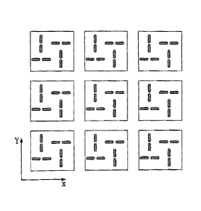
[054] Accordingly, with added reference to Figure 11 in conjunction with
Figure 10, and in accorqance With an 'illustrative embodiment of the present
invention, configurations (a) through (f) presented in Figure 10 may be
utilised
to reduce alien crosstalk between adjaoent connectors. Namely, the panel
configuration of Figure 11 illustrates a two-dimensionally periodic
configuration (in X. and Y) of contact pairs that both reduces pair-to-pair
crosstalk within a same connector, but also between connectors through
perpendicularity and symmetry of parasitic signal emission between adjacent
balanced pairs both within and between connectors. As it will now be
apparent to a person skilled in the art, the use of other such configurations,
as
sampled from the examples illustrated in Figure 10, can lead to similar
results.
[0551 Though the advantages of such configurations have been discusseq
and illustrated as pertaining to connector assembly wire port configurations,
it
will now be apparent to a person skilled in'the art that such configurations
can
also be useful in the cfesign of other data transmission products such as =,
PCBs, cables, connector boards, and other items of the like.
[0561 While this invention has been described with reference to the
illustrative embodiments, this description is not intended to be construea to
a
limiting sense. Various modifications or combinations of the illustrative
embodiments, as well as.other embodiments of 1he invention, will be =apparent
to persons skilled in the art upon reference to the description. It is
therefore
intendeq that the described invention encompass any such modifications or
embodiments-