Note: Descriptions are shown in the official language in which they were submitted.
CA 02588308 2007-05-24
WO 2006/063061 PCT/US2005/044282
1
SPECIFICATION
Improved Circuitry For Portable Lighting Devices And Portable Rechar eq able
Electronic Devices
Field of the Invention
The field of the present invention relates to portable electronic devices,
including hand held portable lighting devices, such as flashlights, and their
circuitry.
Background of the Invention
Various hand held or portable lighting devices, including flashlight designs,
are known in the art. Flashlights typically include one or more dry cell
batteries
having positive and negative electrodes. In certain designs, the batteries are
arranged in series in a battery compartment of a barrel or housing that can be
used to hold the flashlight. An electrical circuit is frequently established
from a
battery electrode through conductive means which are electrically coupled with
an
electrode of a lamp bulb. After passing through the lamp bulb, the electric
circuit
continues through a second electrode of the lamp bulb in electrical contact
with
conductive means, which in turn are in electrical contact with the other
electrode
of a battery. Incandescent lamp bulbs include a bulb filament. Typically, the
circuit includes a switch to open or close the circuit. Actuation of the
switch to
close the electrical circuit enables current to pass through the lamp bulb and
through the filament, in the case of an incandescent lamp bulb, thereby
generating
light.
Traditional flashlights use a mechanical switch to "turn on" the flashlight.
This is achieved by mechanically connecting two contacts and allowing current
to
flow from the positive terminal of the batteries, through the lamp, and back
to the
negative terminal of the batteries. One of the disadvantages of a mechanical
switch is that they are prone to wear and tear as well as oxidation of the
elements
that physically make and break the circuit. Mechanical switches also do not
permit automated or regulated modes of activating and deactivating a
flashlight.
Another disadvantage of traditional flashlights is that when they are
switched on they instantly allow large amounts of current to flow from the
batteries
through the lamp filament, thereby stressing the filament. This surge of
current
occurs because the resistance of the lamp's filament is very low when the
filament
is cold.
CA 02588308 2007-05-24
WO 2006/063061 PCT/US2005/044282
2
Essentially a lamp filament is a piece of wire that initially acts as a short
circuit. The filament resistance builds as the filament heats until the point
where
light is emitted. Consequently, when the flashlight is initially turned on, a
significantly greater amount of current than the bulb is designed to handle
flows
through the lamp. Although the current surge during this transient stage
exceeds
the bulb's design limits, the duration of the transient stage is short enough
that
bulbs generally survive the current surge. Over time, however, this rush of
current
causes damage to the lamp by stressing the filament and ultimately failure of
the
lamp filament. Indeed, it is generally during this transient stage that a lamp
filament will ultimately fail.
Yet another disadvantage of traditional flashlights is that they are generally
powered with alkaline or dry cell batteries. Alkaline or dry cell batteries,
when
exhausted, are discarded and users have to buy new ones to replace the
depleted
ones. Replacing batteries is an inconvenience and an additional expense to a
flashlight user. Furthermore, alkaline or dry cell batteries are heavy,
thereby
adding to the overall weight of the flashlight.
Rechargeable lead-acid batteries were developed to replace alkaline and
dry batteries. These types of batteries have the advantages of being
rechargeable and dischargeable for repeated use. They are, however, relatively
large and must be refilled with liquid electrolyte after being used for a
period of
time. Due to their bulky size and weight, even heavier than alkaline/dry cell
batteries, rechargeable lead-acid batteries are usually used with wall-mounted
safety lighting fixtures, motorcycles, and automobiles, but are generally not
considered suitable for use with portable lighting devices, such as
flashlights.
Nickel-cadmium batteries and nickel-metal hydride batteries have been
used to replace conventional batteries in flashlights. Nickel-cadmium and
nickel-
metal hydride batteries have the advantages of being light in weight,
convenient
for use, and repeatedly rechargeable and dischargeable. However, these
batteries have a disadvantage of causing heavy metal pollution. Moreover, the
nickel-cadmium and nickel-metal hydride batteries have the so-called battery
memory effect. Thus, in order to avoid shortening the life of the batteries,
it is
necessary to discharge any unused power of these types of batteries before
they
can be recharged.
An improved rechargeable energy source for portable electronic devices is
the lithium-ion battery. Lithium-ion batteries have a higher energy density
and a
lower self-discharge rate than nickel-cadmium and nickel-metal hydride
batteries.
Lithium-ion batteries also have a higher energy to weight ratio than nickel-
CA 02588308 2007-05-24
WO 2006/063061 PCT/US2005/044282
3
cadmium and nickel-metal hydride batteries. However, a lithium-ion battery can
explode if it is charged beyond its safe limits, or if its terminals are
shorted
together. Further, over discharging a lithium-ion battery can permanently
damage
the lithium-ion cell. Accordingly, most lithium-ion batteries are made
available in a
battery pack that includes a built-in protection circuit that has over charge,
over
discharge, and short circuit protection capabilities. This battery pack
protection
circuit internally blocks current from flowing from the lithium-ion battery
pack when
a short is detected. Thus, if there is a short across the recharging contacts
for the
device, the battery pack protection circuit trips and the electronic device
will cease
to operate
To avoid such inadvertent interruptions, recharging contacts of portable
electronic devices that are powered by a rechargeable lithium-ion batty pack
have
the contacts in hard to reach or hidden locations. Unfortunately, such a
configuration requires the use of plugs, special inserts, alignment tabs or a
complex cradle to recharge the batteries. Obstructing access to the recharging
contacts is not, however, a viable solution in the case of flashlights or
other
rechargeable devices where design requirements dictate that the charging
contacts or rings be exposed.
If rechargeable lithium-ion batteries were used in a flashlight with exposed
charge rings and the user accidentally created a short across the exposed
charge
contacts with a metal object such as his or her car keys, the lamp would go
off
until the metal object creating the short circuit is removed. Such inadvertent
interruptions may be dangerous when a user is working in an unlit area,
especially
for law enforcement and emergency response personnel. And, while a simple
diode can be placed in the recharging circuit to prevent accidental short
circuits
from being created across the charging rings or contacts for other
rechargeable
battery chemistries, such as nickel-cadmium and nickel metal hydride, this
solution is not viable for lithium-ion battery packs. A simple diode cannot be
used
in these circumstances because the forward voltage drop of a diode varies
greatly
while charging lithium-ion batteries requires very tight control over the
termination
voltage.
In view of the foregoing, rechargeable lithium-ion battery technology has
not been adopted for use in portable electronic devices with exposed charging
contacts, such as rechargeable flashlights. A need, therefore, exists for a
means
of providing improved short circuit protection in rechargeable devices, such
as
flashlights, having exposed charging contacts. A separate need also exists for
a
CA 02588308 2007-05-24
WO 2006/063061 PCT/US2005/044282
4
flashlight with improved circuitry that ameliorates one or more of the
problems
discussed above.
Summary Of The Invention
It is an object of the present invention to address or at least ameliorate one
or more of the problems associated with the flashlights and/or rechargeable
devices noted above.
Accordingly, in a first aspect of the invention, a portable rechargeable
electronic device, such as a flashlight, with external charging contacts and a
short
protection circuit is provided. The short protection circuit electrically
uncouples
one of the exposed charging contacts from the rechargeable power supply for
the
device when the charging contacts are shorted together. The charging contact
is
uncoupled without opening the power circuit for the device; thus, the device
can
continue to operate while the charging contacts are shorted. The power supply
for
the device may be a rechargeable lithium-ion battery pack.
According to one embodiment, the rechargeable electronic device
comprises a main power circuit including a DC power source and a power
consuming load, a first charging contact electrically coupled to a first
electrode of
the power source via a first electrical path, a second charging contact
electrically
coupled to a second electrode of the power source via a second electrical
path,
and a short protection circuit configured to open the first electrical path at
a
location that is not within the main power circuit if the first charging
contact and
the second charging contact are shorted together.
The short protection circuit preferably includes a switch interposed in the
first electrical path between the first charging contact and the first
electrode at a
location that is not within the main power circuit. The short protection
circuit may
be configured to open the switch if the first and second charging contacts are
shorted together. The switch may, for example, be a transistor, including
either a
field effect transistor or a bipolar transistor. Preferably the switch is a p-
channel
metal-oxide-semiconductor field effect transistor (MOSFET).
The short protection circuit may also include a comparing device adapted
to compare a voltage of a first input signal to a voltage of a second input
signal
and open or close the switch based on the comparison. The voltage of the first
signal may be proportional to the voltage difference between the first
charging
contact and ground and the voltage of the second signal may be proportional to
the voltage of the power source. The comparing device may, for example,
comprise a comparator, an op amp, an ASIC, or a processor. When the voltage
CA 02588308 2007-05-24
WO 2006/063061 PCT/US2005/044282
drop between the first charging contact and ground is approximately equal to
or
greater than the voltage of the battery, the switch is commanded to be in the
"on"
position by the comparing device. As a result, when the device is in its
charger
energy may flow from the charging contact to the power source. When the
5 voltage drop between the first charging contact and ground is zero, the
switch is
commanded to be in the "off' position. Thus, if a short occurs between the
charging contacts, the switch will be turned "off' or opened. As a result, the
power
source avoids any short across the charging contacts and can continue to
supply
power to the power consuming load.
The rechargeable device may comprise a flashlight, and the DC power
source may comprise a rechargeable lithium-ion battery pack. In case of a
short
across the charging contacts, the short protection circuit may be configured
to
detect and clear the short faster than the built-in short circuit protection
of the
lithium-ion battery pack. As such, the short protection circuit ensures that
the
operation of the device is not interrupted if a short occurs on the external
charging
contacts. This is particularly advantageous if the rechargeable device
comprises
a flashlight.
In yet a further embodiment, a rechargeable flashlight is provided that
comprises a power source, a lamp electrically coupled to the power source
through a main power circuit, a first charging contact electrically coupled to
a first
electrode of the power source through a first electrical path, a second
charging
contact electrically coupled to a second electrode of the power source through
a
second electrical path, and a logic circuit controlling a switch interposed in
the first
electrical path at a location that is not within the main power circuit. The
logic
circuit is configured to signal the switch to open if the first and second
charging
contacts are shorted together.
According to a second aspect of the invention, a portable lighting device
that includes a circuit for regulating current flow through the lamp of the
device is
provided. The circuit preferably reduces the initial surge of current that is
sent
through the lamp when the lamp is turned on. In the case of lighting devices
that
employ incandescent lamp bulbs, such a circuit may be used to reduce the
stresses placed on the lamp bulb when the lighting device is turned on,
thereby
extending the life expectancy of the lamp bulb.
According to one embodiment, the lighting device comprises a main power
circuit including a power source, a light source, and an electronic power
switch,
and a power control circuit. The power control circuit is electrically coupled
to the
electronic power switch and adapted to regulate current flow through the
CA 02588308 2007-05-24
WO 2006/063061 PCT/US2005/044282
6
electronic power switch in response to a control signal. The power control
circuit
may regulate the electronic power switch when the lighting device is turned on
to
limit the peak current that flows through the main power circuit prior to the
main
power circuit reaching a steady state. The electronic power switch may
comprise
a transistor, and the light source may include a filament. Preferably the
electronic
power switch comprises an n-channel MOSFET and the power control circuit
applies. the modified control signal to the gate of the MOSFET. The lighting
device may comprise a flashlight.
In a preferred embodiment, the lighting device further comprises a
microprocessor and a mechanical switch for opening and closing an electrical
path between the power source and the microprocessor. The microprocessor
provides the control signal to the power control circuit in response to an
activation
signal received from the mechanical switch, and the power control circuit
modifies
the control signal and applies the modified control signal to the electronic
power
switch. The voltage of the control signal may vary according to a step
function
when the lighting device is turned on, while the modified control signal may
have a
voltage that increases over time after the lighting device is turned on.
Preferably
the voltage of the modified control signal increases exponentially after the
flashlight is turned on.
According to another embodiment, the lighting device comprises a
flashlight having a main power circuit that includes a power source, a lamp,
and
an electronic power switch, and a power control circuit electrically coupled
to the
electronic power switch and adapted to provide a signal to the electronic
power
switch while the flashlight is on. In the present embodiment, the amount of
current
the electronic power switch is capable of conducting in the main power circuit
is
dependent on the voltage of the signal applied to the electronic power switch,
and
the power control circuit is configured to vary the voltage of the signal in a
manner
that increases the amount of current that can flow through the power switch
over a
predetermined period when the flashlight is turned on.
Preferably the predetermined period is set to be greater than the time
required for the main power circuit to reach a steady state after the
flashlight is
turned on. If the lamp includes a filament, the predetermined period is
preferably
greater than the thermal time constant of the filament. Typically, the
predetermined period will be 10 milliseconds or more, and more preferably the
predetermined period will be 40 milliseconds or more.
In one implementation, the power control circuit varies the voltage of the
signal according to an exponential function, preferably an increasing
exponential
CA 02588308 2007-05-24
WO 2006/063061 PCT/US2005/044282
7
function. Preferably the time constant of the exponential function is
determined by
the values of a resistor and a capacitor included in the power control
circuit.
The electronic power switch may comprise a transistor, such as a field
effect transistor or a bipolar transistor. Preferably, the electronic power
switch
comprises a MOSFET. If the electronic power switch comprises a field effect
transistor, the signal is applied to the gate of the transistor.
The flashlight may further comprise a microprocessor and a mechanical
switch for opening and closing an electrical path between the power source and
the microprocessor. The microprocessor provides a control signal to the power
control circuit in response to an activation signal received from the
mechanical
switch, and the power control circuit modifies the control signal to produce
the
signal applied to the electronic power switch. The voltage of the control
signal
preferably varies according to a step function when the flashlight is turned
on,
while the signal applied to the electronic power switch preferably increases
over
time according to an exponential function.
In another separate aspect of the present invention it is contemplated that
elements of the aforementioned aspects of the present invention may be
combined.
Further aspects, objects, desirable features, and advantages of the
invention will be better understood from the following description considered
in
connection with accompanying drawings in which various embodiments of the
disclosed invention are illustrated by way of example. It is to be expressly
understood, however, that the drawings are for the purpose of illustration
only and
are not intended as a definition of the limits of the invention.
Brief Description Of The Drawings
FIG. 1 is a perspective view of a flashlight according to one embodiment of
the present invention.
FIG. 2 is a cross-sectional view of the flashlight of FIG. 1 taken through the
plane indicated by 2-2.
FIG. 3 is an enlarged cross-sectional view of the forward section of the
flashlight of FIG. 1 taken through the plane indicated by 2-2.
FIG. 4 is a perspective view of the cross-sectional view shown in FIG. 3.
FIG. 5 is a circuit diagram for the flashlight of FIG. 1 illustrating the
relationship of the electronic circuitry according to one embodiment of the
invention.
CA 02588308 2007-05-24
WO 2006/063061 PCT/US2005/044282
8
FIG. 6 is a circuit diagram of one embodiment of a debounce circuit for a
momentary switch that may be employed in a flashlight according to the present
invention.
FIG. 7 is a circuit diagram of one embodiment of a microcontroller that may
be employed in a flashlight according to present invention.
FIG. 8 is a circuit diagram of one embodiment of a power control circuit that
may be employed in a flashlight according to the present invention.
FIG. 9A is a circuit diagram of one embodiment of a short prevention circuit
according to the present invention.
FIG. 9B is a circuit diagram of one example of a power supply circuit for a
comparing device employed in short prevention circuit of FIG. 9A.
FIG. 10A shows three oscilloscope traces reflecting (1) how the voltage of
a control signal from the microcontroller of the flashlight shown in FIG. 1
may vary
over time when the flashlight is initially turned on, (2) how the voltage of a
signal
from the power control circuit varies in response to the control signal of the
microcontroller, and (3) how the current supplied to the lamp of the
flashlight
varies in response to the signal from the power control circuit.
FIG. 10B shows three oscilloscope traces for a flashlight without a power
control circuit according to the present invention, but was otherwise the same
as
the flashlight used to obtain the oscilloscope traces shown in FIG. 10A. The
three
traces shown in FIG. 10B reflect (1) how the voltage of a control signal from
a
microcontroller of a flashlight without a power control circuit may vary over
time
when the flashlight is initially turned on, (2) how the gate-to-source voltage
of the
electronic power switch will vary in response to the voltage of the control
signal,
and (3) how the current supplied to the lamp of the flashlight varies in
response to
the voltage applied to the electronic power switch.
FIG. 1 1A is an oscilloscope trace showing current flow over time in the
main power circuit of a flashlight equipped with a power control circuit
according to
the present invention when the flashlight is initially turned on.
FIG. 11 B is an oscilloscope trace showing current flow over time in the
main power circuit of a flashlight without a power control circuit according
to the
present invention when the flashlight is initially turned on.
FIG. 12 shows three oscilloscope traces for a flashlight according to the
present invention that was operated in a strobe mode. The three traces
reflect:
(1) the voltage of the control signal from the microprocessor, (2) the voltage
of the
modified control signal generated by the power control circuit, and (3) the
current
flow through the electronic power switch.
CA 02588308 2007-05-24
WO 2006/063061 PCT/US2005/044282
9
FIG. 13 shows three oscilloscope traces for a flashlight according to the
present invention that was operated in a power reduction mode. The three
traces
reflect: (1) the voltage of the control signal from the microprocessor, (2)
the
voltage of the modified control signal generated by the power control circuit,
and
(3) the current flow through the electronic power switch.
Detailed Description Of Preferred Embodiments
To facilitate the description of the invention, any reference numeral
representing an element in one figure will represent the same element in any
other figure.
A flashlight 10 according to one embodiment of the present invention is
illustrated in perspective in FIG. 1. The flashlight 10 incorporates a number
of
distinct aspects of the present invention. While these distinct aspects have
all
been incorporated into the flashlight 10, it is to be expressly understood
that the
present invention is not restricted to flashlight 10 described herein. Rather,
the
present invention is directed to each of the inventive features of the
flashlight
described below individually as well as collectively. Further, as will become
apparent to those skilled in the art after reviewing the present disclosure,
one or
more aspects of the present invention may also be incorporated into other
electronic devices, including cell phones, portable radios, toys, as well as
other
non-portable lighting devices.
Referring to FIGS. 1-4, flashlight 10 includes a barrel 21 enclosed at a
rearward end by a tail cap 22 and at a forward end by a head and switch
assembly 23.
Barrel 21 is preferably made out of aluminum. As is known in the art, barrel
21 may be provided with a textured surface 27 along its axial extent,
preferably in
the form of machined knurling.
In the present embodiment, barrel 21 is configured to enclose a
rechargeable lithium-ion battery pack 60. Battery pack 60 may comprise one or
more lithium-ion battery cells. Preferably battery pack 60 comprises at least
two
lithium-ion cells disposed physically in a series or end to end arrangement,
while
being electrically connected in parallel. In other embodiments, it may be
desirable
to electrically connect the two cells in series. Further, barrel 21 may also
be
configured to include a battery pack 60 comprising two or more lithium-ion
batteries or cells physically disposed in a parallel or side-by-side
arrangement,
while being electrically connected in series or parallel depending on the
design
requirements of the flashlight. Furthermore, while a lithium-ion battery pack
60 is
CA 02588308 2007-05-24
WO 2006/063061 PCT/US2005/044282
used as the power source for the illustrated embodiment of flashlight 10, in
other
embodiments of the present invention, other DC power sources may be
employed, including, for example, dry cell batteries as well as other types of
rechargeable batteries.
5 The rechargeable lithium-ion battery pack 60 preferably includes built-in
short circuit protection circuitry 86, as best seen in FIG. 5. Battery packs
of this
type are readily available in the market from such providers as BYD Company
Limited and will interrupt the flow of current from the battery pack if the
electrodes
of the battery back are shorted together.
10 Tail cap 22 is also preferably made out of aluminum and is configured to
engage mating threads provided on the interior of barrel 21 as is conventional
in
the art. However, other suitable means may also be employed for attaching tail
cap 22 to barrel 21. As best seen in FIG. 2, a one-way valve 68, such as a lip
seal, may be provided at the interface between the tail cap 22 and barrel 21
to
provide a watertight seal. However, as those skilled in the art will
appreciate,
other forms of sealing elements, such as an 0-ring, may be used instead of one-
way valve 68 to form a watertight seal. One way valve 68 is retained in a
circumferential channel 70 formed in tail cap 22. Further one-way valve 68 is
oriented so as to prevent flow from outside into the interior of the
flashlight 10,
while simultaneously allowing overpressure within the flashlight to escape or
vent
to atmosphere.
The design and use of one-way valves in flashlights is more fully described
in U.S. Patent No. 5,113,326 to Anthony Maglica, which is hereby incorporated
by
reference.
If made out of aluminum, the surfaces of barrel 21 and tail cap 22 are
preferably anodized with the exception of those surfaces used to make
electrical
contact with another metal surface for purposes of forming the electrical
circuit of
the flashlight. In the present embodiment, an electrical path is formed
between
barrel 21 and the case electrode 61 of the lithium-ion battery pack 60 by
conductive member 72 and spring 74. In addition to forming part of the
electrical
path between the barrel and case electrode, spring 74 also urges battery pack
60
forward so that the center electrode 63 of battery pack 60 is urged into one
end of
spring biased conductor 76, which is held by and extends through retaining
bolt
57.
The head and switch assembly 23 of the present embodiment includes a
support structure 28 to which a number of other components may be mounted,
including, for example, head 24, face cap 25, charging contact 44, printed
circuit
CA 02588308 2007-05-24
WO 2006/063061 PCT/US2005/044282
11
board 46, sleeve 50, switch 52, and moveable lamp assembly 100. For ease of
manufacturing, support structure 28 is preferably made out of injection molded
plastic. Head 24, face cap 25, and sleeve 50, on the other hand, are
preferably
made from anodized aluminum.
In the present embodiment, support structure 28 is a hollow support
structure comprising a front section 31, a midsection 33 and an aft section
35.
The front section 31 comprises a generally cup-shaped receiving area 37. The
midsection 33, which extends rearward from the front section 31, includes a
generally cylindrical inner surface 39. And, the aft section 35, which extends
rearward from the midsection 33, includes two opposing arcuate threaded
fingers
55 (only one of which is visible in the cross-sections of FIGS. 2-4).
The face cap 25 retains lens 26 and reflector 30 relative to the support
structure 28. In the present embodiment face cap 25 is configured to thread
onto
external threads 29 provided on the front section 31 of the support structure
28.
In other implementations, however, other forms of attachment may be adopted.
As illustrated, reflector 30 is positioned within the cup-shaped receiving
area 37 of
the front section 31 of support structure 28. Corresponding alignment features
32,
34 may be provided on the outer surface of reflector 30 and the internal
mating
surface of support structure 28, respectively, to ensure proper alignment
between
the reflector 30 and support structure 28.
Head 24 has a diameter greater than that of the barrel 21 and sleeve 50.
Head 24 is also adapted to pass externally over the exterior of the barrel 21
and
sleeve 50. Internal surface 36 of head 24 is configured to mate with the outer
surface 38 of support structure 28 at select locations to properly position
head 24
relative to face cap 25 and support structure 28. A compressible retaining
ring 40,
such as a rubber 0-ring, may be seated in a channel 41 extending around the
outer surface 38 of support structure 28 to create an interference fit between
the
support structure 28 and a feature provided on the internal surface 36 of head
24,
such as circumferential lip 42. Compressible retaining ring 40 also prevents
moisture and dirt from entering the head assembly between the support
structure
28 and forward end of head 24.
External charging contacts 44 and 48 are provided at the forward section of
flashlight 10. While charging contacts 44 and 48 are provided in the present
embodiment in the form of charging rings to simplify the recharging procedure,
in
other embodiments contacts 44 and 48 may take on other forms. In the present
embodiment, printed circuit board 46 is interposed between charging contacts
44
and 48. Printed circuit board 46 is configured to be in electrical
communication
CA 02588308 2007-05-24
WO 2006/063061 PCT/US2005/044282
12
with charging contacts 44 and 48, while simultaneously isolating charging
contacts
44, 48 from direct electrical communication with one another through a short
circuit. Electrical communication between printed circuit board 46 and
charging
contacts 44, 48 may be established by providing a conductive trace at the
interface formed between printed circuit board 46 and each of the charging
contacts.
External charging contact 44 is preferably an aluminum ring disposed on
the external surface 38 of support structure 28, preferably toward the aft end
of
the mid-section 33. If barrel 21 is made out of anodized aluminum, external
charging contact 48 may be integrally formed in barrel 21 by machining a
portion
of the barrel to remove any anodizing from the location of charging contact 48
or
by masking the location of charging contact 48 prior to anodizing the barrel
21. In
the present embodiment, charging contact 48 is located at the forward end of
barrel 21.
As noted above, the head and switch assembly 23 also preferably includes
a sleeve 50. Sleeve 50 is disposed over the external surface 38 of the support
structure 28 so that it extends forward frorri the charging contact 44 to a
position
that is under the trailing edge 53 of head 24. Sleeve 50 is preferably made
out of
anodized aluminum, but may also be made out of other metals or plastics. As a
result of the foregoing construction, with the exception of the external
surface
formed by printed circuit board 48 and switch 52, all of the external surfaces
of the
flashlight 10 according to the present embodiment may be made out of metal,
and
more preferably aluminum.
Sleeve 50 is provided with a hole 51 through which switch cover 54 of
switch 52 extends. The outer surface of sleeve 50 surrounding switch cover 54
may be beveled to facilitate tactile operation of flashlight 10. Sleeve 50 may
also
be provided with a groove 56 about its circumference at a location forward of
the
trailing edge 53 of head 24 for positioning a sealing element 58, such as an 0-
ring, to form a watertight seal between the head 24 and sleeve 50. Similarly,
switch cover 54 is preferably made from molded rubber or latex. As best
illustrated in FIGS. 3 and 4, switch cover 54 is preferably configured to
prevent
moisture and dirt from entering the head and switch assembly 23 through hole
51.
In the present embodiment, lamp 59 is removeably mounted within the
head and switch assembly 23 so as to extend into reflector 30 through a
central
hole provided therein. In particular, lamp 59 is mounted on moveable lamp
assembly 100, which in turn is slideably mounted within the mid-section 33 of
support structure 28.
CA 02588308 2007-05-24
WO 2006/063061 PCT/US2005/044282
13
While lamp 59 may be any suitable device that generates light, in the
present embodiment lamp 59 is preferably an incandescent lamp bulb, and more
preferably a bi-pin incandescent lamp bulb. In other implementations of the
invention, however, lamp 59 may comprise, for example, an LED lamp or an arc
lamp.
In the present embodiment, moveable lamp assembly 100 includes an
adjustable ball housing 102, a ball-shaped adjustable bulb holder 104, an end
cap
106, a retainer 108, retention spring 110, a spring biased conductor 112,
spring
114, conductor post 116 and cam follower assembly 117.
As seen in FIGS. 3 and 4, lamp 59 is held by the ball-shaped adjustable
bulb holder 104. The ball-shaped adjustable bulb holder 104 is in turn
adjustably
mounted within adjustable ball housing 102. In this regard, adjustable ball
housing 102 is partially enclosed at its forward end by wall 103. Wall 103
includes
a concave mating surface 118 against which ball-shaped bulb holder 104 is
adjustably retained. Retainer 108, which is adapted to slide within adjustable
ball
housing 102, includes a concave surface 120 designed to slideably mate with
the
opposite side of ball-shaped adjustable bulb holder 104. End cap 106 encloses
the aft end of adjustable ball housing 102 and is mounted in a fixed
relationship
thereto. Retention spring 104 is interposed between the fixed end cap 106 and
the slideable retainer 108, thereby biasing retainer 108 toward the forward
end of
the flashlight until concave surface 120 engages ball-shaped adjustable bulb
holder 104. As a result, ball-shaped adjustable bulb holder 104 is adjustably
held
between concave surface 118 of wall 103 and concave surface 120 of retainer
108.
Ball-shaped adjustable bulb holder 104 includes a metal portion 122, a first
contact holder 124, and a second contact holder 126. In the present
embodiment,
the metal portion 122 comprises a zone of a sphere with a through hole. First
contact holder 124 and second contact holder 126 are made from a non-
conductive material, such as plastic, and are configured to create an
interference
fit within the through hole of metal portion 122. The second contact holder
126
includes a head portion shaped like a sector of a sphere so that in
combination
with the metal portion 122 the ball-shaped adjustable bulb holder 104 is
provided
with a substantially spherical outer surface.
The electrodes of lamp 59 extend into the first contact holder 122 where
they preferably frictionally engage with positive and negative electrode
contacts,
respectively (not shown). One of the electrode contacts, the negative in the
present embodiment, is configured to extend between the mating surfaces of the
CA 02588308 2007-05-24
WO 2006/063061 PCT/US2005/044282
14
first and second contact holders 124, 126 and make electrical connection with
the
metal portion 122 of ball-shaped adjustable bulb holder 104. The other
electrode
contact, the positive in the present embodiment, extends through both the
first and
second contact holders 124, 126 and includes a surface for mating with the
spring
biased conductor 112.
The construction of moveable lamp assembly 100 is described in detail in
connection with FIGS. 6-18 of pending U.S. Patent Application Serial No.
10/802,265, filed March 16, 2004, which is hereby incorporated by reference.
The metal portion 122 of ball-shaped adjustable bulb holder 104 is in
electrical communication with adjustable ball housing 102, which is also
preferably
made out of metal. Adjustable ball housing 102 is in turn in electrical
communication with leaf spring conductor 128, a portion of which is in
slideable
contact with the exterior of adjustable ball housing 102. Leaf spring
conductor
128 is also in electrical communication with printed circuit board 46 at
contact pad
62 on printed circuit board 46.
Contact post 116 extends through end cap 106 and switch housing 80.
Contact post 116 is frictionally held by switch housing 80 so that its aft end
is in
electrical communication with printed circuit board 46 at via 64. Via 64
extends
through the center of printed circuit board 46 in the present embodiment. At
its
forward end, contact post 116 is slideably supported within the through hole
provided in end cap 106. A cup-shaped portion 130 provided on the forward end
of contact post 116 is configured to hold one end of spring 114 while the
other end
of spring 114 forces spring biased conductor 112 into contact with an exposed
portion of the electrode contact extending through the second contact holder
126
of ball-shaped adjustable bulb holder 104. Spring biased conductor 112 is also
cup-shaped in the present embodiment and has a diameter slightly greater than
that of cup-shaped portion 130 so that it can slideably fit over the exterior
surface
of the cup-shaped portion 130 and hold spring 114 therebetween.
The head and switch assembly 23 is attached to barrel 21 by way of the
two arcuate threaded fingers 55 forming the aft section 35 of support
structure 28.
The two arcuate threaded fingers 55 extend through printed circuit board 46.
The
arcuate threaded fingers 55 are provided with both external and internal
threads.
The external threads mate with corresponding internal threads provided within
the
forward end of barrel 21. Once the head and switch assembly 23 is threaded
into
the barrel 21, retaining bolt 57 is threaded into the internal threads of the
arcuate
threaded fingers 55. Preferably the retaining bolt 57 includes a tapered shaft
59
CA 02588308 2007-05-24
WO 2006/063061 PCT/US2005/044282
configured to spread the arcuate threaded fingers 55, thereby locking the head
and switch assembly 23 to the barrel.
Spring biased conductor 76 is compressibly held within central cavity 66 of
retaining bolt 57 between printed circuit board 46 and end wall 67. Spring
biased
5 conductor 76 also electrically couples via 64 on printed circuit board 46 to
center
electrode 63 of rechargeable lithium-ion battery pack 60.
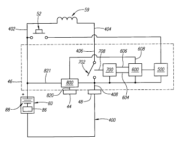
FIG. 5 is a circuit diagram for flashlight 10 and schematically represents a
preferred embodiment of the electronic circuitry according to the present
invention. As shown in FIG. 5, flashlight 10 includes a main power circuit
400, a
10 switch 52, a debounce circuit 500, a microprocessor control circuit 600, a
power
control circuit 700, charging contacts 44, 48, and a short protection circuit
800. In
the present embodiment, debounce circuit 500, microprocessor control circuit
600,
power control circuit 700, and short protection circuit 800 are all formed on
printed
circuit board 46. In other implementations, however, other arrangements are
15 possible.
Main power circuit 400 of the present embodiment comprises, rechargeable
lithium-ion battery pack 60, electrical path 402, lamp 59, electrical path
404, and
electronic power switch 702.
As best seen in FIG. 5, rechargeable lithium-ion battery pack 60 includes
built in short circuit protection circuitry 86. The built in short circuit
protection
circuitry 86 is disposed in series with lithium-ion cell 88 within lithium-ion
battery
pack 60. In the illustrated embodiment, the short circuit protection circuitry
is
disposed between the negative electrode of lithium-ion cell 88 and the
negative
electrode of battery pack 60. Built-in short circuit protection circuitry 86
could,
however, also be provided between the positive electrode of lithium-ion cell
88
and the positive electrode of battery pack 60.
Electrical path 402 connects the center electrode 63 of rechargeable
lithium-ion battery pack 60 to the positive electrode of lamp 59. In the
flashlight
illustrated in FIGS. 1-4, electrical path 402 comprises the following
elements:
spring biased conductor 76, via 64, conductor post 116, spring 114, spring
biased
conductor 112, and the positive electrode contact disposed within ball-shaped
adjustable bulb holder 104.
Electrical path 402 connects the negative electrode of lamp 59 to the case
electrode 61 of the rechargeable lithium-ion battery pack. Further, electrical
path
404 is opened and closed to complete and break the main power circuit 400 by
electronic power switch 702, which is described in more detail below. In the
flashlight illustrated in FIGS. 1-4, electrical path 404 comprises: the
negative
CA 02588308 2007-05-24
WO 2006/063061 PCT/US2005/044282
16
electrode contact disposed within ball-shaped adjustable bulb holder 104, the
metal portion 122 of ball-shaped adjustable bulb holder 104, adjustable ball
housing 102, leaf spring conductor 128, contact pad 62, conductive trace 406,
electronic power switch 702, conductive trace 408, barrel 21, conductive
member
72 in tail cap 22, and spring 74.
While electronic power switch 702 is located on printed circuit board 46 in
the present embodiment, electronic power switch 702 may also be located in
other
places within flashlight 10.
Electronic power switch 702 is electrically coupled to contact pad 62 via
conductive trace 406, which is also provided on printed circuit board 46.
Electronic power switch 702 is also electrically coupled to barrel 21 via
conductive
trace 408, which extends on printed circuit board 46 from electronic power
switch
702 to the interface between printed circuit board 46 and barrel 21.
It is noted that other than electronic power switch 702, the constituent
members of electrical paths 402, 404 are not critical to the operation of
power
circuit 400 according to the present aspect of the invention and any
combination
of members as may be appropriate for forming the electrical paths of a power
circuit for a particular flashlight design may be employed.
Electronic power switch 702 selectively opens and closes the electrical
path 404 between the lamp 59 and case electrode 61 of the rechargeable lithium-
ion battery pack 60. When electronic power switch 702 is closed, current is
permitted to flow through main power circuit 400.
The opening and closing of electronic power switch 702 is controlled, in the
present embodiment, by switch 52, microcontroller circuit 600 and power
control
circuit 700.
Manipulation of switch 52 generates a signal which determines whether
electronic power switch 702 opens or closes, or repeatedly opens and closes in
a
manner hereinafter described.
In the present embodiment, switch 52 is a momentary switch. When switch
52 is depressed, plunger 69 of switch 52 pushes snap dome 84 of conductor 82
into electrical communication with conductor post 116. A signal from battery
pack
60 is then transmitted to printed circuit board 46 through contact pad 65.
When
this signal is transmitted to printed circuit board 46, electronic power
switch 702
may be signaled to open or close the electrical path 404, thereby permitting
flashlight 10 to be turned on or off accordingly.
Unlike mechanical switches known in the art, switch 52 does not conduct
current to the lamp 59. Instead, switch 52 merely provides an activation or
CA 02588308 2007-05-24
WO 2006/063061 PCT/US2005/044282
17
deactivation signal. In the present embodiment, this activation or
deactivation
signal is sent to microcontroller circuit 600, which in turn signals
electronic power
switch 702 through power control circuit 700 to open or close accordingly. The
main power circuit 400 in the present embodiment is thus indirectly activated
or
deactivated by the manipulation of switch 52 by a user.
Because the current from rechargeable lithium-ion battery pack 60 to the
lamp 59 passes through electronic power switch 702, and not switch 52, switch
52
may be designed to operate under very low current.
In the illustrated embodiment shown in FIG. 5, switch 52, debounce circuit
500, microcontroller circuit 600, power control circuit 700, and electronic
power
switch 702 are all in electrical communication. When switch 52 is initially
depressed, a signal is sent to the microcontroller circuit 600 through the
debounce
circuit 500. The microcontroller circuit 600 in response sends a signal
through the
power control circuit 700 to the electronic power switch 702. In response, the
electronic power switch 702 permits current to flow to lamp 59 from the
lithium-ion
battery pack 60 at a controlled increasing rate over a predetermined period. A
more detailed description of debounce circuit 500, microcontroller circuit
600,
power control circuit 700, and electronic power switch 702 are discussed below
in
connection with FIGS. 6, 7, and 8.
FIG. 6 is a detailed schematic of one embodiment of a debounce circuit
500 that may be employed in the present invention. Debounce circuit 500 may be
used to reduce the noise, current, and voltage of the signal sent from switch
52 to
the microcontroller circuit 600.
A signal to turn lamp 59 on or off enters the debounce circuit 500 through
contact pad 65 when a user manipulates switch 52 in a manner so as to cause
plunger 69 to force snap dome 84 into contact with conductor post 116. As a
result of this manipulation, a signal is sent via contact pad 65 through
debounce
circuit 500. The output of the debounce circuit 500 is provided at output 507,
which is in electrical communication with microcontroller circuit 600
illustrated in
FIG. 7.
In one embodiment of debounce circuit 500, capacitors 502, 504, 505, and
resistor 503 are coupled in parallel to contact pad 65 and output 507, while
resistor 506 is serially interposed between contact pad 65 and output 57,
preferably down stream of the parallel branches for capacitor 502 and resistor
503.
Those skilled in the art will know how to design a debounce circuit 500 to
achieve a suitable signal level to microcontroller circuit 600. In the design
CA 02588308 2007-05-24
WO 2006/063061 PCT/US2005/044282
18
illustrated in FIG. 6, however, it has been found that resistor 506 may have a
resistance of 10 KQ, resistor 503 may have a resistance of 1 KO, and
capacitors
502, 504, and 505 may each have a capacitance of 0.1 pF.
FIG. 7 is a schematic diagram of microcontroller circuit 600. In the present
embodiment, microcontroller circuit 600 includes a microcontroller 601 having
an
input 602 and two outputs 604, 606. Further, the GND pin of microcontroller
601
is directly connected to ground, and the Vcc pin of the microcontroller 601 is
electrically connected to battery pack 60 via conductive trace 608 and to
ground
through capacitor 610 via conductive trace 612. The signal provided on trace
608
may also be a battery signal that has been filtered by a diode, although such
filtering is unnecessary. If such filtering is performed, it may be performed
in the
short protection circuit 800 as described below.
A signal from output 507 of the debounce circuit 500 enters microcontroller
601 through input pin 602. Microcontroller 601 may be programmed to provide
for
different user selectable functions, the selection of which may be controlled
by the
nature of the input signal received on input pin 602. Thus, for example, if
flashlight 10 is in the off state and switch 52 is depressed and released,
microcontroller 601 may be programmed to provide a signal on output pin 606
that
will turn flashlight 10 on. Microcontroller 601 may further be programmed so
that
the flashlight 10 will stay on with a second depression of switch 52 until the
second release of switch 52. Other functions may also be programmed into
microcontroller 601. For example, microcontroller 601 may be programmed such
that a user may select a power reduction mode by depressing switch 52 and
holding it down for two seconds or a strobe mode by depressing switch 52 and
holding for 4 seconds.
If flashlight 10 is in the off state, microcontroller 601 will send a control
signal out through output pin 606 in response to a signal received through
input
pin 602. The control signal from output pin 606 is provided to input 707 of
power
control circuit 700 where it is modified in a desired manner before being
supplied
over trace 708 to electronic power switch 702 so that electronic power switch
702
is gradually closed in response to the control signal, thereby limiting the
initial in-
rush of current through lamp 59.
In connection with other operational modes programmed into
microcontroller 601, it may be desirable to modify the control signal produced
by
microcontroller 601 in an alternative manner. Accordingly, in the illustrated
embodiment, microcontroller 601 also includes a second output 604 for
providing
a second control signal to power control circuit 700. A control signal from
output
CA 02588308 2007-05-24
WO 2006/063061 PCT/US2005/044282
19
pin 604 is provided to input 709 of power control circuit 700. The control
signal
from output pin 604 is modified within power control circuit 700 before being
provided on trace 708 to electronic power switch 702 so that power switch 702
is
closed at a different rate in response to a control signal provided on output
pin 604
of microcontroller 601.
FIG. 7 is a schematic diagram of power control circuit 700, which is coupled
to electronic power switch 702 via conductive trace 708. An electronic power
switch 702 is selected that permits different levels of current to flow
through main
power circuit 400 in response to different signal levels provided at trace
708. In
the present embodiment, electronic power switch 702 comprises an n-channel
MOSFET 705. The gate of the MOSFET is electrically connected to trace 708,
the drain to the center electrode 63 of battery pack 60 through input 703, and
the
source to ground (e.g., the case electrode 61 of battery pack 60). An n-
channel
MOSFET works well in the present invention due to its transfer
characteristics,
namely that the drain current is zero (i.e., the electronic power switch 702
is open)
when the gate-to-source voltage is below approximately 0.75 Volts.
While the present embodiment employs an n-channel MOSFET 705, it will
become apparent to those skilled in the art from the present disclosure that
other
types of electronic power switches may also be employed in the present
invention.
For example, a p-channel MOSFET could be used in place of the n-channel
MOSFET if electronic power switch 702 were provided on the high-side of main
power circuit 400 (i.e., prior to lamp 59). Similarly, other types of
transistors may
also be employed for electronic power switch 702, including other field effect
transistors; such as JFETs and DE MOSFETs, and bipolar junction transistors.
As noted above, power control circuit 700 modifies the control signals
received from output pins 604, 606 of microcontroller 601. In particular,
power
control circuit 700 is designed to modify the control signals so that they
vary over
time based on the transfer characteristics of the employed electronic power
switch
702 and the rate at which electronic power switch 702 is to be closed.
Preferably,
power circuit 700 modifies at least one of the control signals received from
microcontroller 601 so that when the control signal reaches electronic power
switch 702, electronic power switch 702 is gradually closed over time, as
opposed
to being closed instantaneously.
When flashlight 10 is in the off state, the signals at inputs 707 and 709 are
both high impedance signals so they are effectively not part of power control
circuit 700. Further, the value of resistor 703 is selected so that when
flashlight 10
CA 02588308 2007-05-24
WO 2006/063061 PCT/US2005/044282
is in the off state, resistor 703 pulls the gate voltage of MOSFET 705 to zero
volts
(through resistor 701) so that electronic power switch 702 is open.
The degree to which electronic power switch 702 is closed and hence the
amount of current permitted to flow in main power circuit 400 is ultimately
5 controlled in the illustrated embodiment by the voltage across capacitor
710,
which also correspond to the gate-to-source voltage of MOSFET 705. When a
control signal is provided on inputs 707 or 709, the voltage across capacitor
710
will increase exponentially according to the equation V, = E(1-e"t/T) until
the
maximum voltage of the control signal is achieved. In the foregoing equation,
E is
10 the voltage of the control signal applied to input 707 or 709 and T is the
time
constant for the circuit and is determined by the equation T = RC. Further,
while it
takes a period of approximately 5T before a capacitor is fully charged, during
a
period of 1 T the voltage across capacitor 710 will reach approximately 63% of
the
voltage of the applied control signal from microcontroller 601. Thus, by
15 appropriately selecting R and C for each of the circuit paths corresponding
to
inputs 707 and 709, the rate at which the gate-to-source voltage increases,
and
hence how quickly the electronic power switch 702 is closed, after a control
signal
is provided from microcontroller 601, may be controlled.
As noted above, when flashlight 10 is initially turned on, a control signal is
20 provided from output pin 606 of microcontroller 601 to input 707 of power
control
circuit 700. As a result, the signal at input 707 goes from high impedance to,
for
example, a 3 Volt signal instantaneously. The voltage across capacitor 710,
and
hence the gate-to-source voltage will, however, increase exponentially to 3
Volts
according to the formula given above. By gradually increasing the voltage of
the
control signal to reach electronic power switch 702 over trace 708 in the
foregoing
manner, the current permitted to flow to lamp 59 may be increased at a
controlled
rate. In turn, by increasing the amount of current sent to lamp 59 at a
controlled
rate, lamp 59 may be permitted to achieve its steady state resistance at a
controlled, reduced rate, thereby protecting lamp 59 from the normal large
initial
surge of current from battery pack 60 when the flashlight is turned on.
In a preferred embodiment, resistor 701 has a resistance of 470 Kf2,
resistor 703 has a resistance of 1 KC) and capacitor 710 has a capacitance of
0.1
pF. This combination of resistor 701 and capacitor 703 forms a low pass filter
with a time constant of 47 ms (470,000 x 0.000001 = 0.047 seconds or 47
milliseconds). During this period capacitor 710 will be charged to
approximately
63% of the voltage of the control signal provided on input 707 (or 0.63 * 5
Volts =
3.15 Volts). This means that it will take approximately 47 ms for the gate-to-
CA 02588308 2007-05-24
WO 2006/063061 PCT/US2005/044282
21
source voltage of MOSFET 705 to pass from the off region, through the current
limited region, to the linear region of the transistor. During this time, the
filament
of lamp 59 is heated while limiting the in-rush of current to a more desirable
level.
As noted above, a control signal provided on output 604 of microcontroller
601 may be provided to input 709 for purposes of closing electronic power
switch
702 at a different rate than that achieved by a control signal provided at
input 707.
For example, resistor 704 may be set at 1.0 KO, while capacitor 710 is still
set at a
capacitance of 0.1 pF. This combination results in a low pass filter circuit
with a
time constant of 0.0001 seconds (0.1 ms). Thus, under this configuration,
capacitor 710 will be charged to approximately 63% of the voltage of the
control
signal provided at input 709 (or 3.15 Volts in the present embodiment) in 0.1
ms.
Accordingly, a control signal provided on input 709 of power control circuit
700 may be used to close and open electronic power switch 702 at much higher
frequency than a control signal provided on input 707. This feature may be
desirable for certain user selectable functions, such as a power reduction
mode.
For example, if a user selects a power reduction mode by depressing switch 52
for an appropriate duration, the microcontroller 601 may send out an initial
control
signal from output pin 606 to input 707 to energize lamp 59 relatively slowly
as
described above. After the lamp 59 has already been turned on and the filament
has been heated so that it is at or near its steady state resistance,
microcontroller
601 may send out a square wave pulse modulated control signal, such as the one
shown in FIG. 13, from output pin 604 to input 709 of power control circuit
700 and
stop sending out a control signal on output 606.
Based on a time constant of 0.1 ms, the pulse modulated signal sent out
from output pin 604 of microcontroller 601 could be modulated at a rate
between
approximately 5 kHz and 100 Hz, and still be at a frequency that is much
higher
than the visible flicker rate of 60 Hz. Further, due to the short cycle time
between
each pulse, the filament of lamp 59 will not cool sufficiently between cycles
so as
to result in undue stress by the high frequency of the on, off cycles. As a
result,
flashlight 10 may be operated in a manner that will permit lamp 59 to, for
example,
operate at half power and thus consume half the energy it would normally
consume over a given period of time.
Although the power control circuit of the present embodiment has been
described as employing an RC circuit to modify the control signal provided to
electronic power switch 702, other forms of circuits with time constants, such
as
RL and RLC circuits, may be employed in power control circuit 700 as well. In
addition, circuits that produce linear, sinusoidal, saw tooth, or triangular
CA 02588308 2007-05-24
WO 2006/063061 PCT/US2005/044282
22
waveforms may also be used for power control circuit 700. Further, the
benefits of
power control circuit 700 may be realized in a flashlight in which the control
signal
delivered to the power control circuit comes directly from a mechanical switch
as
opposed to a microcontroller or in which any form of DC power source is
substituted for battery pack 60.
FIGS. 10A graphically demonstrates the beneficial dampening effects that
power control circuit 700 may provide to lamp 59 when flashlight 10 is
initially
turned on. In contrast, FIG. 10B graphically demonstrates that the rate of
change
of current flow and the peak current flow through electronic power switch 702
is
much greater when a power control circuit 700 according to the present
invention
is not controlling the signal to electronic power switch 702.
FIG. 10A shows three oscilloscope traces 1002, 1004, 1006. The
oscilloscope traces of FIG. 10A were obtained from a flashlight having a power
control circuit 700 as described above in connection with FIG. 8 to drive an
electronic power switch 702 comprising a MOSFET 705. Further, the resistor 701
had a value of 470 KO and the capacitor 710 had a value of 0.1 pF. The time
constant for the power control circuit was thus 47 ms.
The oscilloscope traces of FIG. 10B were obtained at a time when the
flashlight went from the off state to the on state and respectively reflect
(1) how
the voltage of the control signal from the microcontroller 601 of the
flashlight
varied over time when the flashlight was initially turned on, (2) how the
voltage of
the signal from the power control circuit 700, and hence the gate-to-source
voltage of MOSFET 705, varied in response to the control signal of the
microcontroller, and (3) how the current that traveled through MOSFET 705, and
hence supplied to the lamp 59 of the flashlight, varied in response to the
signal
from the power control circuit.
The x-axis of FIG. 10A represents time in milliseconds, and the distance
between each of the vertical grid lines crossing the x-axis represents 40
milliseconds. The y-axis of FIG. 10A, on the other hand, represents different
units
or values depending on which signal or curve is being referenced.
In FIG. 10A, trace 1002 is an oscilloscope trace of the voltage of the control
signal output from microcontroller 601 when the flashlight 10 was initially
turned
on. The spacing between each of the grid lines crossing the y-axis for trace
1002
represent 2 Volts. As illustrated in the graph, the voltage of control signal
1002
basically corresponded to a step wave. Hence, the voltage of the control
signal
went from a low condition of 0 Volts to a high condition of 3 Volts when
flashlight
0 10 was turned on.
CA 02588308 2007-05-24
WO 2006/063061 PCT/US2005/044282
23
Trace 1004 is an oscilloscope trace of the voltage of the control signal
output from microcontroller 601 after it passed through power control circuit
700
via input 707. Thus, it corresponds to the gate-to-source voltage of MOSFET
705.
As with signal 1002, the spacing between each of the grid lines crossing the y-
axis
represents 2 Volts for trace 1004. The voltage of this modified control signal
exhibits an exponential growth function as discussed above. This exponential
increase in the voltage of the signal sent to electronic power switch 702
closed
power switch 702 at a controlled rate. Hence, the rate of change of current
flow
and the peak current flow through MOSFET 705 and lamp 59 was reduced. This
can be seen by comparing trace 1006 to corresponding trace 1012 shown in FIG.
10B, both of which are discussed below.
Trace 1006 of FIG. 10A is an oscilloscope trace of the current flow through
MOSFET 705, and hence lamp 59, that resulted from the gate-to-source voltage
being controlled in the manner illustrated by trace 1004. The spacing between
each of the grid lines crossing the y-axis represents 2 Amps for trace 1006.
FIG.
11A shows trace 1006, but at an increased time scale. The time scale used in
FIG. 11A is ten times greater than that used in FIG. 10A; thus, the space
between
each of the vertical grid lines in FIG. 11A represents 4 milliseconds. The
current
scale on the y-axis for FIG. 11A, on the other hand, is the same as that for
trace
1006 in FIG. 10A.
The peak current that was permitted to flow through lamp 59 when the
flashlight 10 was turned on was determined to be 3.75 Amps in this example of
the present invention. The peak current may be determined from curve 1006
shown in FIGS. 10A and 11A by measuring the height of the current peak in
curve
1006 relative to its baseline. Because FIG. 11A shows current flow through
MOSFET 705 at a time scale greater than that shown in FIG. 10A, however, a
more accurate measurement of the peak current can be made from FIG. 1 1A.
FIG. 10B shows three oscilloscope traces 1008, 1010, 1012. The flashlight
used to obtain the traces of FIG 10B. was the same as the flashlight used to
obtain the oscilloscope traces shown in FIG. 10A, except that it was modified
so
that the control signal from microprocessor 601 was fed directly into the gate
of
MOSFET 705, thus bypassing the power control circuit according to the present
invention. As with FIG. 10A, the oscilloscope traces shown in FIG. 10B were
taken at a time when the flashlight went from the off state to the on state
and
respectively reflect (1) how the voltage of the control signal from the
microcontroller of the flashlight varied over time when the flashlight was
initially
turned on and the control signal was fed directly into the gate of MOSFET 705,
CA 02588308 2007-05-24
WO 2006/063061 PCT/US2005/044282
24
thus bypassing the power control circuit 700, (2) how the gate-to-source
voltage of
MOSFET 705 varied in response to the voltage of the control signal under such
circumstances, and (3) how the current that flowed through the electronic
power
switch, and hence supplied to the lamp of the flashlight, varied in response
to the
voltage applied to the gate of electronic power switch.
The x-axis of FIG. 10B represents time in milliseconds, and the distance
between -each of the vertical grid lines crossing the x-axis represents 40
milliseconds. The x-axis, therefore, employs the same scale as used in FIG.
10A.
The y-axis of FIG. 10B, like the y-axis of FIG. 10A, represents different
units or
values depending on which signal or curve is being referenced.
In FIG. 10B, trace 1008 is an oscilloscope trace of the voltage of the control
signal output from microcontroller 601 when the flashlight was initially
turned on.
The spacing between each of the grid lines crossing the y-axis for trace 1002
represent 2 Volts like in FIG. 10A. As demonstrated in the graph, the voltage
of
control signal 1002 basically corresponds to a step wave. Hence, the voltage
of
the control signal went from a low condition of 0 Volts to a high condition of
3 Volts
when flashlight 10 was turned on. Notably, however, the leading edge of
control
signal 1008 is slightly rounded. This is the result of the large in-rush of
current
that occurred through lamp 59 of the comparative example at the instant the
flashlight was turned on. This in-rush of current effectively lowered the
voltage of
the battery pack momentarily. A similar dip in the voltage of the control
signal is
observed in curve 1002. However, in curve 1002, the dip is displaced from the
leading edge of the control signal and it is not as large. This is because the
peak
current flow through lamp 59 is delayed and reduced in the flashlight
employing a
power control circuit 700 according to the present invention.
Trace 1010 is an oscilloscope trace of the gate-to-source voltage of
MOSFET 705. As with signal 1008, the spacing between each of the grid lines
crossing the y-axis represents 2 Volts. In the present comparative example,
the
gate-to-source voltage is the same as the voltage of the control signal 1008
provided by the microcontroller because the power control circuit for the
flashlight
was bypassed. As a result of there being no power control circuit 700
interposed
between microcontroller 601 and electronic power switch 702, power switch 702
was instantaneously driven from a state of non-conduction to a location on the
transfer characteristics curve of MOSFET 705 that would permit significantly
more
current to flow through MOSFET 705 than actually flows through main power
circuit 400. In other words, the rate of change, of current flow and the peak
current
flow through main power circuit 400 was not limited by power switch 702 while
CA 02588308 2007-05-24
WO 2006/063061 PCT/US2005/044282
transitioning the flashlight from the off state to the on state. This in turn
resulted in
the large in-rush of current to lamp 59 and the large current spike observed
in
trace 1012 of FIG. 10B.
Trace 1012 of FIG. 10B is an oscilloscope trace of the current flow through
5 MOSFET 705, and hence lamp 59, versus time when the gate-to-source voltage
is
not controlled by a power control circuit. The spacing between each of the
grid
lines crossing the y-axis represents 2 Amps for trace 1012. FIG. 11 B shows
trace
1012, but at an increased time scale. The time scale used in FIG. 11B is ten
times greater than that used in FIG. 10B; thus, the space between each of the
10 vertical grid lines in FIG. 11B represents 4 milliseconds and FIG. 11B is
on the
same time scale as FIG. 1 1A. The current scale on the y-axis for FIG. 11 B,
on the
other hand, is the same as that for trace 1012 in FIG. 10B as well as that for
trace
1006 in FIG. 11A.
The peak current flow through MOSFET 705 and lamp 59 for this
15 comparison example was approximately 7.8 Amps. A comparison of curve 1006
in FIGS. 10A and 11A to curve 1012 in FIGS. 10B and 11B thus shows that the
peak current delivered to the lamp 59 was reduced by approximately 4.05 Amps,
or by slightly more than 50%, when the power control circuit 700 according to
the
above described example of the invention was employed to control the rate at
20 which electronic power switch 702 was closed. A comparison of curves 1006
and
1012 also shows that that the current peak in curve 1006 is much broader and
softer than the current peak in curve 1012. This results from the fact that
the rate
of change of current flow through electronic power switch 702 may be markedly
reduced in flashlights employing a power control circuit 700 according to the
25 present invention.
It is to be recognized that the current curve 1006 shown in FIGS. 10A and
1 1A is merely one example of how current to lamp 59 may be controlled.
Indeed,
if a power control circuit 700 with different time constants or
characteristics, an
electronic power switch 702 with different transfer characteristics, or a lamp
having different characteristics is employed, a different curve may result,
thus
effecting the amount of the dampening effect achieved.
The oscilloscope traces of FIG. 12 were obtained from the same flashlight
used to obtain FIG. 10A. The flashlight, however, was being operated in the
strobe mode when the oscilloscope traces 1002, 1004, and 1006 of FIG. 12 were
recorded. The strobe mode was selected by holding switch 52 down for
approximately 4 seconds, thus providing microprocessor 601 an activation
signal
for the strobe mode.
CA 02588308 2007-05-24
WO 2006/063061 PCT/US2005/044282
26
As with FIG. 10A, traces 1002, 1004, and 1006 of FIG. 12 correspond,
respectively, to the voltage of the control signal from output pin 606 of
microprocessor 601, the voltage of the modified control signal generated by
the
power control circuit 700, and the current through MOSFET 705. The y-axis
scale
for each of curves 1002, 1004, and 1006 corresponds to the y-axis scale for
the
corresponding curves of FIG. 10A. However, the scale of the x-axis in FIG. 12
is
one-tenth the scale that was used in FIG. 10A; thus, the spacing between each
of
the vertical gridlines in FIG. 12 corresponds to 400 milliseconds. A reduced
scale
was used so that a series of strobe cycles could be observed.
As shown in FIG. 12, the voltage of the control signal 1002 was modulated
according to a square wave during strobe mode operation. Each cycle of the
square wave equaled approximately 1.6 seconds. During one half of the cycle,
the voltage of the control signal was approximately 3.6 Volts, while during
the
other half the cycle the voltage of the control signal was 0 Volts. The 800
milliseconds between each on cycle, was much greater than the time required
for
the filament of lamp 59 to cool, and again act like a short circuit when
initially
powered.
Trace 1004 is an oscilloscope trace of the voltage of the control signal
output from microcontroller 601 after it had passed through power control
circuit
700 via input 707, and thus corresponds to the gate-to-source voltage of
MOSFET
705. The voltage of this modified control signal exhibits an exponential
growth
function at the leading edge of each pulse and an exponential decay function
at
the trailing edge of each pulse. The exponential growth function is due to the
47
ms time constant of the RC circuit .formed by the resistor 701 and capacitor
710
combination. The exponential decay function will also have a time constant of
approximately 47 ms, because resistor 703 is only 1 Kf2.
Because the voltage of the signal 1004 provided to electronic power switch
702 increased exponentially at the leading edge of each pulse in the same
manner as signal 1004 in FIG. 10A increased, power switch 702 was closed at
the
same controlled rate described above in connection with FIG. 10A. Indeed, if
the
time scale of FIG. 12 were to be increased to that used in FIG. 10A or 11A,
the
leading edge of each current pulse shown in trace 1006 of FIG. 12 would look
the
same as the leading edge of the current pulses in traces 1006 of those
figures.
The rate of change of current flow and the peak current flow through MOSFET
705 and lamp 59 were, therefore, reduced each time the lamp was powered
during the strobe mode, thus reducing the stresses placed on the filament of
lamp
59 each time the lamp was powered during a cycle. This was so even though the
CA 02588308 2007-05-24
WO 2006/063061 PCT/US2005/044282
27
filament cooled during the "off' portion of each cycle to a temperature that
again
made the filament behave like a short circuit.
Because the stresses placed on the filament of the lamp are reduced each
time the lamp is powered in a flashlight having a power control circuit
according to
the present invention, the lamp will have an extended life expectancy. This is
particularly beneficial when the flashlight is operated in a strobe mode where
the
stresses placed on the lamp filament quickly accumulate with each pulsing of
the
lamp.
It can be seen from FIG. 12 that current continues to flow through lamp 59
even after control signal 1002 has switched from a high state to a low state.
This
is because the trailing edge of each pulse in trace 1004 exhibits an
exponential
decay function. Thus, electronic power switch 702 will continue to conduct
current
until the voltage of the modified control signal drops below a level
sufficient to
permit MOSFET 705 to conduct. Because the time constant of the decay path for
power circuit 700 was approximately 47 ms in the present example, MOSFET 705
continued to conduct current for approximately 40 to 50 ms after each time the
control signal 1002 went from the high state to the low state.
FIG. 13 illustrates the operation of flashlight 10 of the illustrated
embodiment in a power reduction mode. The power reduction mode was selected
by holding switch 52 down for approximately 2 seconds. FIG. 13 shows three
oscilloscope traces 1014, 1016, 1018. The oscilloscope traces of FIG. 13 were
obtained from a flashlight having a power control circuit 700 as described
above in
connection with FIG. 8 to drive an electronic power switch 702 comprising a
MOSFET 705. The resistor 701 had a value of 470 KS), the resistors 703 and 704
had a value of 1 Kf2 and the capacitor 710 had a value of 0.1 pF. Thus, the
time
constant corresponding to input 707 of the power control circuit 700 was 47 ms
while the time constant for input 709 was 0.1 ms.
The oscilloscope traces of FIG. 13 were obtained at a time when the
flashlight switched from the normal "on" state to a power reduction mode and
respectively reflect (1) how the voltage of a control signal of the
microcontroller
601 of the flashlight shown in FIG. 1 may vary over time when the flashlight
is
operated in the power reduction mode, (2) how the voltage of the signal from
the
power control circuit 700, and hence the gate-to-source voltage of MOSFET 705,
varied in response to the control signal of the microcontroller, and (3) how
the
current that traveled through MOSFET 705, and hence supplied to the lamp 59 of
the flashlight, varied in response to the signal from the power control
circuit.
CA 02588308 2007-05-24
WO 2006/063061 PCT/US2005/044282
28
The x-axis of FIG. 13 represents time in milliseconds, and the distance
between each of the vertical grid lines crossing the x-axis represents 40
milliseconds. The y-axis of FIG. 13, however, represents different units or
values
depending on which signal or curve is being referenced.
Trace 1014 is an oscilloscope trace of the voltage of the control signal that
was output from output pin 604 of microcontroller 601 as the flashlight 10
transitioned from a normal "on" mode to a power reduction mode. The flashlight
was initially turned on by sending out a control signal from output pin 606 to
input
707 of power control circuit 700 to energize lamp 59 relatively slowly as
described
above. Once the lamp reached a steady state, however, microcontroller ceased
outputting the control signal on output pin 606 and began outputting the
control
signal from output pin 604 to input 709 of power control circuit 700. The time
period reflected in the oscilloscope traces of FIG. 13 is after this
transition had
occurred.
The spacing between each of the grid lines crossing the y-axis for trace
1014 represent 2 Volts. Thus, as seen from FIG. 13, prior to transitioning to
the
power reduction mode, the voltage of control signal 1014 was at a steady state
of
approximately 3 Volts. After the flashlight transitioned to the power
reduction
mode, the voltage of control signal 1014 corresponded to a square wave. Each
cycle of the square wave equaled approximately 8 milliseconds. During one half
of the cycle, the voltage of the control signal was approximately 3.6 Volts,
while
during the other half the cycle the voltage of the control signal was 0 Volts.
Trace 1016 is an oscilloscope trace of the voltage of the control signal after
passing through power control circuit 700 via input 709. Trace 1016 also
corresponds to the gate-to-source voltage of MOSFET 705.
As with signal 1014, the spacing between each of the grid lines crossing
the y-axis represents 2 Volts for trace 1016. Because the control signal 1014
passed through a portion of power control circuit 700 that had a very small
time
constant of 0.1 ms, the voltage of the modified control signal shown by curve
1018
tracks very closely to that of the control signal.
Trace 1018 of FIG. 13 is an oscilloscope trace of the current flow through
MOSFET 705, and hence lamp 59, that resulted from the gate-to-source voltage
being controlled in the manner illustrated by trace 1016. The spacing between
each of the grid lines crossing the y-axis represents 2 Amps for trace 1016.
From curve 1018, it is observed that during the "on" portion of each cycle,
no current spike is observed. Rather, the current through MOSFET 705 and lamp
59 returns to the steady state level of approximately 1 Amp each time signal
1016
CA 02588308 2007-05-24
WO 2006/063061 PCT/US2005/044282
29
goes to the high condition. This is because the filament is not powered only
about
4 ms out of each cycle. This is insufficient for the filament of lamp 59 to
cool to
the point that it again acts like a short circuit. Because the lamp is driven
at a rate
of approximately 125 Hz, the human observer will not perceive any flickering
in
lamp 59, although lamp 59 will appear dimmer.
Lamp 59 will appear dimmer because lamp 59 is being operated at half its
normal steady state power. The peak power of the flashlight during the power
reduction mode is the same as that when the flashlight is operated in the
normal
mode. However, because the lamp is only powered for half of each cycle during
the power reduction mode, its average power will be half its peak power.
Further,
the lamp will only consume half the energy it consumes during normal
operation.
Notably, the trailing edge of each pulse in trace 1016 does not exhibit an
exponential decay function corresponding to a time constant of 47 ms as seen
with pulses 1004 in FIG. 12. This is because capacitor 710 is not drained
through
resistor 703 when the flashlight is operated in power reduction mode. Instead,
when the flashlight is operated in the power reduction mode, another path to
ground is provided through microcontroller 601, thus keeping the time constant
of
the decay function for input 709 at about 0.1 ms. This alternative path to
ground
is necessary if it is desired to drive lamp 59 at a rate of more than
approximately
10 Hz, which is about the limit of the decay path through resistors 701, 703
based
on the resistance values used in the present example and significantly below
the
125 Hz at which lamp 59 was actually driven in the illustrated example.
Another and distinct aspect of the present invention relates to providing an
improved short protection circuit for exposed charging contacts.
As best seen from FIGS. 1 and 5, charging contacts 44 and 48 serve as the
interface between a recharging unit and rechargeable lithium-ion battery pack
60
of flashlight 10. Although not depicted here, it will be appreciated that the
cradle
of the recharging unit should be fashioned in a way to make electrical contact
with
the external charging contacts 44 and 48 and hold flashlight 10 in place while
charging takes place. Because charging contacts 44 and 48 extend around the
entire external circumference of flashlight 10, however, a recharging unit
having a
simple cradle design may be used. For example, a cradle design that permits
flashlight 10 to be placed into the recharging unit in any radial orientation
relative
to its longitudinal axis and still be able to make contact with the recharging
unit's
charging contacts may be used. Thus, flashlight 10 does not need to be pressed
into the charging unit so that hidden plugs or tabs can be inserted into the
CA 02588308 2007-05-24
WO 2006/063061 PCT/US2005/044282
flashlight in order to make contact with the charging contacts of the
recharging
unit.
Because charging contacts 44 and 46 are externally exposed, however,
there is a potential that they become shorted by a metal object in the user's
hands
5 during operation. To avoid tripping the short circuit protection circuitry
86 provided
in lithium-ion battery pack 60 in such circumstances, a short protection
circuit 800
is preferably electrically interposed between at least one of the charging
contacts
44, 48 and the rechargeable lithium-ion battery pack 60.
In the embodiment illustrated in FIG. 5, charging contact 44 is electrically
10 connected to short protection circuit 800, which in turn is connected to
electrical
path 402 and center electrode 63 of battery pack 60 by way of conductor 821
and
via 64. Charging contact 48 is also coupled to short protection circuit 800.
In
addition, it is connected via barrel 21, conductive member 72 and spring 74 to
case electrode 61 of battery pack 60.
15 While in the present embodiment, short protection circuit 800 is located on
printed circuit board 46, short protection circuit 800 could be physically
located at
any suitable location within flashlight 10.
The short protection circuit 800 operates to create an open circuit between
the battery pack 60 and at least one of the charging contacts 44, 48 if a
short is
20 detected between charging contacts 44 and 48. Thus, flashlight 10 may be
operated safely without fear that an inadvertent short across charging
contacts 44,
48 will interrupt the flow of current from battery pack 60 to lamp 59 during
operation of the flashlight.
A detailed description of one embodiment of a short protection circuit 800 is
25 described in connection with FIGS. 9A and 9B below.
The short protection circuit 800 shown in FIG. 9A operates, essentially, as
an automatic switch between external charging contact 44 and battery pack 60.
Circuit 800 comprises a switch 816 that is controlled by a comparing device
812. In the present embodiment, switch 816 is interposed in an electrical path
30 between the charging contact 44 and the positive electrode 63 of battery
pack 60.
In particular, conductors 820 and 823 connect one side of switch 816 to
charging
contact 44 and conductors 821 and 824 connect the other side of switch 816 to
the center electrode of battery pack 60.
Switch 816 in the illustrated embodiment is a p-channel MOSFET, but other
electronic switching devices may also be employed. For example, other types of
transistors may be employed for switch 816, including bipolar junction
transistors
and other field effect transistors, such as JFETs and DE MOSFETs.
CA 02588308 2007-05-24
WO 2006/063061 PCT/US2005/044282
31
Comparing device 812 in the present embodiment comprises a voltage
comparator. However, an op amp, microprocessor, or Application Specific
Integrated Circuit (ASIC) may also be used for comparing device 812.
One example of a power supply circuit for comparing device 812 is shown
in FIG. 9B. As shown in FIG. 9B, the Vcc pin of comparing device 812, is
connected to the positive terminal of battery pack 60 and the GND pin of
comparing device 812 is connected to ground. Although unnecessary, the Vcc pin
is preferably connected to the positive terminal of the battery pack 60
through a
Schottky diode 830 to provide basic filtering to the signal from the battery.
A
capacitor 832, of preferably 0.1 pF, is provided in parallel with the Vcc and
GND
pins of the comparing device. The battery signal filtered by Schottky diode
830
may be provided via trace 608 to the Vcc pin of microcontroller 601 to power
the
microcontroller.
Comparing device 812 compares the voltage of the signal provided on
input 802 to the voltage of the signal provided on input 804. Based on the
comparison made, and the transfer characteristics of the comparing device, an
output signal is provided on output 817 to control switch 816. However,
because
switch 816 is a p-channel MOSFET in the illustrated embodiment, a negative
gate-to-source voltage is required to enable switch 816 to conduct current.
In the present embodiment, if the voltage of the signal on input 804 is
greater than the voltage on input 802, then the comparing device 812 will
produce
a signal with a positive voltage on output 817 that is substantially equal to
or
greater than the voltage generated by battery pack 60 on conductor 824. As a
result, the MOSFET comprising switch 816 is disabled, and the circuit path
between charging contact 44 and the center electrode 63 of battery pack 60
will
be opened. On the other hand, if the voltage of signal on input 802 is greater
than
or equal to the voltage of the signal on input 804, then the comparing device
812
will output no signal (or a 0 Volt signal) on output 817. Switch 816 will be
enabled
to conduct current between charging contact 44 and the center conductor 63 of
battery pack 60 under these circumstances because the gate-to-source voltage
of
the MOSFET will be negative.
In the embodiment illustrated in FIG. 9A, the voltage of signal on input 802
will correspond to the voltage drop across resistor 811 provided between
charging
contact 44 and the case electrode, or ground, of battery pack 60. To ensure
that
complete charging of battery pack 60 may be achieved, resistor 811 is
preferably
selected to have a resistance slightly greater than that of resistor 810 so
that a
larger voltage drop occurs across resistor 811 than resistor 810 during the
CA 02588308 2007-05-24
WO 2006/063061 PCT/US2005/044282
32
charging process. Preferably resistor 811 has a resistance that is greater
than
50% and less than or equal to about 60% of the combined total resistance for
resistors 810, 811.
The voltage of the signal provided on input 804 will correspond to the
voltage stored on capacitor 815, which in turn will depend on the respective
resistances of resistors 813 and 814 in electrical path 819. In particular,
because
capacitor 815 is provided in parallel with resistor 814, the voltage stored on
capacitor 815 will equal the voltage drop across resistor 814. Preferably,
resistors
813 and 814 are selected to have equal values so that following equilibrium
capacitor 815 will have a charge that corresponds to approximately one half
the
voltage of battery pack 60.
By way of illustration, resistors 810, 813, and 814 may each have a
resistance of 100 Kf2, and resistor 811 may have a resistance of 120 KQ.
Capacitor 815 may have a capacitance of 0.1 pF. With these values, the voltage
of the signal on input 804 will comprise approximately one half of the voltage
of
battery pack 60 once capacitor 816 is charged and equilibrium is achieved in
the
circuit. On the other hand, the voltage drop across resistor 811, and hence
the
voltage of the signal on input 802, will comprise approximately 55% of the
voltage
drop between charging contact 44 and ground.
When the flashlight 10 is placed into its charging unit, external charging
contacts 44, 48 will come into contact with corresponding charging contacts of
the
charging unit so that energy may flow to the battery pack. Based on the
foregoing
arrangement of short protection circuit 800, as long as the voltage on
charging
contact 44 is greater than or equal to the voltage of the battery pack 60,
then
flashlight 10 is determined to be in the charging, mode and switch 816 will be
enabled to pass current. This is because the voltage drop across resistor 811
will
be greater than the voltage stored on capacitor 815 in such circumstances. As
a
result, comparing device 812, which is a voltage comparator in the present
embodiment, will signal switch 816 to close, thereby permitting energy to flow
from
charging contact 44 to the battery pack 60 along lines 820, 823, 824, and 821
and
the recharging of battery pack 60 to take place.
Further, switch 816 in the present embodiment will remain open once the
flashlight is removed from the charging cradle. This is because charging
contact
44 will be at the same potential as the center electrode 63 as long as switch
816 is
open, and, thus, the voltage of the signal on input 802 will remain larger
than the
voltage of the signal on input 804.
CA 02588308 2007-05-24
WO 2006/063061 PCT/US2005/044282
33
However, if the charging contacts 44 and 48 are shorted together, the
voltage between charging contact 44 and ground will quickly drop to zero
volts, as
will the voltage drop across resistor 811. In response, comparing device 812
will
detect that charging contact 44 is at a lower voltage than the battery and
open
switch 816 by sending a signal having a large positive voltage to switch 816
via
output 817. Comparing device 812 will disable switch 816 in response to a
detected short more quickly than the internal short protection circuitry 86
can
detect and clear a short. Because the internal short circuit protection
circuitry 86
is not triggered in such circumstances, battery pack 60 can continue to supply
energy to lamp 59 without interruption by the built-in short circuit
protection
circuitry 86.
In the present embodiment of short protection circuit 800, once a short is
detected between charging contacts 44 and 48, switch 816 will not open again
until the short is removed and the voltage drop between charging contact 44
and
ground is approximately equal to or greater than the voltage of battery pack
60. In
other words, switch 816 will not open again until flashlight 10 is placed in
its
corresponding charging unit.
In addition to flashlights, short protection circuit 800- may also be
beneficially used in other rechargeable devices in which charging contacts are
exposed. Further, while short protection circuit 800 is particularly useful
when the
power source for a portable electronic device is a rechargeable lithium-ion
battery
pack, short protection circuit 800 may also be used advantageously in
rechargeable devices powered by other rechargeable DC power sources.
While various embodiments of an improved flashlight and its respective
components have been presented in the foregoing disclosure, numerous
modifications, alterations, alternate embodiments, and alternate materials may
be
contemplated by those skilled in the art and may be utilized in accomplishing
the
various aspects of the present invention. For example, the power control
circuit
and short protection circuit described herein may be employed together in a
flashlight or may be separately employed. Further, the short protection
circuit may
be used in rechargeable electronic devices other than flashlights. Thus, it is
to be
clearly understood that this description is made only by way of example and
not
as a limitation on the scope of the invention as claimed below.