Note: Descriptions are shown in the official language in which they were submitted.
CA 02588447 2007-05-23
WO 2006/104839 PCT/US2006/010574
MULTIWELL SAMPLE PLATE WITH INTEGRATED
IMPEDANCE ELECTRODES AND CONNECTION SCHEME
FIELD OF THE INVENTION
[0001] The present device relates to screening devices for label-free, real-
time
detection of cellular activation.
[0002] With the advent of combinatorial library methods for generating large
libraries of compounds as well as improvements in miniaturization and
automation of
chemical and biological experiments, there has been a growing interest in
methods for
screening such libraries for binding with molecular targets, either in the
presence or
absence of the biological (cellular) environment.
HTS Methods
[0003] The most widely used screening method involves competitive or non-
competitive binding of library compounds to a selected target protein, such as
an
antibody or receptor utilizing labeled agonists. This method is often
conducted in a
high throughput screening apparatus consisting of a multi-well device defining
a
plurality of discrete micro-wells on a substrate surface and measuring
structures in
each well. A variety of techniques have been developed for increasing assay
throughput. The use of multi-well assay plates allows for the parallel
processing and
analysis of multiple samples distributed in multiple wells of a plate.
Typically,
samples and reagents are stored, processed and/or analyzed in multi-well assay
plates
(also known as microplates or microtiter plates). Analysis typically consists
of optical
or radiometric measurements of samples in each well. The microtiter plate
typically
acts as a container for the assay contents. Often, the surface of the plate
will be
treated so that it is more or less amenable to binding with one or more of the
assay
components. Alternatively (and much less common), the microtiter plate may be
incorporated with structures, such as electrodes in each well that allow
different
measurements to be performed.
Various Electrode Structures
[0004] A number of electrode structures have been used with microwell plates.
U.S. Patent application NO. 20020025575 incorporates a pair of electrodes
adapted
CA 02588447 2007-05-23
WO 2006/104839 PCT/US2006/010574
for insertion into a well and circuitry for applying a low-voltage, AC signal
across the
electrodes when they (the electrodes) are submerged in the test sample.
Synchronous
measurement of the current across the electrodes allows monitoring of the
level of
growth or metabolic activity in the test compound. Because the insertion of an
electrode structure into each plate well adds an additional level of
complexity to the
high throughput process and reduces throughput speed, integrated electrodes
were
needed. A substrate defining a plurality of discrete microwells where
electrode pins
that are attached to a multi-electrode cover plate are dipped into the liquid
when the
cover is placed over the substrate.
[0005] Cady et al. in U.S. Patent No. 4,072,578 disclose a microtiter plate-
based array of chambers with detectors for measurement of bacteria. The
described
devices have electrodes that protrude perpendicularly from the plate bottom
surface.
Protruding electrodes measure the bulk of the fluid in the microwell and do
not allow
for the measurement of a deposition of a layer of cells upon the electrodes.
Giaver et
al. in U.S. Patent No. 5,187,096 teach a system for measuring cell impedance
that
utilizes a working and reference electrodes structure as well as multiple
electrode
layers and insulation layers. Connections to this device to the impedance
measuring
system are made via probes contacting the top surface of the edge of the
electrode
plate.
[0006] Van der Weide et al., in US 6,649,402, claim a microplate with
electrodes coupled together through the wells to allow the measurement of the
capacitance or resistance or both between the electrodes at each well, with
the change
in the capacitance or resistance in each well over time being correlated with
the extent
of bacterial growth in a growth medium. Probes introduced from the top and
electrodes on the bottom of the plate fonn the detecting device.
[0007] Several microplates have incorporated active, reference, and counter
electrodes in their structures in order to detect changes in pH
(acidification), ionic
strength, or reduction/oxidation (redox) potential. Tsukuda et al. in European
Patent
Application EP 1136819 discuss a microplate with a plurality of cells where
each cell
has two electrodes formed at the bottom of each well, but Tsukuda's oxygen
detection
electrode structure requires the use of an active electrode, a counter-
electrode, and a
2
CA 02588447 2007-05-23
WO 2006/104839 PCT/US2006/010574
reference electrode structure. Purvis in UK Patent Application GB2386949
claims a
multiwell plate for electrochemical analysis of the response of whole cells to
changes
in pH, ionic strength, or chemical composition of an electrolyte solution
where the
plate comprises a plurality of wells, with at least one of the wells having a
sensing
electrode and a reference electrode associated with it, and optionally a
further counter
electrode. Because redox reactions are traditionally conducted using direct
voltage
and the current flow associated with redox reactions would upset the
electrochemical
equilibrium of any cellular system, the integrated redox electrode structure
cannot be
used for systems that seek to monitor real-time cellular activation.
[0008] Analytical measurement devices utilizing electrochemiluminescence
(ECL) also incorporate active, reference, and counter electrodes, as well as
ECL
reagents which are usually immobilized on the working electrode and a system
to
measure the luminescence generated from the reaction that takes place when the
ECL
reagent is energized, as with U.S. Patent Application 20040022677 (assignee
Meso
Scale Technologies).
Need for a Novel Technology
[0009] Along with the advantages of electrical testing in multiwell plates,
one
of the challenges that emerges is the large number of electrical contacts
required as
the number of wells increases. If there are two electrical contacts required
per well,
then a 96 well plate requires 192 electrical contacts, a 384 well plate
requires 768
electrical contacts, and a 1536 well plate requires 3072 electrical contacts.
Though
in some applications the number of required electrical contacts may be reduced
by
connecting one or more conductors together (for instance, electrodes sharing a
common ground line), there are applications in which this is not desired due
to
potential interferences between wells sharing connected conductors and the
reduction
in capability to simultaneously measure multiple wells. For small numbers of
required electrical connections, the electrodes in the wells may be connected
to
electrical lines leading to the edge of the microtiter plate where edge-type
connectors
may be employed. For the larger number of required electrical connections,
edge
connections become inconvenient. In this case, using the entire surface area
on the
bottom of the microtiter plate is desired.
3
CA 02588447 2007-05-23
WO 2006/104839 PCT/US2006/010574
[00010] What is needed is an inexpensive, disposable, mass produce-able
device that allows high information measurement and integrated addressable
electrodes that allow measurement of the cellular impedance response of
cellular
populations when alternating voltage is applied across the electrodes. The
device
should work without signal amplification or disruption of the cellular
electrochemical
equilibrium. The device should work in a microtitre format that is easy to
fabricate
and compatible with common microplate laboratory automation systems. The
needed
device should greatly increase the available surface for making multiple
electrical
connections, allowing more wells to be precisely and simultaneously measured.
SUMMARY OF THE INVENTION
[00011] The device relates to sample modules (preferably sample plates, more
preferably multi-well sample plates) and apparatuses for conducting sample
measurements. Sample modules of the device may include one or more, preferably
a
plurality, of wells, chambers and/or sample regions for conducting one or more
sample measurements where the samples may include components that are liquid,
solid, cellular, or biological compounds. The terms wells, chambers, and
sample
regions are defined as being interchangeable for this device. Preferably,
these wells,
chambers and/or sample regions comprise one or more electrical conductors for
measuring the impedance of the sample in contact with the conductors.
[00012] The multi-well sample plates may include several elements, for
example, an upper plate with a plurality of through holes, a bottom plate,
wells or
chambers, functionally equivalent conductors, dielectric materials, electrical
connections, means for plate identification, and sample reagents. The wells of
the
plates may be defined by through holes or openings in the top plate. The
bottom plate
can be sealingly affixed to the top plate (either directly or in combination
with other
components) and can serve as the bottom of the well. The multi-well sample
plates
may have any number of wells or chambers of any size or shape, arranged in any
pattern or configuration, and can be composed of a variety of different
materials. For
convenience, some standards have appeared for instrumentation used to process
samples for high throughput assays. Preferred embodiments of the device use
industry
standard formats for the number, size, shape and configuration of the plate
and wells.
4
CA 02588447 2007-05-23
WO 2006/104839 PCT/US2006/010574
[00013] Multi-well assay plates typically are made in standard sizes and
shapes
and having standard arrangements of wells. Some well established arrangements
of
wells include those found on 96-well plates, 384-well plates and 1536-well
plates and
9600-well plates, with the wells configured in two-dimensional arrays. Other
formats
may include single well plates (preferably having a plurality of assay
domains), 2 well
plates, 6 well plates, 24 well plates, and 6144 well plates. The Society for
Biomolecular Screening has published recommended standard microplate
specifications for a variety of plate formats (see, http://www.sbs-
online.org), the
recommended specifications hereby incorporated by reference. Assays carried
out in
standardized plate formats can take advantage of readily available equipment
for
storing and moving the assay plates as well as readily available equipment for
rapidly
dispensing liquids in and out of the plates.
[00014] According the device, a plurality of functionally equivalent
conductors
in the form of impedance-measuring electrodes are incorporated into the wells.
The
present device describes several novel configurations and materials for
conductors in
multi-well assay plates and these conductors' connections to an associated
impedance
measurement system. Multi-well assay plates of the present device are designed
for a
single use and are well suited to applications where the plates are
disposable. In some
embodiments, a well of a multi-well plate may include a plurality of domains.
[00015] The device relates to processes that involve the use of functionally
equivalent conductors in the form of impedance-measuring electrodes and the
measurement of current, including the assay plate apparatus and methods of use
for
such processes. The device further relates to an apparatus that can be used to
induce
and/or measure current, for example, at the functionally equivalent
conductors.
Another aspect of the device relates to methods for performing assays
comprising
measuring impedance from an assay plate. Yet another aspect of the device
relates to
assay plates and plate components (e.g., plate bottoms, plate tops, and multi-
well
plates).
5
CA 02588447 2007-05-23
WO 2006/104839 PCT/US2006/010574
DESCRIPTION OF THE FIGURES
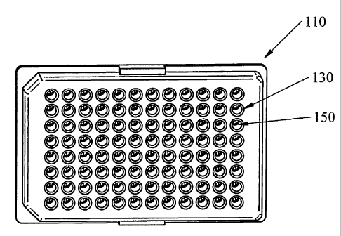
[00016] Figurel.
Illustration of an embodiment of the multi-well assay plate having 96 wells
and a pair
of functionally equivalent conductors in the form of impedance-measuring
electrodes
within each well.
[00017] Figure 2.
Illustration of an upper-plate with through holes before being sealingly
affixed to a
bottom-plate.
[00018] Figure 3.
Illustration of a top view of an impedance measuring electrode area from a
bottom
plate according to a preferred embodiment of the device
[00019] Figure 4.
Illustration of various conductor configurations
[00020] Figure 5
Illustraton of an expanded view of a side cross-section of one embodiment of
one
microwell
[00021] Figure 6
Illustration of one embodiment of the electrode-electric contact pad
connection
configuration
[00022] Figure 7.
Illustration of the direct electrical connection made between the bottom
surface of the
impedance measuring electrodes and the contact pin of an associated
measurement
system found in an alternative embodiment of the device
6
CA 02588447 2007-05-23
WO 2006/104839 PCT/US2006/010574
[00023] Figure 8.
Illustrates the current signal received by a detector and the associated
impedance
generated by wells from a preferred embodiment of the multi-well assay plate
of the
present device.
[00024] Figure 9.
96 kinetic impedance plots from the 96 wells of a specific embodiment of the
inventive device (particularly, the plate of Example 1.) are generated
simultaneously
during a cell activation experiment.
[00025] Figure 10.
Graph of maximum impedance for each well of Figure 9 from a specific
embodiment
of the inventive device (particularly, the plate of Example 1.) as a function
of
antagonist concentration to determine the IC50 of each antagonist. The graph
displays
the plate architecture's ability to determine the relative potencies of the
different
antagonists
[00026] Figure 11.
96 kinetic graphs of impedance measurements from the 96 wells of a specific
embodiment of the inventive device (particularly, the plate of Example 2
[00027] Figure 12.
Histogram comparing the magnitude of the impedance responses from each of the
compounds in the wells of a specific embodiment of the inventive device
(particularly, the plate of Example 2.).
[00028] Figure 13.
96 kinetic graphs of impedance measurements from the 96 wells of a specific
embodiment of the inventive device (particularly, the plate of Example 3).
7
CA 02588447 2007-05-23
WO 2006/104839 PCT/US2006/010574
DETAILED DESCRIPTION OF THE DEVICE
[00029] The device includes instrumentation and methods for conducting a
variety of different types of measurements. The device includes assay plates,
plate
components, and methods for performing impedance-based cellular assays. The
present device describes several novel configurations and/or materials for
functionally
equivalent conductors in assay plates, particularly in multi-well assay
plates.
[000301 As shown in Figure 1, the device relates to a single well or multi-
well
plate 110 for conducting one or more assays, the plate being formed from an
upper
plate and a bottom plate, and the assay plate having a plurality of wells 130
(and/or
chambers) and a pair of functionally equivalent conductors 150 within each
well or
chamber. According to one embodiment of the device 210 (displayed in Figure
2),
the upper plate 220 is a unitary molded structure made from rigid
thermoplastic
material such as polystyrene, polyethylene, polypropylene, polycarbonate, or
any
other plastic that can be injection molded, machined, or otherwise fabricated
into the
desired configuration. The bottom-plate 260 is made from polyethylene
terephthalate
(also commonly known as mylar or PET), polyimide, polycarbonate, polystyrene,
or
cyclo-olefin polymer (COP). In an alternative embodiment, the upper-plate 220
and
bottom-plate 260 material may comprise a combination of plastics and may
comprise
a plastic mixed with high impact polystyrene to reduce the brittleness of the
material.
Alternatively the upper 220 and bottom plates 260 may be formed from any
material
that can be molded into an appropriate shape. Materials such as plastics,
elastomers,
ceramics, composites, glass, carbon materials, or the like can be used. The
upper-
plate 220 and bottom-plate 260 are preferably formed from a material that is
generally
impervious to reagents typically encountered in biological assays, resistant
to the
adsorption of biomolecules, impervious to water and to organic solvents that
are
typically used to dissolve chemical libraries, and can withstand modest levels
of heat.
8
CA 02588447 2007-05-23
WO 2006/104839 PCT/US2006/010574
The upper-plate 220 and bottom-plate 260 are additionally made from a material
that
is sufficiently inexpensive to allow the devices to be disposed after one use,
without
large economic or ecological impacts.
[00031] The bottom plate 260 can be etched in a plasma-containing chamber in
order to clean the surface of contaminants and in order to modify the normally
hydrophobic substrate material. This treatment is known to enhance the
attachment
and viability of certain cell types and is used commonly in disposable
laboratory
plastics where cell growth is desired.
[00032] Flatness of the upper plate 220 is required so that the plate 210,
when
introduced into the assay system, can be effectively temperature controlled.
The
microplate 210 is pressed against the temperature control surface throughout
the assay
in order to maintain constant the temperature of the well contents. The
temperature
control surface may be a flat block of aluminum with holes through which the
electronic connection pins of an associated impedance measurement system
protrude.
Altematively, in order to enhance the contact between the microplate 210 and
the
temperature control surface, a compliant thermally conductive layer may be
included
between the temperature control surface and the device
[00033] Temperature control of the assays, typically between room temperature
and 37 degrees Celsius (or 42 degrees Celsius for insect cells), is important
for two
reasons. Firstly, the cell activation assays performed in the devices are
quantified
using impedance difference before and after chemical compounds are introduced
to
the cells. Non-specific changes in the impedance due to changes in the
temperature
of the buffer or cells during the assay would negatively impact the precision
measurements that are desired. Secondly, it is known that biological activity
of all
types, from simple molecular interactions to complex cellular signaling
pathways, can
be sensitive to changes in temperature. For these responses, temperature
control of
the devices during the assays are important, and controlling to within 1
degree of a
set-point, or alternatively 0.5 degrees, or further to within 0.1 degrees, is
desired.
[00034] Although the plates may be of any thickness, the bottom-plate 260
thickness is preferably optimized to allow maximum transparency and maximum
9
CA 02588447 2007-05-23
WO 2006/104839 PCT/US2006/010574
thermal conductivity (since the temperature of the well contents is controlled
by
placing the plate bottom in contact with a temperature controlled surface).
The
thickness of the upper plate and bottom plate is in the range of 0.001 inches
to 0.043
inches, with an additionally preferable thickness being on the order of 0.005
inches.
The bottom-plate 260 thickness and material selection preferably yield
transparency
that is sufficient to allow visual inspection of the cells growing at the
bottom of the
wells 230. The bottom-plate 260 is preferably thin enough to resemble a
plastic film
that is then adhered to the bottom of the upper plate 220.
[00035] Sealingly-affixing the upper-plate 220 and the bottom-plate 260
together composes the assay plate 210. The resulting microplate prevents
leakage of
fluid from any of the wells, preventing both leakage from the plate and
leakage
between wells. The sealing method must also result in a construction that is
stable to
exposure to media, buffer and solvents typically used in the applications
experiments.
Plates can be expected to remain in contact with these fluids for several
days, and it is
required that the bonding method remain unchanged during this period.
Conversely,
the contents of the wells must in no way be changed by the sealing method. For
example, adhesives used in the bonding process must be chosen carefully to
avoid
adverse effects on cell growth or cell responses during the assays.
[00036] According to one embodiment, an adhesive layer 240 is employed to
both attach the upper-plate 220 to the bottom-plate 260 and also to provide
sealing
between the wells. The adhesive layer 240 preferably comprises die cut
adhesive
transfer tape (consisting of adhesive alone or adhesive-faced film) and/or
curable
adhesives (e.g., air curing cyanoacrylics or UV-curing materials) applied as a
thin
layer across the entire bonding surface and/or around each well. The chemical
properties of the adhesive should be chosen so that there is no adverse effect
on cell
growth or the response of cells during the assay. The flexibility of the
bottom plate
260 allows easy bonding of the bottom plate 260 to the upper plate 220 with
adhesive.
[00037] In an alternative embodiments, the upper 220 and bottom 260 plates
are sealingly-affixed using insert molding (or thermal bonding) or ultrasonic
bonding.
In the case of insert molding, the bottom plate 260 is placed inside an
injection-
molding machine and the top plate 220 is molded directly onto the bottom plate
260.
CA 02588447 2007-05-23
WO 2006/104839 PCT/US2006/010574
The molten plastic bonds to the bottom plate 260 and then cools. In the case
of
ultrasonic bonding, the top 220 and bottom 260 plates are pressed together
while high
frequency vibrations create local melting and bonding between the plastics of
the top
220 and bottom plates 260.
[00038] Through holes 215 formed in the upper-plate 220 form the wells 230 of
the assay plate 210 when the upper-plate 220 is sealingly affixed to the
bottom-plate
260. The through-holes 215 are preferably injection molded or machined in the
upper-plate 220, and are typically cylindrical, rectangular, or conical in
shape with
diameters of approximately lmm to 28mm. The diameter of the through holes 215
for a 96 well plate is more preferably lmm to 7mm. Typically for injection
molding,
there is a slight draft of the holes 210 with the diameter at the top being
slightly larger
than the diameter at the bottom. The diameter is optimally chosen to conserve
the
amount of materials required to complete an assay and to minimize the well
bottom
surface area, thus minimizing the number of cells required in order to perform
the
assay. According to one preferred embodiment of the device, an assay plate 210
comprises one or more assay wells 230 or chambers (e.g., discrete locations on
an
assay plate surface where an assay reaction occurs and/or where an assay
signal is
emitted). Additional embodiments contain two or more, six or more, 24 or more,
96
or more, 384 or more, 1536 or more, or 9600 or more wells. According to one
particular embodiment, the assay plate is a multi-well assay plate having a
standard
well configuration of 6 wells, 24 wells, 96 wells, 384 wells, or 1536 wells.
[00039] According to the device, a plurality of functionally equivalent
conductors 250 in the form of impedance measuring electrodes is incorporated
into
each of the wells. The present device describes several novel configurations
and
materials for electrodes in multi-well sample plates. The impedance measuring
electrodes 250 are formed in an array on the top surface of the bottom-plate
260 such
that after the upper-plate 220 containing the through-holes 215 which comprise
the
well walls is sealingly-affixed to the bottom plate 260, the functionally
equivalent
electrodes 250 reside in the bottom of the formed wells 230. The plurality of
impedance measuring electrodes 350, illustrated in Figure 3, complete a
circuit 310 in
the bottom 380 of each micro-assay plate well 330 which allows the impedance
changes during cell activation to be monitored. In contrast to the
electrochemical
11
CA 02588447 2007-05-23
WO 2006/104839 PCT/US2006/010574
sensors used in redox reactions in which oxidation occurs at the anode and
reduction
occurs at the cathode, the impedance-measuring electrodes of this device are
not
consumed and no oxidation or reduction occurs at the electrode surfaces. The
electrodes are chemically inert. For the impedance measurements associated
with this
device, each of the conductors 350 is functionally equivalent, with cells on
each of the
electrodes contributing to the impedance changes that occur upon cellular
activation.
1000401 The impedance-measuring electrodes 350 are formed of a single or
multiple layer of a conductive material. The conductive material is preferably
a metal
or a non-metallic conductive material with a surface that is amenable to cell
growth.
Preferable metallic conductive materials include gold, silver, and platinum.
Preferable non-metallic conductive materials include ITO, conducting polymers,
and
carbon fibers. Preferable conductive materials are inert to the organic and
inorganic
compounds typically used in biological assays and will not be subject to
electrochemical reactions at the low voltages used in impedance measurements
(100mV).
[000411 The impedance-measuring electrodes 350 may be fabricated by a
negative process of removing metal from a uniform layer across the substrate
material. The uniform metal may be sputtered or evaporated using traditional
sputtering or evaporating means on the surface of the bottom-plate, creating a
thin
film that is nanometers to microns in thickness. A preferred thickness is 50
nm. A
50nm layer of gold is semi-transparent and allows the inspection of cells on
the
electrodes using common laboratory microscopes. Alternatively, the metal layer
may
be electroplated or laminated onto the surface of the bottom plate. After
being
applied, the uniform metal layer may be patterned to form the impedance-
measuring
electrodes using photolithographic exposure and chemical etching or
alternatively,
the metal may be removed by a laser ablation process. Metal that is not
removed
comprises the resulting electrodes.
[00042] Alternatively, the impedance-measuring electrodes 350 may be
fabricated by the additive process of a printing process such as screen-
printing or pad
printing of a conductive ink. Conductive inks containing silver, gold,
platinum,
and/or carbon particles may be used for this purpose. Conductive inks from
12
CA 02588447 2007-05-23
WO 2006/104839 PCT/US2006/010574
companies such as Dupont and Acheson are typical of those used. Gold is a
preferable
conductive material in that the particles are highly conductive and the gold
is highly
inert, making the surface of the electrodes resistant to degradation by the
atmosphere
and by fluids that may be used in the assay wells 330. Also, due to its inert
nature,
gold is not toxic to cells. Gold particles in the range of 0.25 to 10 microns
may be
used in inks that are applied to a thin layer to form the electrodes.
Additionally, the
electrodes may be formed from the combination of metal layers and conductive
ink.
[00043] The dimensions of the electrode's 350 features are in the range of 5
microns to 3 millimeters, with 10 microns to 250 microns being a preferable
range.
Similarly, the spacing between the electrodes 350 may be from 5 microns to 3
millimeters, with a preferred range being 10 microns to 250 microns. Smaller
spacing
of the features is preferable as the electrical circuits formed by such spaced
features
are less sensitive to thermal and evaporative changes to the buffer used in
the assays.
Electrode geometries allowing the creation of an area of uniform electric
field over
the detection surface area at the bottom of the microplate are preferable. In
one
embodiment, the electrode geometry is an interdigitated finger structure with
finger
and gap widths that are comparable in dimension. Alternate geometries include
simple designs with two opposing electrodes in the shape of lines or circles,
as
displayed in Figs. 4.
[00044] In order to provide for connections between the electrodes inside the
wells and an impedance measuring system with which the plate will work in
conjunction, the devices are provided with an array of electrically conductive
electrical contact pads (or electrical contact pads) situated on the bottom
surface of
the bottom plate and an array of electrically conductive vias connecting these
contact
pads to the electrodes on the top surface of the bottom plate. As shown in
Figure 5
(an expanded view of a well side cross section), electrical contact with the
impedance
measuring system is made through electrical contact pins 565, that contact the
device
when the device is placed in an associated impedance measurement system.
Electrical contact pads 525, situated on the bottom surface of the bottom
plate 560,
are round or oval targets of conductive material, such as sputtered gold or
silver ink.
The size of the pads is such that tolerances in the locations of the pins 565
and in the
placement of the plate into the system will always ensure contact. The pads
may be
13
CA 02588447 2007-05-23
WO 2006/104839 PCT/US2006/010574
patterned onto the bottom plate 560 using the same processing steps used to
pattern
the electrodes 550 on the top surface of the bottom plate 560, i.e. sputtering
and
removal of gold, or screen printing of conductive ink, such as silver ink.
[00045] In order to make electrical contact between the electrical contact pad
525 and the electrodes 550, which are on opposite surfaces of the bottom plate
560,
electrically conductive vias 545 are fabricated into the bottom plate 560. The
vias
545 are created by first drilling an array of holes in the bottom plate 560.
Drilling
may be performed by conventional machining, by laser machining, or by
ultrasonic
drilling. Laser and ultrasonic drilling may be used in order to drill a bottom
plate
prepared from fragile material such as glass. For bottom plates 560 prepared
from
thin plastic films, laser drilling is a fast and convenient way of drilling
holes on the
order of 150 microns in diameter. After fabrication of the holes, the holes
can be
made into conductive vias 545 by coating or filling them with conductive
material
that contacts the electrodes 550 and electrical contact pads 525 on the
opposite
surfaces of the bottom plate 560. Additionally, the electrically conductive
electrical
contact pads and conductive vias may be formed from a combination of metal
layers
and conductive ink.
[00046] In one embodiment, in which sputtered gold is used to create both the
electrodes 550 and pads 525, the holes are drilled before the sputtering
process. In
this way, sputtered gold can also coat the inner surfaces of the drilled
holes, forming
the conductive via. In another embodiment, in which the electrodes 550 and
pads
325 are screen printed using conductive inks, the previously-drilled holes can
be
coated with the ink during the printing of these other features.
[00047] In the alternative embodiment illustrated in Figure 6, the electrodes
650 are prepared from sputtered 50 nm gold, and the pads 625 are printed with
conductive silver ink. An additional electrical pad 625 is added to the top
surface of
the bottom plate 660 in order to ensure that electrical continuity between the
via 645
and the electrode 650 is made. In this embodiment, a top electrical conductive
ink
pad 625 is screen printed on the top surface of the bottom plate 660,
intersecting both
the drilled hole and the electrode 650. During this printing step, conductive
ink also
fills into the via hole 645. Ink printed to form the electrical contact pad
625 printed
14
CA 02588447 2007-05-23
WO 2006/104839 PCT/US2006/010574
on the bottom surface of the bottom plate 660 thus makes contact with ink
printed to
form the top electrical pad 625.
[00048] In an additional embodiment, electrical connection is made directly
between the measurement system pins 765 and the bottom surface of the
electrodes
750 as illustrated in Figure 7. Drilled holes 755 in the bottom plate 760
allow access
to the electrodes 750 by the measurement system pins 765. In this case, the
electrode
material must be robust enough to extend across the top of the hole 755
opening and
to remain intact during the various stages of device fabrication. The holes
755 must
be sized small enough in order to allow the electrode material to robustly
cover the
top of hole 755. Conversely, the holes 755 must be sized large enough as to
allow
alignment to and contact with the entire array of measurement system pins 765
accounting for the tolerances in the plate location in the instrument and the
pin 765
locations in the instrument. For electrodes fabricated from 10 microns of
conductive metal, hole diameters of 0.010" to 0.080" are suggested. Other,
thicker or
more robust electrodes materials, may allow larger holes to be covered.
Conversely,
thinner or less robust materials would only be used to cover smaller holes.
[00049] Making contact with the bottom surface of the microplate instead of
connecting through the top of the wells or along the edge of the microplate
offers
distinct advantages. This configuration allows the area around the top of the
plate to
be free for access for injection of chemical compounds into the wells while
measurements are being taken. Injection may be performed using a large
pipetting
head with an array of 96 or more pipetting tips. In addition, the large
surface area
available underneath the device allows for a much larger number of electrical
connections to be made. This is important for two reasons. Firstly, it allows
for the
connection of increasing numbers of electrodes that would be incorporated into
higher
density microplates with 384, 864, 1536 or more wells. Secondly, connection of
each
individual electrode to a touchpad in this manner allows a homogeneous plate
architecture where each well is electrically identical to every other well in
the plate.
This architecture allows the simultaneous measurement of an arbitrary number
of
wells simultaneously, limited only by the complexity of the impedance
measurement
electronics. Other devices described in the art, in order to reduce the number
of
electrical contacts, provide for common electrical contact with multiple
electrodes; for
CA 02588447 2007-05-23
WO 2006/104839 PCT/US2006/010574
example, an electrical bus may connect to all of the wells in each row of the
device.
With this strategy, however, there are two disadvantages. First, only one well
per row
can be measured at once without potential coupling or interferences between
wells.
Second, a problem with an electrical contact to a row would disable the entire
row.
[00050] The bottom contact arrangement also ensures that, even for a device
with a large number of connections, traces never need to cross in the
microtiter plate.
Thus, a single conductive layer can be fabricated on the bottom plate, keeping
it
simple and inexpensive to fabricate With this strategy, complex and expensive
multi-
layer electrical devices are required only in the to the impedance measuring
instrument itself.
[00051] Insulating layers on top of the electrodes can be included in order to
further define the exposed electrode geometry, to eliminate the electrical
contribution
of certain areas of the electrodes, and to facilitate the electrical
connection to an
associated impedance measurement system. In one example, it may be desired to
concentrate the measurement solely in the center of the microtiter plate wells
to
reduce the amount of conductive material required to perform the assay and to
reduce
the overall manufacturing costs. For example, the use of gold in the well
center is
preferred, but the costs of gold makes its use as the entire conductive
element
prohibitive. Although the use of cheaper conductive materials, such as silver,
may be
desirable, the toxicity of silver may prohibit its use in the well center
area. To
facilitate the concentration of the measurement to the well center, a
dielectric ink may
be printed to mask the electrode areas outside of the well centers. In such an
example,
the electrodes may be fabricated from two conductive materials where the first
material forms the part of the electrode that lies in the center of the well
and that will
be in contact with the assay contents while a second material forms a portion
of the
electrical path between the first material and the conductive via. ,
[00052] As an alternative to the device fabricated from an upper plate and a
bottom plate, the device may be fabricated in one piece. A microtiter plate
may be
injection molded directly on to a conductive lead frame placed in the
injection
molding machine. The result from the insert molding process is an array of
impedance measuring electrodes that are sealingly encapsulated by the injected
plastic
with exposed top surfaces of the electrodes residing at the bottom of the
formed wells
16
CA 02588447 2007-05-23
WO 2006/104839 PCT/US2006/010574
and the bottom surfaces of the electrodes exposed at the locations of
electrical contact
on the bottom of the microtiter plate. . Portions of the lead frame that
mechanically
connect the array of electrodes together during the manufacturing process but
are
unnecessary from an electrical standpoint can be broken apart in a post
processing
step.
[00053] As displayed in Figure 8, the electric field 825 generated by the
electrodes 830 extends from the electrode surface 835 at the bottom of the
well 880 to
a depth equal roughly to the gap between the electrodes 830. Cells 845 that
are
growing on the bottom of the well 880 and on the electrodes 830 experience
this
electric field 825. Measurement of the total current in the circuit, comprised
of the
intracellular (Itc) and extracellular (lec) currents, allows calculation of
the cell layer
impedance by the impedance measurement system. In addition, non-adherent cells
that have sedimented to the bottom of the wells and are within the electric
field can
additionally be assayed using this technology.
[00054] For the impedance measurement, which is performed with alternating
voltage, a detector measures the current resulting from the applied
alternating voltage.
Both the magnitude of the resulting current and the phase (relative to the
applied
voltage) are part of the impedance, which is a complex number made up of real
and
imaginary components. The associated measurement system may measure both
components or either. Typically, a 100 mV (rms) signal is applied and currents
on the
order of 0.1 to 1 mA (rms) are measured. The system (microtiter plate and
associated
impedance measurement system) should be designed to work with voltages as high
as
300 - 400 mV. Essentially, the lower limit on the applied voltage is set by
the
amount of noise that can be tolerated. Voltages as low as 10-20 mV are more
likely
to be typical.
[00055] Typically, when identification of a particular microtiter assay plate
is
required in an assay system, bar code labels are applied to top or edges of
the
microplate. In the current device, it was desired to incorporate into the
fabrication of
the microplate itself a feature that would allow identification of the plate
type to the
assay system. This would obviate the need for a separate bar coding label and
a
17
CA 02588447 2007-05-23
WO 2006/104839 PCT/US2006/010574
separate bar code reader inside the instrument. In one embodiment, the plate
identification can be accomplished by a number of mechanisms. Optically
readable
features, fabricated into the plate bottom at the same time as the electrical
contact
pads, could be read with a stationary reflective optical sensor as the plate
moves into
the assay system instrument. Electrically readable features, fabricated into
the plate
bottom at the same time as the electrical contact pads, could be read using
the same
electrical contact pins and electronics of the impedance measuring-system.
Mechanical features on the upper plate such as holes, indentations, or steps
could be
read using optical or mechanical switches. RFID tags could be incorporated
into the
plate bottom or top which would be readable by a nearby unit inside the
associated
impedance measurement system. Another option for enabling plate ID allowing a
larger amount of information to be stored and read is the incorporation of a
microchip
such as a PROM (Programmable read-only memory chip) or EEPROM (electronically
erase-able programmable read-only memory chip). Each mechanism could
additionally incorporate an error detecting code which would detect system
errors
before reading the plate.
[00056] The multi-well assay plates of the present device may be used with
adherent and non-adherent cellular species, molecular species, viral
particles, and
bacteria, and may be used once or may be used multiple times. The assay plates
are
well suited to applications where the plates are disposable depending on the
biological
nature of the well inhabitants.
APPLICATIONS
[000431 The Impedance Measurement Instrument
[000441 The devices described in the examples below interface with a custom
impedance measurement system in three ways. 1) The electrical contact pads on
the
bottom of the assembled device contact electrical contact pins on the
instrument.
Electrical connection of each well leads to an impedance measurement
electronics.
2) The bottom surface of the device rests against a thermally controlled
surface,
allowing the temperature of the contents of the devices' wells to be
controlled. 3)
The wells of the top plate align with an automated pipetting device of the
instrument,
18
CA 02588447 2007-05-23
WO 2006/104839 PCT/US2006/010574
allowing the addition of different chemical compounds to be added to each of
the
wells during the impedance measurements.
[00045] Impedance measurements are comprised of impedance magnitude and
impedance phase. Both of these quantities can be used to calculate the real
part of
the complex impedance. Comparirig the impedance changes of different wells
after
the addition of the chemical compounds allows the determination of whether and
to
what degree the chemical compounds affect the cells.
Example 1.
A bottom plate was fabricated from a lmm thick 122mm x 79 mm BorofloatTM glass
substrate. Holes in the glass (0.030") were drilled using an ultrasonic
process. 1.6
microns of gold was sputtered onto both the top and bottom surfaces of the
glass. At
the same time, sputtered gold coated the inside surface of the drilled holes,
forming an
electrical via between to top and bottom surfaces of the glass.
Photolithographic
exposure and chemical etching techniques were then used to pattern the
impedance
measuring electrodes on the top surface of the bottom plate and to form the
electrical
contact pads on the bottom surface of the bottom plate. The electrodes were a
pair of
interdigitated finger combs with finger sizes of 30 microns in width and 2.5
mm in
length. Gaps between the fingers on opposing combs were 30 microns.
The bottom plate was bonded using UV curable epoxy to a machined polystyrene
upper plate containing 96 through holes in an 8 x 12 array.. The 96 holes,
each 6
mm in diameter and 12 mm deep, were aligned on top of the electrode features
on the
bonded bottom plate in order to form 96 wells.
Into each well of the 96-well device, 40,000 CHO cells transfected with the ml-
muscarinic receptor were pipetted added along with 150uL growth media. The
device
was placed in an incubator at 37C and 5% COZ environment for 18 hours in order
to
allow the cells to settle to the bottom of the wells and to attach and grow
across the
surface of the well bottom and electrode. Prior to performing the cell
response
experiment, the growth media was removed and was replaced with 136mM Hanks
Hepes buffer with 0.1% BSA. Six antagonist titrations, with decreasing
concentration
19
CA 02588447 2007-05-23
WO 2006/104839 PCT/US2006/010574
from left to right, were added from Row A to Row F (inclusive) and allowed to
incubate for 15 minutes. To Rows G and H were added the negative control
(matching buffer). The device was placed into the impedance measurement system
and allowed to thermally equilibrate to the system at 28C. After the 15-minute
incubation, a single concentration of agonist (carbachol) was added to Rows A-
G,
while a negative control (matching buffer) was added to Row H. Impedances of
each
device were measured for 5 minutes prior to and 10 minutes after agonist
addition at
20-second intervals.
In Figure 9, the impedance measurements of the 96 wells are shown as a
function of
time. It can be seen how decreased antagonist concentration gives larger cell
impedance changes. In Figure 10, responses were graphed as a function of
antagonist
concentration to determine the IC50 of each antagonist, showing the relative
potencies
of the different antagonists.
Example 2.
A bottom plate was fabricated from a 1mm thick 122mm x 79 mm polystyrene sheet
substrate. Holes in the polystyrene (0.030") were drilled. 0.5 microns of gold
was
sputtered onto the top surface of the polystyrene through a thin metal mask or
stencil
in order to create the electrode pattern. The electrodes were a pair of
interdigitated
finger combs with finger sizes of 200 microns in width and 1.5 mm in length.
Gaps
between the fingers on opposing combs were 200 microns. At the same time as
the
electrodes were created, sputtered gold coated the inside surface of the
drilled holes.
Subsequently, 0.5 microns of gold was sputtered onto the bottom surface of the
polystyrene through a thin metal mask or stencil in order to create the
electrical
contact pad pattern. At the same time, sputtered gold again coated the inside
surface
of the drilled holes, forming an electrical via between to top and bottom
surfaces of
the polystyrene. After fabrication of the gold features on the polystyrene,
the bottom
plate was plasma etched in order to increase the adherence of cells onto the
surface.
The bottom plate was bonded using W curable epoxy to a machined polystyrene
upper plate containing 96 through holes in an 8 x 12 array.. The 96 holes,
each 6
CA 02588447 2007-05-23
WO 2006/104839 PCT/US2006/010574
mm in diameter and 12 mm deep, were aligned on top of the electrode features
on the
bonded bottom plate in order to form 96 wells.
50,000 HeLa cells per well were pipetted into the wells of the device in 150
microliters MEM growth media. The cells in the device were incubated overnight
in
an incubator at 37C and 5% C02. The following day, the media was removed and
the cells gently washed 3 times with 136mM Hanks Hepes buffer. The final fluid
exchange introduced 135 microliters of 136 mM Hanks Hepes buffer with 0.1%
BSA.
The device was introduced into impedance measurement instrument, where it was
warmed to 28C. 30 minutes after the media to buffer exchange, impedance
measurements were begun. After 5 minutes of pre-drug addition impedance
measurement, a panel of chemical compounds was added to the cells in the
device.
The source of the panel was a 96 well plate containing 92 different chemical
compounds. The remaining 4 wells contained buffer only.
In Figure 11, the impedance measurements of the 96 wells are shown. It can be
easily be seen that responses of the cells to the different chemical compounds
can be
characterized both by the magnitude of the impedance changes as well as the
kinetics
and direction of the impedance responses.
In Figure 12, the magnitude of the responses from each of the compounds is
compared in a histogram format.
Example 3.
Bottom plates were fabricated from a 0.005" thick polyester sheet substrate.
Holes in
the polystyrene (0.15 mm) were laser drilled in a pattern to match with the
electrical
vias to be created in a later step in the bottom plate. Conductive silver ink
was used
in a screen printing process to create the electrical contact pads on the
bottom surface
of the bottom plate material and to fill into the drilled via holes.
Subsequently, a
second printing pass with silver ink was used to print features on the top
surface of the
bottom plate, leading from the drilled vias towards a location near where the
center of
the microplate wells will be created when the bottom plate and upper plate are
bonded. Subsequently, fingers of gold ink were printed creating an
interdigitated
21
CA 02588447 2007-05-23
WO 2006/104839 PCT/US2006/010574
finger pattern between the two silver leads. Each gold finger overlapped on
one end
with one of the silver leads. In the last printing step, a dielectric ink was
printed, '
covering the entire surface top surface of the bottom plate except a rectangle
that left
lengths of the gold fingers exposed. By covering the tips of the gold fingers
with
insulating dielectric, the total length of exposed gold finger was determined
by the
dimension of the dielectric window and the finger widths. The printed bottom
plate
material was plasma etched for 4 minutes in an oxygen atmosphere in order to
increase cell adhesion. Following etching, individual bottom plates were cut
from
the sheet.
Each bottom plate was bonded using 0.002" adhesive transfer tape to an
injection
molded polystyrene upper plate containing 96 through holes in an 8 x 12 array.
The
96 holes, each 6.55 mm in diameter, were aligned on top of the electrode
features on
the bonded bottom plate in order to form 96 wells.
Into each well of the 96-well device, 50,000 HeLa cells were pipetted added
along
with 150uL growth media. The device was placed in an incubator at 37C and 5%
C02 environment for 18 hours in order to allow the cells to settle to the
bottom of the
wells and to attach and grow across the surface of the well bottom and
electrode.
Prior to performing the cell response experiment, the growth media was removed
and
was replaced with 136mM Hanks Hepes buffer with 0.1 % BSA. The device was
placed into the impedance measurement system and allowed to thermally
equilibrate
to the system at 28C. A panel of 141igands with 6 replicates each was added to
seven
rows (B through H) of the device with 2 ligands per row. To Row A was added
the
negative control (buffer). Impedances of each device were measured at 20
second
intervals for 5 minutes prior to and 10 minutes after ligand addition. In
Figure 13, the
impedance changes with time for each well are plotted. Similar response
kinetics and
characteristics can be grouped together (e.g., D01-D06, D06-12, and E01-06
appear
similar) indicating that cellular responses to these ligands are related. Two
electrically open wells did not provide meaningful data as noted by the
impedance
measurement system (wells DO1 and A07).
22
CA 02588447 2007-05-23
WO 2006/104839 PCT/US2006/010574
SUMMARY
While the above is a complete description of possible embodiments of the
device,
various alternatives, modifications, and equivalents may be used. For instance
a
person skilled in the art will appreciate that the impedance measuring
electrode
geometry is not limited to an interdigitated fmger design. Other conductor
geometries
may alternatively be used. Further, all publications and patent documents
recited in
this application are incorporated by reference in their entirety for all
purposes to the
same extent as if each individual publication and patent document was so
individually
denoted. The above description should be view as only exemplary embodiments of
the device, the boundaries of which are appropriately defined by the metes and
bounds of the following claims.
23