Note: Descriptions are shown in the official language in which they were submitted.
CA 02589028 2007-05-31
WO 2006/060302 PCT/US2005/042871
LATERAL TRENCH FIELD-EFFECT TRANSISTORS IN WIDE
BANDGAP SEMICONDUCTOR MATERIALS, METHODS OF MAKING,
AND INTEGRATED CIRCUITS INCORPORATING THE TRANSISTORS
This application is related to U.S. Patent Application No. 60/585,881, filed
July 8, 2004, and U.S. Patent Application No. 11/000,222 filed December 1,
2004,
entitled: "Normally-Off Integrated JFET Power Switches in Wide Bandgap
Semiconductors and Methods of Making". Each of the aforementioned
applications is incorporated by reference herein in its entirety.
BACKGROUND
Technical Field
The present invention relates generally to lateral field effect transistors
(FETS) with vertical channels, and in particular, to such transistors formed
in wide
bandgap semiconductor materials. This inverition also relates to monolithic
integrated circuits comprising these transistors.
Background of the Technology
Wide bandgap semiconductor materials (with EG > 2eV) such as silicon
carbide (SiC) or Group III nitride compound semiconductors (e.g., gallium
nitride
GaN) are very attractive for use in high-power, high-temperature, and/or
radiation
resistant electronics. SiC power rectifiers and RF transistors are now
-1-
CA 02589028 2007-05-31
WO 2006/060302 PCT/US2005/042871
commercially available, and SiC power switches as well as GaN microwave
transistors are expected to appear in the commercial market in the near
future.
Because of the fundamental differences in material properties and
processing technologies, traditional Si or GaAs integrated circuit (IC)
technologies
such as Complementary Metal-Oxide-Semiconductor (CMOS) or Direct Coupled
FET Logic (DCFL) cannot in most cases be easily transferred to wide bandgap
semiconductor industry. Several attempts at fabricating SiC NMOS and CMOS
digital and analog ICs have been reported in the last decade (e.g., [1], [2]).
A
monolithic CMOS integrated device in SiC and method of fabricating the same
have been patented in 2002 [3]. Moreover, recent development of SiC Lateral
DMOS Field-Effect Transistors (LDMOSFETs) (e.g., [4], [5]) theoretically
allows
for the monolithic integration of MOSFET-based control circuitry and power
switch for use in Smart Power electronics. However, certain issues limit the
use of
MOSFET-based SiC integrated circuits in the applications where high
temperature
and/or radiation tolerance is required. The first such issue is on-state
insulator
reliability due to much smaller conduction band offset of SiC to Si02 as
compared
to that of silicon [6], [7]. This issue becomes even more significant at high
temperature and extreme radiation environment. Other issues include: low
inversion channel mobility due to high interface state density at the SiC/SiO2
interface and high fixed charge density in the insulator; and significant
threshold
voltage shift with temperature due to ionization of interface states.
2
CA 02589028 2007-05-31
WO 2006/060302 PCT/US2005/042871
Another transistor candidate for the use in SiC ICs is a Metal
Semiconductor Field-Effect Transistor (MESFET). Although SiC MESFET
monolithic microwave integrated circuits (MMICS) have received significant
attention in the last decade (e.g., [8]), there have been few published
attempts to
build SiC MESFET logic and analog circuits (e.g., [9]).
An alternative to the MOSFET and MESFET approaches is the use of
lateral JFET-based ICs. An example of a vertical channel JFET employing a
recessed gate structure can be found in U.S. Patent No. 4,587,712 [10]. An
example of a lateral JFET formed in SiC can be found in U.S. Patent No.
5,264,713 [11]. Enhanced-mode JFET digital ICs with resistive load have also
been reported [12]. JFET based ICs can also be implemented in either
complementary (n-type and p-type channels as disclosed in U.S. Patent No.
6,503,782 [13] or enhanced-depletion (n-type channels) forms. SiC JFETs have
proven to be radiation tolerant while demonstrating very insignificant
threshold
voltage shift with temperature [14]. A major deficiency of this approach has
been
difficulties achieving monolithic integration of low voltage control circuitry
with
power switches for Smart Power electronics.
3
CA 02589028 2007-05-31
WO 2006/060302 PCT/US2005/042871
SUMMARY
According to a first embodiment, a junction field-effect transistor is
provided which comprises:
a substrate having opposed first and second major surfaces;
a drain layer of an n-type semiconductor material on the first major surface
of the substrate;
a drift layer of an n-type semiconductor material on and non-coextensive
with the drain layer such that portions of the drain layer are exposed, the
drift layer
having a lower conductivity than the drain layer;
one or more discrete raised regions in spaced relation on the drain layer,
each of the raised regions comprising a channel region of an n-type
semiconductor
material on the drift layer and a source region of an n-type semiconductor
material
on the channel region, the material of the source region having a higher
conductivity than that of the channel region;
a gate region of a p-type semiconductor material on the drift layer adjacent
the one or more raised regions and forming a rectifying junction with n-type
material of the drift layer and the channel region(s);
ohmic contacts on the gate and source regions and on exposed portions of
the drain layer.
According to this embodiment, the source region can be coextensive with the
channel region.
4
CA 02589028 2007-05-31
WO 2006/060302 PCT/US2005/042871
According to a second embodiment, a semiconductor device is provided
which comprises:
a substrate having opposed first and second major surfaces; and
a first and a second junction field-effect transistor each on a discrete
location on the first major surface of the substrate, each of the junction
field-effect
transistors comprising:
a drain layer of an n-type semiconductor material on and non-coextensive
with the first surface of the substrate such that portions of the substrate
surrounding the drain layer are exposed;
a drift layer of an n-type semiconductor material on and non-coextensive
with the drain layer such that portions of the drain layer are exposed, the
drift layer
having a lower conductivity than the drain layer;
one or more discrete raised regions in spaced relation on the drift layer,
each of the raised regions comprising a channel region of an n-type
semiconductor
material on the drift layer and a source region of an n-type semiconductor
material
on the channel region, the material of the source region having a higher
conductivity than that of the channel region;
a gate region of a p-type semiconductor material on the drift layer adjacent
the one or more raised regions and forming a rectifying junction with n-type
material of the drift layer and the channel region(s);
ohmic contacts on the gate and source regions and on exposed portions of
the drain layer.
CA 02589028 2007-05-31
WO 2006/060302 - PCT/US2005/042871
The first junction field-effect transistor can have a first threshold voltage
and the
second junction field-effect transistor can have a second threshold voltage
different
than the first threshold voltage.
According to a third embodiment, a field-effect transistor is provided which
comprises:
a substrate having opposed first and second major surfaces;
a drain layer of an n-type semiconductor material on the first major surface
of the substrate;
a drift layer of an n-type semiconductor material on the drain layer and
non-coextensive therewith such that portions of the drain layer are exposed,
the
drift layer having a lower conductivity than the drain layer;
one or more discrete raised regions in spaced relation on the drift layer,
each of the raised regions comprising a channel region of an n-type
semiconductor
material on the drift layer and a source region of an n-type semiconductor
material
on the channel region, the n-type semiconductor material of the source region
having a higher conductivity than that of the channel region;
a metal layer on the drift layer adjacent the one or more raised regions and
forming a metal-semiconductor rectifying junction with the drift layer and the
channel region(s); and
ohmic contacts on the source region and on exposed surfaces of the drain
layer. According to this embodiment, the source region can be coextensive with
the channel region.
6
CA 02589028 2007-05-31
WO 2006/060302 PCT/US2005/042871
The field-effect transistor according to any of the aforementioned
embodiments can comprise a plurality of raised regions. The raised regions can
be
elongate, having a major and a minor dimension. The raised regions can be
oriented such that the major dimensions of the raised regions are parallel to
one
another. The plurality of raised source regions can also be spaced apart from
one
another at regular intervals in the direction of the minor dimension. The gate
region can comprise a plurality of fingers extending between adjacent raised
regions.
According to a fourth embodiment, a field-effect transistor is provided
which comprises:
a substrate having opposed first and second major surfaces;
a drain layer of an n-type semiconductor material on the first major surface
of the substrate; and
a drift layer of an n-type semiconductor material on the drain layer and
non-coextensive therewith such that portions of the drain layer are exposed,
the
drift layer having a lower conductivity than the drain layer;
a gate region of a p-type semiconductor material formed in the drift layer;
a channel region of an n-type semiconductor material on the drift layer and
forming a rectifying junction with the gate region; and
a source region of an n-type semiconductor material on the channel region,
the semiconductor material of the source region having a higher conductivity
than
that of the channel region; and
7
CA 02589028 2007-05-31
WO 2006/060302 PCT/US2005/042871
ohmic contacts on the source region and on exposed portions of the drain
layer. According to this embodiment, the source, channel and drift regions can
be
coextensive. In addition, the gate region can comprise a plurality of fingers.
In the field-effect transistor according to any of the aforementioned
embodiments, the semiconductor material of the drain layer, drift layer, gate
region; channel region and source region can have an EG of at least 2 eV
(e.g., SiC
or a Group III nitride compound semiconductor material such as GaN).
In the field-effect transistor according to any of the aforementioned
embodiments, the substrate can be selected from the group consisting of: semi-
insulating; p-type; or n-type with a p-type buffer layer thereon wherein the p-
type
buffer layer forms the first surface of the substrate.
According to a further embodiment, an integrated circuit which comprises a
plurality of field-effect transistors as set forth in any of the
aforementioned
embodiments disposed on a common substrate is provided. The integrated circuit
can comprise a first field-effect transistor having a first threshold voltage
and a
second field-effect transistor having a second threshold voltage different
than the
first threshold voltage.
According to a further embodiment, a method of making a field-effect
transistor is provided which comprises selectively etching a multi-layered
structure. According to this embodiment, the multi-layered structure
comprises: a
substrate having opposed first and second surfaces; a drain layer of an n-type
semiconductor material on the first surface of the substrate; a drift layer of
an n-
8
CA 02589028 2007-05-31
WO 2006/060302 PCT/US2005/042871
type semiconductor material non the drain layer, the drift layer having a
lower
conductivity than the drain layer; a channel layer of an n-type semiconductor
material on the drift layer between and in contact with adjacent gate regions;
and a
source layer of an n-type semiconductor material on the channel region, the
source
layer having a higher conductivity than the channel layer. The method
according
to this embodiment comprises selectively etching through the source layer and
partially through the channel layer to form at least one raised region;
selectively
implanting ions of a p-type dopant in exposed portions of the channel layer
adjacent the at least one raised region; selectively etching through exposed
portions
of the implanted channel layer and underlying drift layer to expose underlying
drain layer; and selectively etching through exposed portions of the drain
layer to
expose underlying substrate thereby forming an etched structure.
According to a further embodiment, a method of making a field-effect
transistor is provided which comprises selectively implanting a p-type dopant
on a
multi-layered structure. According to this embodiment, the multi-layered
structure
comprises: a substrate having opposed first and second major surfaces; a drain
layer of an n-type semiconductor material on the first major surface of the
substrate; a drift layer of an n-type semiconductor material on the drain
layer, the
drift layer having a lower conductivity than the drain layer. The method
according
to this embodiment comprises selectively implanting the p-type dopant in the
drift
layer to form a gate region; depositing or growing a channel layer of an n-
type
semiconductor material on the implanted surface of the drift layer; depositing
or
9
CA 02589028 2007-05-31
WO 2006/060302 PCT/US2005/042871
growing a source layer of an n-type semiconductor material on the channel
layer,
the source layer having a higher conductivity than the channel layer;
selectively
etching through the source layer, the channel layer and the implanted drift
layer to
expose underlying drain layer thereby forming raised regions; and selectively
etching through portions of the exposed drain layer to expose underlying
substrate
thereby forming an etched structure.
According to a further embodiment, a method of making a field-effect
transistor is provided which comprises selectively etching a multi-layered
structure. According to this embodiment, the multi-layered structure
comprises: a
substrate having opposed first and second major surfaces; a drain layer of an
n-type
semiconductor material on the first major surface of the substrate; a drift
layer of
an n-type semiconductor material on the drain layer, the drift layer having a
lower
conductivity than the drain layer; a channel layer of an n-type semiconductor
material on the drift layer; and a source layer of an n-type semiconductor
material
on the channel region, the source layer having a higher conductivity than the
channel layer. The method according to this embodiment comprises selectively
etching through the source and channel layers to expose underlying drift layer
thereby forming at least one raised region; selectively etching through
exposed
portions of the drift layer to expose underlying drain layer; selectively
etching
through exposed portions of the drain layer to expose underlying substrate,
thereby
forming an etched structure; and depositing a Schottky metal in contact with
exposed portions of the drift layer.
CA 02589028 2007-05-31
WO 2006/060302 PCT/US2005/042871
A method according to any of the aforementioned embodiments may
further comprise an annealing treatment after the implantation of the p-type
dopant
in order to activate the dopant.
A method according to any of the aforementioned embodiments may
further comprise growing or depositing a layer of dielectric material on
exposed
surfaces of the etched structure; anisotropically etching the dielectric
material to
expose underlying portions of drain, gate and/or source regions parallel to
the first
surface of the substrate; and depositing metal on exposed portions of drain,
gate
and source regions.
In a method according to any of the aforementioned embodiments, the
semiconductor material can be SiC. When the semiconductor material is SiC, the
method can further comprise annealing after depositing metal on exposed
portions
of drain, gate and/or source regions such that metal at the
metal/semiconductor
material interface reacts to form metal silicide; and removing unreacted
metal. The
unreacted metal can be removed using an acid etch.
In a method according to any of the aforementioned embodiments, a
plurality of raised regions can be formed. The plurality of raised regions can
be
elongate and can have a major and a minor dimension. The raised regions can be
oriented such that the major dimensions of the raised source regions are
parallel to
one another. The plurality of raised source regions can be spaced apart from
one
another at regular intervals in the direction of the minor dimension.
11
CA 02589028 2007-05-31
WO 2006/060302 PCT/US2005/042871
In a method according to any of the aforementioned embodiments, multiple
etched structures can be formed on a single substrate wherein etching through
the
drain layer isolates each etched structure.
12
CA 02589028 2007-05-31
WO 2006/060302 PCT/US2005/042871
BRIEF DESCRIPTION OF THE DRAWINGS
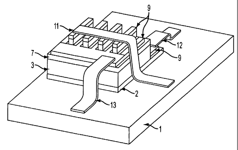
Figure 1 is a schematic three-dimensional illustration of a multi-finger
Lateral Trench JFET.
Figure 2 is a schematic diagram illustrating the fabrication process of a
single-finger Lateral Trench JFET.
Figure 3A is a schematic cross-section of a single-finger Lateral Trench
JFET fabricated on p-type substrate.
Figure 3B is a schematic cross-section of a single-finger Lateral Trench
JFET fabricated on n-type substrate with p-type buffer layer.
Figure 4A is a schematic cross-section of a single-channel Lateral
JFET with overgrown source region
Figure 4B is a schematic cross-section of a single-finger Lateral Trench
FET with Schottky gate.
Figure 5A is a schematic cross-section of a single-finger Lateral
Trench JFET fabricated on semi-insulating substrate, and schematic
presentation of
electrical connections.
Figure 5B is a schematic cross-section of a multi-finger Lateral Trench
JFET fabricated on semi-insulating substrate, and schematic presentation of
electrical connections.
Figure 6A is a schematic cross-section of two single-finger Lateral Trench
JFETs with different threshold voltages fabricated on the same die.
13
CA 02589028 2007-05-31
WO 2006/060302 PCT/US2005/042871
Figure 6B is a schematic cross-section of two single-finger Lateral Trench
JFETs with different threshold voltages fabricated on the same die including
electrical connections used to form a monolithic inverter circuit.
Figure 7A displays the measured I-V characteristics of a discrete vertical
channel power VJFET implemented for enhanced mode operation wherein the
values of the drain current shown are normalized to I m of the gate
periphery.
Figure 7B displays the measured I-V characteristics of a discrete vertical
channel power VJFET implemented for depletion mode operation wherein the
values of the drain current shown are normalized to 1 m of the gate
periphery.
Figures 8A-8C shows a photograph (Figure 8A), measured waveforms
(Figure 8B), and logical performance (Figure 8C) of a hybrid logic NOR-gate
built
on an alumina substrate using discrete vertical channel power VJFETS.
REFERENCE NUMERALS
The reference numerals used in the drawings are defined as set forth below.
1. Substrate
2. N-type drain layer (e.g., N++)
3. N-type drift region
4. N-type channel layer
5. N-type source layer (e.g., N++)
6. Etch/Implantation mask
7. Implanted P+ gate regions
14
CA 02589028 2007-05-31
WO 2006/060302 PCT/US2005/042871
8. Dielectric
9. Ohmic contacts
10. P-type buffer layer
11. Source interconnect
12. Drain interconnect
13. Gate interconnect
CA 02589028 2007-05-31
WO 2006/060302 PCT/US2005/042871
DETAILED DESCRIPTION
A vertical channel Junction Field-Effect Transistor (JFET) which can be
made electrically isolated from other devices fabricated on the same die and
that
can be implemented in such a way that the devices fabricated on the same die
can
have different threshold voltages is provided. Monolithic integrated circuits
comprising the above device and methods of fabricating the device and
integrated
circuits comprising the device are also provided.
The present invention relates generally to Junction Field-Effect Transistors
(JFETs) with vertical channel and monolithic integrated circuits fabricated
using
such devices. In particular, the present invention relates to such transistors
and
circuits formed in wide bandgap semiconductor materials.
The present device can be built on a wide bandgap (i.e., EG >2 eV)
semiconductor substrate, which can be either semi-insulating, p-type, or n-
type
with a p-type buffer layer. The device can comprise source, channel, drift and
drain epitaxially grown n-type layers, as well as p-type implanted gate
regions.
The device structure can be defined using plasma etch and ion implantation,
and
the ohmic contacts to the source, gate, and drain regions can be formed on the
same side of the wafer.
Depending on the vertical channel width, the JFET may have different
threshold voltages, and can be implemented for both depletion and enhanced
modes of operation for the same channel doping. Fabricated on the same wafer
or
die, the devices with different threshold voltages can be used for both
digital and
16
CA 02589028 2007-05-31
WO 2006/060302 PCT/US2005/042871
analog integrated circuits. In addition, the devices described above can be
used in
monolithic microwave integrated circuits (MMICs).
The present invention will be described in more detail hereafter with
reference to the accompanying drawings and photographs, in which preferred
embodiments of the invention are described with silicon carbide (SiC)
semiconductor serving as an example. Silicon carbide crystallizes in numerous
(i.e., more than 200) different modifications (polytypes). The most important
polytypes are: 3C-SiC (cubic unit cell, zincblende); 2H-SiC; 4H-SiC; 6H-SiC
(hexagonal unit cell, wurtzile); 15R-SiC (rhombohedral unit cell). The 4H
polytype is more attractive for power devices, however, because of its higher
electron mobility. Although the 4H-SiC is preferred, it is to be understood
that the
present invention is applicable to devices and integrated circuits described
herein
made of other wide bandgap semiconductor materials such as gallium nitride,
and
other polytypes of silicon carbide, by way of example.
Referring to Figure 1, an example schematic 3-dimensional view is shown
of semiconductor device referred to as Lateral Trench Junction Field-Effect
Transistor (LTJFET). The described device is built on the wide bandgap
semiconductor substrate (1), which can be either semi-insulating, p-type, or n-
type
with p-type buffer layer. As shown in Figure 1, the device comprises source,
channel, drift (3) and drain (2) epitaxially grown n-type layers, as well as p-
type
implanted gate regions (7). The device structure shown in Figure 1 is defined
using plasma etch and ion implantation, and the ohmic contacts (9) to the
source,
17
CA 02589028 2007-05-31
WO 2006/060302 PCT/US2005/042871
gate, and drain regions are formed on the same side of the wafer. Source (11),
drain (12) and gate (13) interconnects are also shown in Figure 1.
Figure 2 is a schematic representing an exemplary fabrication method for a
single-finger LTJFET built on a semi-insulating substrate. As shown in Figure
2,
an epitaxial stack is grown on a semi-insulating substrate in fabrication step
A. In
fabrication step B, an etch/implantation mask (6) is formed on the surface of
the
top epitaxial layer. In step C, the source and the channel regions are defined
by
sequential plasma etch steps through layer (5) and partially through layer
(4),
followed by implantation of Al+ or B+ ions to form p-type gate regions (7).
After a
high-temperature post-implantation anneal, in fabrication step D, sequential
plasma
etch steps are used to expose heavily doped drain layer (2) by etching through
the
gate region (7) and drift layer (3), and to form mesa isolation by etching
through
layer (2) into semi-insulating substrate (1). In step E, a thin layer of
dielectric (8)
is either grown or deposited on the surface that has resulted from the
previous
fabrication steps. An anisotropic plasma etch is then performed in fabrication
step
F to expose semiconductor material on the horizontal areas of the device by
etching through the thin dielectric layer. This etch step can be followed by
metal
deposition and high temperature ohmic contact anneal to form metal silicide in
the
areas where metal touches semiconductor material. After the silicide
formation,
the unreacted metal can removed (e.g., using acid etch).
Figures 3A and 3B are schematic cross-sectional representations of
LTJFETs fabricated on conducting substrates and isolated from the other
devices
18
CA 02589028 2007-05-31
WO 2006/060302 PCT/US2005/042871
fabricated on the same die by a p-n junction. Figure 3A shows a schematic
cross-
section of a single-finger LTJFET fabricated on p-type substrate using the
fabrication process presented in Figure 2. As shown in Figure 3B, the LTJFET
can
also be fabricated on an n-type substrate. As shown in Figure 3B, this device
comprises an additional p-type epitaxially grown layer to provide p-n junction
isolation.
Although exemplary embodiments are shown in Figures 1, 2, 3A and 3B,
other alternatives to the present invention are possible. For example, GaN n-
type
epitaxial layers can be grown on silicon carbide, sapphire, or silicon
substrates to
form a starting material stack for the fabrication of the device structure.
Alternatively, a substrate material comprising a conducting SiC substrate with
semi-insulating epitaxially grown buffer layer can be used. Such a device is
described in U.S. Patent Application No. 10/033,785, filed January 3, 2002,
published as U.S. Patent Publication No. 2002-0149021 [15], which application
is
incorporated by reference herein in its entirety.
Alternatively, different types of ceramics with high thermal conductivity
can be used as a substrate material (e.g., AIN, A1203, BeO, etc.).
Although a JFET structure where the channel is formed with recessed ion-
implanted gates is described above, it is also possible to use field-effect
transistors
(FETs) with different channel structure. Figures 4A and 4B are schematic cross-
sections of FETs fabricated on semi-insulating substrates with alternative
structures for the vertical channel. Figure 4A shows a schematic cross-section
of a
19
CA 02589028 2007-05-31
WO 2006/060302 PCT/US2005/042871
single-channel JFET, where the channel region is defined by p-type
implantation
followed by epitaxial growth of n-type layers. Examples of how to form an
overgrown source region in a vertical JFET structure can be found in U.S.
Patent
No. 5,610,085 [16].
As shown in Figure 4B, a lateral trench FET can also be fabricated
implementing a Schottky gate instead of an ion-implanted p-type gate. Examples
of how to form a Schottky gate in a trench structure can be found in U.S.
Patent
Nos. 6,156,611 and 5,945,701 [17], [18].
Figures 5A and 5B are schematic cross-sectional representations of single-
finger and multi-finger Lateral Trench JFETs fabricated on a semi-insulating
substrate including schematic depictions of electrical connections to the
source,
drain, and gate terminals.
As set forth above, LTJFETs fabricated on the same die may have vertical
channels of different widths (i.e., widths of source fingers) that would
result in
different threshold voltages. The possibility to define device threshold
voltage by
layout design provides an additional flexibility for the design of monolithic
integrated circuits. For example, having multiple threshold voltages on the
same
chip enables more flexibility and higher integrity for RF designs. Such
flexibility
can be very difficult to achieve, for example, in the case of devices with
lateral
channels such as MOSFETs or lateral JFETs.
In particular, the presented devices fabricated on the same die can be
implemented for both enhanced and depletion modes of operation by choosing
CA 02589028 2007-05-31
WO 2006/060302 PCT/US2005/042871
proper widths of the source fingers. Figure 6A provides a schematic cross-
section
of two single-finger Lateral Trench JFETs fabricated on the same die with
different
vertical channel widths. Figure 6B is a schematic showing a monolithic
inverter
circuit using the devices depicted in Figure 6A.
The feasibility of fabricating integrated circuits using Lateral Trench JFETs
has been shown using discrete power vertical channel VJFETs fabricated on the
same wafer and implemented for both enhanced and depletion modes of operation.
Drain I-V characteristics measured on discrete vertical channel power VJFETs
and
normalized to the unit length of the gate periphery are shown in Figures 7A
and
7B. A hybrid logic NOR-gate built on an alumina substrate using these devices,
as
well as the measured waveforms and logic performance of this device are shown
in
Figures 8A, 8B and 8C.
The SiC layers can be formed by doping the layers with donor or acceptor
materials using known techniques. Exemplary donor materials include nitrogen
and phosphorus. Nitrogen is a preferred donor material. Exemplary acceptor
materials for doping SiC include boron and aluminum. Aluminum is a preferred
acceptor material. The above materials are merely exemplary, however, and any
acceptor and donor materials which can be doped into silicon carbide can be
used.
The dop bing levels and thicknesses of the various layers of the Lateral
Trench
JFET described herein can be varied to produce a device having desired
characteristics for a particular application. Similarly, the dimensions of the
various
21
CA 02589028 2007-05-31
WO 2006/060302 PCT/US2005/042871
features of the device can also be varied to produce a device having desired
characteristics for a particular application.
The SiC layers can be formed by epitaxial growth on a suitable substrate.
The layers can be doped during epitaxial growth.
Unless otherwise indicated, heavily doped (++) in the context of the
invention corresponds to dopant concentrations of 1018 atoms=cm-3 or greater,
lightly doped (-) corresponds to dopant concentrations of 5x10¹⁶ atoms=cm 3 or
less
and moderately doped (+) corresponds to dopant concentrations of between
5x10¹⁶
atoms=cm 3 and 1018 atoms=cm"3.
While the foregoing specifications teaches the principles of the present
invention, with examples provided for the purpose of illustration, it will be
appreciated by one skilled in the art from reading this disclosure that
various
changes in form and detail can be made without departing from the true score
of
the invention.
22
CA 02589028 2007-05-31
WO 2006/060302 PCT/US2005/042871
REFERENCES
1. Xie, W.; Cooper, M. R., Jr.; Melloch, M. R., "Monolithic NMOS
Digital Integrated Circuits in 6H-SiC," IEEE Electron Device Letters, Yol. 15
No. 11, November 1994, pp. 455-457.
2. D. M. Brown et al., "High temperature silicon carbide planar IC
technology and first monolithic SiC operational amplifier IC," Transactions of
2nd
Int. High-Temp. Elec. Conf (HiTEC), 1994, pp. XI-17-XI-22.
3. Slater, Jr. et al., "Silicon Carbide CMOS devices," U. S. Patent No.
6,344,663, Feb.5, 2002.
4. Bhatnagar, M., Weitzel, C.E., Zunino, M., "Lateral MOSFET with
modified field plates and damage areas," U. S. Patent No. 5,710,455, Jan. 20,
1998.
5. Agarwal, A.K., Saks, N.S., Mani, S.S., Hegde, V.S., and Sanger, P.A.,
"Investigation of Lateral RESURF, 6H-SiC MOSFETS," Material Science Forum,
Vol.: 338-342 (2000), pp. 1307-13 10.
6. Agarwal, A. K., Siergiej, R. R., Seshadri, S., White, M. H., McMullin,
P. G., Burk, A. A., Rowland, L. B., Brandt, C. D., Hopkins, R. H., "A critical
look
at the performance advantages and limitations of 4H-SiC power UMOSFET
structures," Proceedings of 8th International Symposium on Power Semiconductor
Devices and ICs, May 23, 1996, pp. 119-122.
23
CA 02589028 2007-05-31
WO 2006/060302 PCT/US2005/042871
7. Agarwal, A. K., Seshadri, S., Rolland, L. B., "Temperature dependence
of Fowler-Nordheim current in 6H- and 4H-SiC MOS capacitors," IEEE Electron
Device Letters, Vol. 18, Issue 12, Dec. 1997, pp. 592-594.
8. Sheppard, S.T.; Smith, R.P.; Pribble, W.L.; Ring, Z.; Smith, T.; Allen,
S.T.; Milligan, J.; Pahnour, J.W., "High power hybrid and NMIC amplifiers
using
wide-bandgap semiconductor devices on semi-insulating SiC substrates," Digest
of
60th Device Research Conference, June 24-26, 2002, pp. 175-178.
9. Lam, M.P.; Kornegay, K.T.; Cooper, J.A., Jr.; Melloch, M.R., "Ion
implant technology for 6H-SiC MESFETs digital ICs," Digest of 54th Annual
Device Research Conference, June 24-26, 1996, Pages 158-159.
10. Baliga, B.J., "Method for making vertical channel field controlled
device employing a recessed gate structure," U. S. Patent 4,587,712, May 13,
1986.
11. J. W. Palmour, "Junction Field-Effect Transistor Formed in Silicon
Carbide," U. S. Patent 5,264,713, November 23, 1993.
12. P.G. Neudeck et al., "6000C Logic Gates Using Silicon Carbide
JFET's," Government Microcircuit Applications Conference cosponsored by DoD,
NASA, DoC, DoE, NSA, and CIA Anaheim, California, March 20-24, 2000
13. Casady, et al., "Complementary accumulation-mode JFET integrated
circuit topology using wide (>2eV) bandgap semiconductors," U. S. Patent No.
6,503,782, January 7, 2003.
24
CA 02589028 2007-05-31
WO 2006/060302 PCT/US2005/042871
14. J.N. Merrett, W.A. Draper, J.R.B. Casady, J.B. Casady, 1. Sankin, R.
Kelley, V. Bondarenko, M. Mazzola, D. Seale, "Silicon Carbide Vertical
Junction
Field Effect Transistors Operated at Junction Temperatures Exceeding 300 C,"
Proceedings of IMAPS International Conference and Exhibition on High
Temperature Electronics (HITECH 2004), May 17-20, 2004, Santa Fe, NM.
15. Casady, et al., "Silicon carbide and related wide-bandgap transistors on
semi-insulating epitaxy for high-speed, high-power applications," U. S. Patent
Publication No. 2002-0149021, October 17, 2002.
16. Yuan, et al., "Method of making a vertical FET using epitaxial
overgrowth," U.S. Patent No. 5,610,085, March 11, 1997.
17. Lan et al., "Method of fabricating vertical FET with sidewall gate
electrode," U.S. Patent No. 6,156,611, Dec. 5, 2000.
18. Siergiej et al., "Static Induction Transistor," U.S. Patent No. 5,945,701,
Aug. 31, 1999.