Note: Descriptions are shown in the official language in which they were submitted.
CA 02589299 2011-12-23
ULTRATOUGH CVD SINGLE CRYSTAL DIAMOND AND THREE
DIMENSIONAL GROWTH THEREOF
BACKGROUND OF 11IE INVENTION
Field of the Invention
[0001] The present invention relates to an annealed single-crystal CVD diamond
having an
extremely high toughness. The invention also relates to a process for
producing a single-
crystal CVD diamond in three dimensions on a single crystal diamond substrate
using
Microwave Plasma Chemical Vapor Deposition (MPCVD) within a deposition
chamber.
Description of Related Art
[0002] Large-scale production of synthetic diamond has long been an objective
of both
research and industry. Diamond, in addition to its gem properties, is the
hardest known
material, has the highest known thermal conductivity, and is transparent to a
wide variety of
electromagnetic radiation.
[0003] Monocrystalline diamond in particular possess a wide range of
important properties, including a low coefficient of thermal expansion, the
highest known
thermal conductivity, chemical inertness, wear resistance, low friction, and
optical
transparency from the ultra-violet (UV) to the far infrared (IR).
[0004] Therefore, it is valuable because of its wide range of applications in
a number of
industries and research applications, in addition to its value as a gemstone.
100051 For at least the last twenty years, a process of producing small
quantities of
diamond by chemical vapor deposition (CVD) has been available. As reported by
B. V.
Spitsyn et al. in "Vapor Growth of Diamond on Diamond and Other Surfaces,"
Journal of
Crystal Growth, vol. 52, pp. 219-226, the process involves CVD of diamond on a
substrate by
1
CA 02589299 2011-12-23
using a combination of methane, or another simple hydrocarbon gas, and
hydrogen gas at
reduced pressures and temperatures of 800-1200 C. The inclusion of hydrogen
gas prevents
the formation of graphite as the diamond nucleates and grows. Growth rates of
up to 1
pim/hour have been reported with this technique.
[0006] Subsequent work, for example, that of Kamo et al. as reported in
"Diamond
Synthesis from Gas Phase in Microwave Plasma," Journal of Crystal Growth, vol.
62, pp.
642-644, demonstrated the use of Microwave Plasma Chemical Vapor Deposition
(MPCVD)
to produce diamond at pressures of 1-8 kPa at temperatures of 800-1000 C with
microwave
power of 300-700 W at a frequency of 2.45 GHz. A concentration of 1-3 %
methane gas was
used in the process of Kamo et al. Maximum growth rates of 3 um/hour have been
reported
using this MPCVD process. In the above-described processes, and in a number of
other
reported processes, the growth rates are limited to only a few micrometers per
hour.
[0007] Methods of improving the growth rates of single-crystal chemical
vapor deposition
(SC-C'VD) diamonds have recently been reported, and these methods have opened
new
opportunities for the application of diamond for gems, optics, and
electronics.
[0008] U.S. Patent No. 6,858,078 to Hemley et al. is directed to an
apparatus and method
for diamond production. The disclosed apparatus and method can lead to the
production of
diamonds that are light brown to colorless.
[0009] U.S. Patent Publication No. 20050025886 is directed to annealing
single-crystal
chemical vapor deposition diamonds. Important inventive features include
raising the CVD
diamond to a set temperature of at least 1500 C and a pressure of at least
4.0 GPa outside of
the diamond stable phase.
[0010] U.S. Patent Publication No. 20050034650 is directed to diamonds with
improved
hardness. The application discloses a single-crystal diamond with a hardness
greater than 120
GPa.
[0011] U.S. Patent Publication No. 20050011433 is directed to diamonds with
improved
toughness. The application discloses a single-crystal diamond with a fracture
toughness of
11-20 MPam1/2 and a hardness of 50-90 GPa.
[0012] The aforementioned disclosures do not disclose single-crystal
diamonds having a
toughness over 20 MPam1/2. Nor do they disclose methods to produce single-
crystal diamond
with growth in three dimensions on a single crystal diamond substrate.
2
CA 02589299 2007-03-07
WO 2007/018555 PCT/US2005/032199
SUMMARY OF THE INVENTION
[0013] Accordingly, the present invention is directed to a single-crystal
diamond and a
method of producing such a diamond that substantially obviates one or more of
the problems
due to limitations and disadvantages of the related art.
[0014] An object of the present invention relates to an ultratough diamond
and a method
of producing such a diamond in a microwave plasma chemical vapor deposition
system.
Another object of the present invention relates to a method to produce single-
crystal diamond
with growth in three dimensions on a single crystal diamond substrate.
[0015] Additional features and advantages of the invention will be set
forth in the
description which follows, and in part will be apparent from the description,
or may be
learned by practice of the invention. The objectives and other advantages of
the invention
will be realized and attained by the structure particularly pointed out in the
written description
and claims hereof as well as the appended drawings.
[0016] To achieve these and other advantages and in accordance with the
purpose of the
present invention, as embodied and broadly described, an embodiment of the
invention
comprises a single-crystal diamond grown by microwave plasma chemical vapor
deposition
that has a toughness of at least about 30 MPa M1/2.
[0017] Another embodiment of the invention relates to a method for growing an
ultratough, single-crystal diamond comprising:
i) placing a seed diamond in a heat sink holder made of a material that has a
high melting
point and high thermal conductivity to minimize temperature gradients across
the growth surface
of the diamond;
ii) controlling the temperature of a growth surface of the diamond such that
the
temperature of the growing diamond crystals is in the range of about 1050-1200
C; and
iii) growing single-crystal diamond by microwave plasma chemical vapor
deposition
on the growth surface of a diamond in a deposition chamber, wherein the
atmosphere
comprises a nitrogen to methane ratio of about 4 % N2/CH4,
iv) annealing the single-crystal diamond such that the annealed single-crystal
diamond has a toughness of at least about 30 MPa M1/2.
3
CA 02589299 2007-03-07
WO 2007/018555
PCT/US2005/032199
[0018] Another embodiment of the invention relates to a process for
producing a
single crystal CVD diamond in three dimensions on a single crystal diamond
substrate,
comprising;
i) growing single crystal diamond in a first <100> face of the single crystal
diamond
substrate;
ii) repositioning the single crystal diamond substrate with the grown single
crystal
diamond thereon; and
iii) growing single crystal diamond in a second <100> face of the single
crystal diamond
substrate.
[0019] It is to be understood that both the foregoing general description
and the following
detailed description are exemplary and explanatory and are intended to provide
further
explanation of the invention as claimed.
BRIEF DESCRIPTION OF THE DRAWINGS
[0020] The accompanying drawings, which are included to provide a further
understanding of the invention and are incorporated in and constitute a part
of this
specification, illustrate embodiments of the invention and together with the
description serve
to explain the principles of the invention.
[0021] FIG. 1 provides photographs of CVD and aCVD diamonds grown under
different
conditions.
[0022] FIG. 2 depicts indentation patterns for various CVD and aCVD diamonds.
[0023] FIG. 3 is a photoluminescence spectra of various CVD and aCVD diamonds.
[0024] FIG. 4 shows infrared absorption (FUR) data for various CVD and aCVD
diamonds.
DETAILED DESCRIPTION OF THE PREFERRED EMBODIMENTS
[0025] Reference will now be made in detail to the preferred embodiments of
the present
invention, the results of which are illustrated in the accompanying drawings.
[0026] The microwave plasma CVD-grown single-crystal diamond referred to in
this
application were grown with the apparatus described in U.S. patent application
number
4
CA 02589299 2011-12-23
10/288,499, filed on November 6, 2002, now U.S. Patent No. 6,858,078, entitled
"Apparatus
and Method for Diamond Production."
[0027] One embodiment of the invention includes a single-crystal diamond
grown by
microwave plasma chemical vapor deposition that has a toughness of at least
about 30 MPa
m112. In another embodiment, the toughness of the single-crystal diamond is at
least about 35
MPa r11112. In another embodiment, the toughness of the single-crystal diamond
is at least
about 40 MPa M"2.
[0028] The diamonds in these embodiments of the invention were subjected to
annealing,
for example, at temperatures of about 2000 C to about 2700 C for about 10
minutes using a
belt-type apparatus. This caused a dramatic increase in the hardness of the
diamonds. In
another embodiment, the hardness is from about 100 to about 160 GPa.
[0029] The hardness in the aforementioned embodiments of the invention is
determined by
the equation of = 1.854xP/D2 in which P is the maximum load used on the
indenter to
form an indentation into the single crystal diamond and D is the length of the
longest crack
formed by the indenter in the single crystal diamond and h is the depth of the
indentation into
the single crystal diamond.
[0030] The toughness, or fracture toughness, K, of the single crystal
diamond in the
aforementioned embodiments is determined by the equation of
[0031] K, (0.016 0.004) (E/F1)1/2(P/C3/2), in which E is the Young's
modulus of diamond, d is the average length of the indentation cavity in the
single crystal
diamond, and c is the average length of the radial cracks in the single
crystal diamond.
[0032] Another embodiment includes a method for growing an ultratough, single-
crystal
diamond comprising:
i) placing a seed diamond in a heat sink holder made of a material that has a
high melting
point and high thermal conductivity to minimize temperature gradients across
the growth surface
of the diamond;
ii) controlling the temperature of a growth surface of the diamond such that
the
temperature of the growing diamond crystals is in the range of about 1050-1200
C; and
iii) growing single-crystal diamond by microwave plasma chemical vapor
deposition
on the growth surface of a diamond in a deposition chamber, wherein the
atmosphere
comprises a nitrogen to methane ratio of about 4 % N2/CH4,
CA 02589299 2007-03-07
WO 2007/018555 PCT/US2005/032199
iv) annealing the single-crystal diamond such that the annealed single-crystal
diamond has a toughness of at least about 30 MPa mi12.
In another embodiment, the aforementioned method further comprises annealing
the
single-crystal diamond at pressures in excess of about 5 to about 7 GPa and
temperatures of
from about 2000 C to about 2700 C such that the hardness is from about 100
to about 160
GPa. In yet another embodiment, the single crystal diamond prior to annealing
is
substantially colorless.
[0033] Another embodiment of the invention includes a process for producing
a single
crystal CVD diamond in three dimensions on a single crystal diamond substrate,
comprising:
i) growing single crystal diamond in a first <100> face of the single crystal
diamond
substrate;
ii) repositioning the single crystal diamond substrate with the grown single
crystal
diamond thereon; and
iii) growing single crystal diamond in a second <100> face of the single
crystal diamond
substrate. In another embodiment for producing single crystal CVD diamond in
three
dimensions,
the deposition temperature is from about 1150 C to about 1250 C. In another
embodiment, the
three dimensional diamond produced is larger than about one cubic inch.
[0034] Microwave plasma chemical vapor deposition (MPCVD) using type lb
synthetic
diamond substrates at gas pressures of about 150 torr (-4/4 atm) and
temperatures of about
1000-1400 C transformed the diamond substrate from yellow to green. The color
change is
achieved by placing the lb diamond on a substrate holder with only modest
thermal
conductivity (e.g., hBN powder or Mo wires to hold the substrate). The color
change appears
similar to that reported for natural diamond on HPHT annealing. See I.M.
Reinitz, et al.,
Gems & Gemology (2000) 36, 128. On the other hand, CVD diamond did not undergo
obvious color changes and transformed to graphite at temperatures above 1800
C in the same
process. It was therefore of interest to anneal CVD diamond at higher
temperature over 2000
C by High Pressure/High Temperature (HPHT) methods.
6
CA 02589299 2007-03-07
WO 2007/018555
PCT/US2005/032199
[0035] CVD Growth Conditions
[0036] Single crystal diamonds were synthesized by microwave plasma
chemical vapor
deposition (CVD) at 8-20% CH4412, 0.2-3% N2/CH4., 160-220 torr at various
temperatures.
The diamonds shown in FIG.1 were grown at the following temperatures: (a) 1300
C; (b)
1250 C; (c) 1400 C; (d) 1200 C; (e) 1050 C. Diamond (f) is the type lb
diamond substrate
(4 x 4 x 1.5 mm3). All substrates were HPHT synthetic type lb yellow diamonds
with {100}
faces on top and on the sides. Morphologies and colors of the as-grown CVD
diamonds
strongly depend on the deposition temperature. The irregular edges with brown
darker step-
flow surfaces are associated with higher temperature ( about 1300-1400 C)
[FIG.1(a,b,c)].
The smooth colorless CVD diamonds enlarged along three dimensions are observed
at lower
temperature deposition [about 1050 - 1200 C, FIG.1(c, d)]. At temperatures
over about 1500
C, black layers begin to form. Below about 900 C, black microcrystalline
material is
deposited.
[0037] Notably, the top growth surface of the sample has been enlarged by a
factor of two
relative to the substrate [FIG.1(d)], whereas the shape of the sample in
FIG.1(a) remains
similar. This observation indicates that colorless CVD diamond with nitrogen
added can be
enlarged along three <100> directions at deposition temperatures around 1200
C. Such
three-dimensional enlargement of the structures at around 1200 C is important
for continued
growth to produce gem-quality diamond with much larger lateral dimensions than
the
substrates. Under these conditions, gem-quality CVD diamond can be grown
individually
and sequentially on the 6 {100} faces of the substrate. By this method, a one
inch cube of
single crystal diamond (-300 carat) is achievable.
[0038] Examples Based on Indentation Patterns after HPHT Annealing
[0039] Other aspects of the invention can be understood in greater detail
from the
following examples.
[0040] Various colorless to brown single crystal CVD diamonds were HPHT
annealed
(aCVD); all were all made colorless at temperatures of about 2000-2700 C and
about 5-7
GPa for about 10 minutes using a belt-type apparatus. Before HPHT annealing,
these CVD
diamonds exhibited high toughness, and after annealing the hardness of these
diamonds
increased dramatically.
7
CA 02589299 2007-03-07
WO 2007/018555
PCT/US2005/032199
[0041] The indentation patterns of various diamonds are shown in FIG.2.
FIG.2(a) shows
the indentation pattern of Natural Ila diamond that has a hardness of
approximately 110 GPa.
FIG.2(b) shows the indentation pattern of annealed Ila diamond with a hardness
of
approximately 140 GPa. FIG.2(c) shows the indentation pattern of unannealed
CVD diamond
with a hardness of about 60 GPa. FIG.2(d) shows the indentation pattern of
annealed,
colorless, ultrahard aCVD diamond grown under low nitrogen conditions, which
has a
hardness of about 160 GPa. FIG.2(e) shows the indentation pattern of ultrahard
aCVD
diamond grown under high nitrogen conditions, which has a hardness of about
160 GPa.
FIG.2(f) shows the indentation pattern of colorless, ultratough aCVD diamond
grown under
high nitrogen conditions, with a hardness of from about 100 to aobut 160 GPa.
The circular
indentation patterns seen after annealing in the colorless diamonds grown at
low
nitrogen/methane ratio (about 0.4% N2/CH4) and about 1200 C (FIG.2(d)) are
similar to
those of annealed natural type Ha diamonds (FIG.2(b)). The annealed dark brown
diamonds
grown with higher nitrogen (about 4% N2/CH4) and high temperatures (> about
1300 C)
(FIG.2(e)) possess square fracture patterns; after annealing the darker CVD
crystal cannot be
readily indented¨that is, it is superhard. A remarkable fracture pattern was
observed for the
colorless diamond grown at high nitrogen after annealing (FIG.2(f)).
Calculation of the
toughness gives a lower limit of about 30 MPa M"2. As used herein, and unless
otherwise
specified, "ultratough" diamonds means diamonds with a toughness greater than
about 30
mpa m1/2.
[0042] Analysis
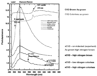
[0043] FIG. 3 shows Photoluminescence (PL) and Raman spectra that were
measured with
488 nm excitation. CVD diamonds showed an obvious nitrogen-vacancy (N-V)
center at 575
nm; the intensity of this band is higher for the brown relative to the
colorless CVD diamonds.
The as-grown brown CVD diamond that had been annealed to colorless possesses a
strong
nitrogen aggregate (H3) center (see S.J. Charles et al., (2004) Physica Status
Solidi (a): 1-13)
at 503 nm with a decrease in the band associated with the N-V center. Note
that the H3 peak
is strongest for the unindented (ultrahard) diamond. The annealed as-grown
colorless CVD
diamond possesses both H3 and N-V centers, but the intensities of these bands
decreased by
two orders after annealing, and the second-order Raman band of diamond
appeared. The N-V
8
CA 02589299 2007-03-07
WO 2007/018555
PCT/US2005/032199
centers in the annealed CVD (aCVD) may imply vacancy-rich CVD transforms to
denser
structures after HPHT annealing.
[0044] FIG. 4 shows the C-H stretching of infrared absorption in the range
of 2800-3200
cm-1. The broad band at 2930 cm-1 attributed to hydrogenated amorphous carbon
(a-C:H) is
observed in the brown CVD diamond. This intensity correlates with the brown
color of the
diamond and its high toughness. As shown in FIG.4, the a-C:H peak was annealed
to various
well-resolved C-H stretching bands at 2830 cm-1 (sp3 {111} defects), 2875 (sp3-
CH3 defects),
and 2900 cm-1 (sp3 {100} defects) as well as 2972, 3032 and 3107 cm-1 (sp2
defects) (see
K.M. McNamaara et al. I Appl. Phys. (1994) 76, 2466-2472). The {111} surfaces
within the
aCVD implies the relatively open a-C:H structure in the as-grown {100} CVD
transformed
on annealing to locally denser structure. For example, there is an increase in
internal
{111}defects and sp2 carbon on the boundary. This change may contribute to the
square
<111> or <110> indented pattern in FIG.2. The colorless CVD diamond has lower
intensity
bands associated with a-C:H exhibited a broad and intense band at 2800 cm-1.
This feature
could be associated with unintentional contamination of boron (see Z. Teukam
et al., Natural
Materials (2003) 2: 482-486), related C-H modes (see K.M. McNamaara et al. I
Appl. Phys.
(1994) 76, 2466-2472) or an unknown center (still under investigation). Ion
microprobe
analysis of the diamond revealed a maximum concentration of the N in the CVD
diamond
was approximately 75 times less than that of the type lb substrate.
[0045] It is important to note that no grain boundaries were optically
observed in aCVD
diamonds. The aCVD crystals do not have obvious nitrogen-related absorption
peaks at
1000-1500 cm-1, even if a small amound of nitrogen is intentionally added to
the synthesis
gas; thus these diamonds may be considered type Ha. Without wishing to be
bound by theory,
it is believed that the mechanism of hardness/toughness enhancement and color
changes in
aCVD diamonds differs from annealed natural or HPHT synthetic diamond where
nitrogen
dominates.
[0046] Examination under crossed polarizers shows this CVD diamond has
relatively high
internal stress in comparison to other diamonds. After HPHT treatment the
stress can be
reduced, but in Ia, lb, Ila diamonds the stress can increase after annealing.
Without wishing to
be bound by theory, it is believed that this phenomenon implies the hardness
enhancement in
9
CA 02589299 2007-03-07
WO 2007/018555
PCT/US2005/032199
annealed IIa may be due to stress-induced dislocation, although further
investigation of this is
needed (see K Kanda, (2003) Diamond Related Matter, 12, 1760-1765).
[0047] Additional information is obtained from measurements of x-ray
rocking curve,
including rocking curve maps. The full width at half-maximum (FWHM) of the
colorless
diamond is ¨20 arcsec, brown CVD is ¨80 arcsec, and aCVD is ¨150-300 arcsec.
Without
wishing to be bound by theory, it is believed that the broadened FWHM in the
aCVD crystal
is likely associated with the a-C:H in CVD transforming to denser diamond
domains with a
fair amount of mosaic spread.
Table 1. Summary of analyses
As-grown PL FTIR at C-H FWHM X-ray
Ultrahard 4% N2/CH4, 113 {111} {100} No data
aCVD brown face, sp2
Superhard 4% N2/CH, Strong Sharp strong 300 arcsec
aCVD Dark brown H3 {111}, {100}
face, sp2
Supertough 0.4% N2/CH4, Weak Boron or 150 arcsec
aCVD colorless N-V, 113 unknown center
[0048] The mechanism of the very high fracture toughness documented here may
be
associated with the small amount of amorphous carbon or dislocations that
exist in these
single-crystal CVD diamonds. Denser sp2 or sp3 hybridized nanocrystals
combined with
changes in nitrogen and hydrogen impurities on their grain boundary may occur
during HPHT
annealing.
[0049] The ultratough diamonds of the invention and diamonds produced by the
above
methods will be sufficiently large, tough, defect free and translucent so as
to be useful as, for
example, windows in high power laser or synchrotron applications, as anvils in
high pressure
apparatuses, as cutting instruments, as wire dies, as components for
electronics (heat sinks,
substrates for electronic devices), or as gems. Other examples of uses or
applications for the
above ultratough diamonds and diamonds made by the above methods include the
following:
CA 02589299 2007-03-07
WO 2007/018555
PCT/US2005/032199
a.) wear resistant material¨including, but not limited to, water/fluid jet
nozzles, razors,
surgical blades, microtone, hardness indentor, graphical tools, stichels,
instruments used in
the repair of lithographic pieces, missile radomes, bearings, including those
used in ultra-high
speed machines, diamond-biomolecule devices, microtomes, and hardness
indentors;
b.) optical parts¨including, but not limited to, optical windows, reflectors,
refractors, lenses,
gratings, etalons, alpha particle detectors, and prims;
c.) electronics¨including, but not limited to, microchannel cooling
assemblies; high purity
SC-CVD diamonds for semiconductor components, SC-CVD doped with impurities for
semiconductor components
d.) anvils in high pressure apparatuses¨including, but not limited to, the
"Khvostantsev" or
"Paris-Edinburgh" toroid shaped anvils that can be used with multiple optical,
electrical,
magnetic, and acoustic sensors; Bridgman anvils that are relatively large,
have variable
heights, and include major angles [15]; Multianviles, Drickamer cells, belt
apparatus, piston-
cylinder apparatus; precompressing samples for laser or magnetic shock wave
studies;
colorless, smooth coating for hydrogen and other applications, apparatus for
pre-compressing
samples for lasers or magnetic shock;
e.) containers¨including, but not limited to, 6 edge {100} plated diamonds can
be connected
to each other to form a container, CVD diamond coating can be further employed
to form a
vacuum tight container;
f.) laser source-including, but not limited to, annealing SC-CVD diamond to
form a stable
H3 center (nitrogen aggregate, N-V center, Si center, or other dopants;
g.) superconductor and conducting diamond¨including, but not limited to, HPHT
annealing
with SC-CVD diamond grown with an impurity such as H, Li, N, Mg, or another
low atomic
weight element with a size approaching that of carbon;
h.) substrate for other CVD diamond growth¨using CVD plates as substrates for
CVD
growth has the advantage over natural or HPT substrates in large size and
toughness (to avoid
cracking during growth).
[0050] The ultratough diamonds disclosed herein are particularly useful in
applications,
including, but not limited to, water/fluid jet nozzles, razors, surgical
blades, microtone,
hardness indentor, graphical tools, stichels, instruments used in the repair
of lithographic
pieces, missile radomes, bearings, including those used in ultra-high speed
machines,
11
CA 02589299 2011-12-23
diamond-biomolecule devices, microtomes, hardness indentors, and anvils in
high pressure
apparatuses.
[0051] In one embodiment, the present invention is directed to anvils in
high pressure
apparatuses, wherein the anvils comprise ultratough single-crystal CVD
diamond. Anvils
comprising ultratough single-crystal CVD diamond can be used at higher
pressures than
anvils made of other materials, such as tungsten carbide. Examples of anvil
designs that can
comprise single crystal CVD diamonds include Bridgman anvils, including, but
not limited
to, Bridgman anvils that are relatively large, include variable heights, and
include major
angles and Paris-Edinburgh toroid anvils, including, but not limited to, those
discussed in
Khvostantsev, L.G., Vereshchagin, L.F., and Novikov, A.P., Device of toroid
type for high
pressure generation, High Temperatures ¨ High Pressures, 1977, vol. 9, pp 637-
638.
[0052] In another embodiment, the present invention is directed to an
ultratough single-
crystal CVD diamond that is laser inscribed with identifying marks (e.g.,
name, date, number)
and a method of preparing such a diamond. The, identifying marks can be laser
inscribed onto
a diamond substrate prior to starting the CVD process to prepare a single-
crystal diamond.
The mark is transferred to the single-crystal diamond through this process.
[0053] As the present invention may be embodied in several forms without
departing from
the spirit or essential characteristics thereof, it should also be understood
that the above-
described embodiments are not limited by any of the details of the foregoing
description,
unless otherwise specified, but rather should be construed within the spirit
and scope
defined in the appended claims.
12