Note: Descriptions are shown in the official language in which they were submitted.
CA 02589485 2007-05-28
WO 2006/063081 PCT/US2005/044319
MINIATURE CIRCUITRY AND INDUCTIVE COMPONENTS AND
METHODS FOR MANUFACTURING SAME
This application claims the benefit of U.S. Provisional Application No.
60/633,742
filed December 7, 2004 the entire contents of which is expressly incorporated
herein by
reference.
Field of the Invention
[00011 The present invention relates to improvements in miniature electrical
circuits and inductors and transformers and methods of manufacturing these
devices.
Summary of the Invention
[0002] One aspect of the invention is a high yield process for manufacturing
improved miniature circuits, inductors and transformers having high functional
reliability. In
particular, the process fabricates two or more independent and isolated
conductors in the
same via holes. Aspects of this embodiment include closely spacing while
maintaining a
high voltage barrier between the conductors and providing interconnect
reliability.
[0003] For inductive embodiments, the two or more independent conductors are
advantageously fabricated on the wall of a hole either in or proximate to a
ferrite member
embedded in a cavity in a printed circuit board or flexible circuit.
Embodiments include
holes located in a ferrite plate and holes located around a ferrite toroid.
These conductors
function as windings of an inductor or transformer.
[0004] In another embodiment, the two or more independent conductors are
foimed on the wall of vias in circuit board or flexible circuits to
interconnect circuits and
circuit elements located on opposite sides of the printed circuit board or
flexible circuit.
[0005] Extremely miniature devices are constructed by providing an extremely
thin but very high dielectric film between plural plated through hole
conductors in each via.
hi addition, further miniaturization is provided by utilizing printed circuits
over the entire
surface of the support panel and locating surface mounted components over the
magnetic
members embedded within the support panel.
CA 02589485 2007-05-28
WO 2006/063081 PCT/US2005/044319
[0006] The miniaturization achieved by the circuits and processes enable, for
example, very sinall and lightweight power supplies for laptop computers,
digital cameras,
portable audio and T.V. devices, and cell phones.
[0007] The improved inductor and circuit configurations enable efficient and
repeatable manufacture of miniature circuits and miniature inductors and
transformers having
high voltage, high current capabilities, as well as high tolerance to physical
stress.
Brief Description of the Drawinys
[0008] Figure 1 is a perspective view illustrating a support panel with a
plurality
of toroidal cavity openings routed therein;
[0009] Figure 2A is a perspective view illustrating embedded ferrite toroids
in
each of the routed cavity openings in the support plate;
[0010] Figure 2B is a cross-sectional view along lines 2B-2B of Figure 2A;
[0011] Figure 3 is a cross-sectional view of the support panel having copper
layers on opposite sides;
[0012] Figure 4 illustrates a cavity and the removal of the top copper layer
fiom
the support panel;
[0013] Figure 5 is a cross-sectional'view illustrating the lay-up prepreg
rings and
prepreg copper foil lamination;
[0014] Figure 6 is a perspective view of the toroid ferrite;
[0015] Figure 7 is a cross-sectional view showing the assembly prior to the
lamination of the copper foil;
[0016] Figure 8 is a cross-sectional view showing the assembly after
lamination
of the copper foil;
[0017] Figure 9 is a top elevational view showing the through via holes formed
around the outer and inner walls of the ferrite core;
[0018] Figure 10 is a cross-sectional view of the via holes;
[0019] Figure 11 is a cross-sectional view illustrating copper plating of the
assembly;
[0020] Figure 12A is a top elevational view showing the first layer of printed
circuit conductors;
-2-
CA 02589485 2007-05-28
WO 2006/063081 PCT/US2005/044319
[0021] Figure 12B is a bottom elevation view showing the second layer printed
circuit conductors;
[0022] Figure 13 is a cross-sectional view showing application of the first
insulating layer over the first and second layers of printed circuit and over
the first plated
through hole;
[0023] Figure 14 is a cross-sectional view showing the application of the
second
insulating layer;
[0024] Figure 15 is a cross-sectional view showing the application of the
third
iiisulation layer and adhesion promotor;
[0025] Figure 16 is a cross-sectional view illustrating the lay-up of
predrilled
bond ply and copper foils;
[0026] Figure 17 is a cross-sectional view showing the assembly after
lamination
of the copper foils;
[0027] Figure 18 is a cross-sectional view showing transformer via holes
etched
from the copper foils;
[0028] Figure 19 is a cross-sectional view showing the copper plating over the
assembly;
[0029] Figure 20 is a cross-sectional view illustrating the lay-up prepreg and
copper foil before lamination;
[0030] Figure 21 is a cross-sectional view illustrating the laminated
assembly;
[0031] Figure 22 is a cross-sectional view illustrating the application of a
cover
layer or solder mask to the assembly;
[0032] Figure 23 is a perspective view of a power supply in which the
inductive
elements are embedded in the printed circuit panel;
[0033] Figure 24 is a perspective view of another embodiment having a support
panel having a plurality of rectangular openings;
[0034] Figure 25 is a perspective view illustrating a support panel having
rectangular ferrite plates in each of the openings;
[0035] Figure 26 is a cross-sectional view of an embodiment utilizing
rectangular
ferrite plates;
-3-
CA 02589485 2007-05-28
WO 2006/063081 PCT/US2005/044319
[0036] Figure 27 is an elevation view of a subassembly illustrating the
transparency of the parylene insulating layer;
[0037] Figure 28 is a photomicrographic view of an exemplary cross-section
showing two parylene insulated conductive vias in a single via hole as formed
by this
invention;
[0038] Figure 29 is a photomicrographic view of an exemplary cross-section
showing three parylene insulated conductive vias in a single via hole as
formed by this
invention; and
[0039] Figure 30 is a photomicrographic view of an exemplary cross-section
showing four insulated conductor vias in a single via hole as formed by this
invention.
[0040] Figure 3 1A is an elevational view of the first or top printed circuit
level of
another embodiment having two toroids embedded into the support panel;
[0041] Figure 31B is an elevational view of the second or bottom printed
circuit
level of the embodiment of Figure 3 1A;
[0042] Figure 32A is an elevational view of the third printed circuit level,
of the
embodiment of Figure 31A, formed in a plane proximate to and over the plane of
the first
printed circuit layer;
[0043] Figure 32B is the elevational view of fourth printed circuit level
formed in
a plane proximate to and over the plane of the second printed circuit level of
Figure 31B;
[0044] Figure 33A is an elevational view of the fifth printed circuit level of
the
embodiment of Figure 31A, formed in a plane proximate to and over the plane of
the third
printed circuit level of Figure 32A;
[0045] Figure 33B is an elevational view of the sixth printed circuit level of
the
embodiment of Figure 31A proximate to and over the plane of the fourth printed
circuit level
of Figure 32B;
[0046] Figure 34A and 34B are perspective views of the top and bottom of a
power supply constructed utilizing the printed circuit level shown in Figures
3 1A, 31B, 32A,
32B, and 33A, 33b;
-4-
CA 02589485 2007-05-28
WO 2006/063081 PCT/US2005/044319
[0047] Figure 35 is a cross-sectional view illustrating the use of the plated
through
holes for both forming winding turns for conductors and transformers and for
providing
electrical connections between other printed circuitry layers.
Detailed Description of the Preferred Embodiments
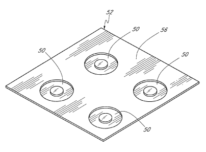
[0048] The process for manufacturing one embodiment of inductive component
devices is illustrated in Figures 1-22. As shown in Figure 1, a plurality of
toroidal openings
or cavities 50 are formed, typically by routing, in a support panel 52. Panel
52 is
advantageously an FR-4 epoxy laminate sheet 54 with copper layers 56, 58 on
opposite sides,
as shown in Figure 3, although it will be apparent that sheets made from other
materials
including other types of sheets used for circuit board fabrication and rigid
flex are applicable
for use as support panel 52. Using standard techniques of printed circuitry,
the top copper
layer 56 is then eliminated using the dry film to mask the bottom surface of
the support panel.
The exposed (unmasked) copper layer 56 is then etched off from the top
surfaces of the
panel. The remaining dry fihn mask is then stripped from the bottom surface to
provide a
support panel having the cross-section shown in Figure 4.
[0049] Figures 1 and 2A illustrate a support panel 52 on which four cavities
are
formed to simultaneously manufacture four inductor or four transformer
components after
which the support board is cut or mounted to produce a plurality of individual
components
such as illustrated in Figures 23, 34A, and 34B. It will be understood that
the processes
described below are usually used to simultaneously manufacture a larger number
of
components, typically in the range of 16 to 20 components. Also, each
component may
include a single cavity embedding a single magnetic toroid or may include two
or more such
cavities and toroids to produce two or more embedded inductive devices for a
particular
electronic device. See, e.g., the power supply described below and shown in
Figures 34A and
34B.
[0050] Following the cavity preparation, one or more prepreg toroidal rings 60
are
seated onto the bottom of each of the formed toroidal openings 50 as shown in
Figure 5.
[0051] Ferrite toroids 62 (shown in Figure 6), are then respectively embedded
within the openings 50, as shown in Figures 2A and 2B. Each of these ferrite
toroids 62
serve as a ferromagnetic slab for a fabricated inductive component. By way of
specific
-5-
CA 02589485 2007-05-28
WO 2006/063081 PCT/US2005/044319
example, the toroid may have an outside diameter of 1.25 inches and an opening
of 3/8
inches. A copper foil 70, is then laminated to the top surfaces of the ferrite
toroid 62 using an
epoxy prepreg 72 or other suitable adhesive to affix the foil to the ferrite
plate. Depending
upon the ultimate application of the inductive component, the copper foil will
typically also
cover all or part of the support panel 52.
[0052] The lay-up of the prepreg rings 60, ferrite toroids 62 and lay-up
prepreg 63
and copper foi170 is illustrated in Figure 5. The laid-up subassembly is shown
in Figure 7A.
[0053] As illustrated in Figure 7B, panel 52 and assembled ferrite toroids,
prepreg
and copper foil are then placed in a holding fixture of a laminating machine
(not shown) that
applies pressure and heat resulting in the top surfaces of the ferrite cores
62 being made
substantially flush with the top surfaces of board 52 and prepreg material
filling the voids
between the walls of openings 50 and ferrite cores as well as laminating the
copper foi170
over the cores 62 and support pane152 as shown in Figure S. The resultant flat
surface over
the embedded toroid ferrite permits multiple additional circuit layers and
mounting of circuit
elements over the entire support panel 56. As described below, extremely small
components
such as switching power supplies and battery chargers for laptops, conlputers,
digital
cameras, cell phones, portable audio and TV's and the like can be constructed.
[0054] In this lamination step and the lamination steps described below, the
materials used are selected to provide the desired physical properties for the
finished
circuitry. These properties are commonly referred to as peel strengths and
bond strengths.
The preferred materials for laminating are: Medium or High Tg epoxy prepregs
from LG,
Isola, Polyclad or Arisawa.
[0055] Through holes (vias) 80 and 81 are then respectively drilled through
the
laminated subassembly pane185 around the outside and inside of ferrite toroids
using
conventional drilling equipment. These via holes are typically 12 to 50 mils
in diameter. As
described below, these through holes or vias 80 and 81 (shown in Figures 9 and
10) enable
fabrication of plated through hole conductors wlzich function as electrical
windings for the
inductor or transformer device.
[0056] After drilling, the laminated panel 85 is advantageously plasma etched
to
clean the drilled holes. This step is advantageously followed by a glass etch
to remove
-6-
CA 02589485 2007-05-28
WO 2006/063081 PCT/US2005/044319
spurious glass particles from the holes 80, 81 or roughen the glass fibre for
adhesion of the
copper plating followed by chemically cleaning the vias 80, 81 and the top and
bottom
surfaces of the exposed copper sheets 58 and 70.
[0057] A conventional process is then used to chemically coat the inside
surface
of all of the through holes 80, 81. In one en7bodiment, the SHADOW process is
utilized.
Other processes include an electroles copper deposition and DMSE/HDI process.
[0058] Following this application of the chemical coating, the subassembly 85
is
copper plated. The plated copper 90 is shown in Figure 11 and covers both the
copper foil
laminate 58, the copper foil laminate 70 and the internal walls of the through
holes (vias) 80,
81 (shown at 95) so as to electrically connect the top and bottom copper foils
58, 70 via the
plated through holes 95.
[0059] Printed circuits 100, 101 (shown in Figures 12A and 12B) are then
fabricated using the top and bottom layers' of the copper laminate 58, 70 and
plated
copper 90. These circuits 100, 101 are advantageously formed by vacuum
laminating a dry
photographically developable film over the surfaces of the plated copper on
the top and
bottom of the subassembly. Using standard, well known techniques of printed
circuitry, first
layer 100 and second layer 101 of circuitry are fabricated by using the dry
film to mask the
desired circuitry. The exposed, i.e., unmasked copper is then etched from both
top and
bottom surfaces of the component assembly. The remaining dry film mask is then
stripped
from those top and bottom surfaces. The remaining copper forms a first layer
of circuitry 100
on the top surface (shown in Figure 12A), and a second layer of circuitry 101
(shown in
Figure 12B) on the bottom surface, interconnected by the copper plated via
holes 95. As
described below, these formed printed circuits respectively include circuits
100, 101 which
are respectively connected at each end to a plated through hole 80, 81 to
provide a
continuous, electrical winding around the ferrite core encased in the support
member. These
windings and feiTite core fomi a miniature inductor transformer.
[0060] The top and bottom surfaces are then chemically cleaned. The component
assenzbly is then vacuum baked to remove any remaining moisture.
[0061] The component assembly is then prepared for an additional copper layer
and an additional plated via insulated from but fabricated over the first
copper layers. An
-7-
CA 02589485 2007-05-28
WO 2006/063081 PCT/US2005/044319
insulating coating is used to separate the multiple layers of circuitry and
plated vias. Epoxy,
polymer, liquid polyamide and other materials may be used. However, parylene
coating has
been discovered to be particularly advantageous for forming these insulating
layers. Parylene
is an organic coating with an inert surface. In one embodiment, in preparation
for the
parylene coating, an adhesive promotor such as a very thin Silane, Carboxyl or
Silane and
Carboxyl layer 110 (shown in Figure 13) is deposited on the subassembly
including the top
and bottom surfaces and walls of the plated through holes using a PECVD
process (Plasma
Enhanced Chemical Vapor Deposition) or other suitable process. In another
embodiment,
this very thin layer 110 may be formed by dipping the subassembly in a Silane
or other
adhesive before deposition of the parylene.
[0062] The parylene is then vacuum deposited over the entire subassembly to
leave, as illustrated in Figure 14, a thin coating 1.15 over the first (top)
layer of circuitry 100,
a thin coating 116 over the second (bottom) layer of circuitry 101 and a thin
coating 117 over
(inside) the copper plated through hole 95.
[0063] This parylene coating is pinhole free and has a high dielectric
strengtli with
veiy thin coatings providing very high voltage breakdown values. By way of
specific
example, parylene coatings formed of Parylene C with thicknesses of .0005 mil
to .001 mil
provide a voltage breakdown guard band of about 5600 volts per mil of
thickness.
Parylene C has a dielectric constant of about 2.28.
[0064] Nova HT Parylene provides an even higher dielectric constant of about
3.15 and provides a voltage breakdown of about 750 volts per micron of
thickness. As a
result, very thin coatings, e.g. 10 to 15 microns provides a brealcdown
voltage barrier in the
range of 7500 volts or higher.
[0065] A parylene coated subassembly is shown in Figure 27. This and other
parylene coatings shown in other photographs were coated at the SCS Coating
Center at
Ontario, California.
[0066] The thickness of the deposited parylene layers 115, 116 and 117 is
determined by several factors including physical size of the manufactured
inductor or
transformer, physical size of the through hole openings 80, 81, the number of
insulated
plated through hole conductors to be formed in a through hole, and the power
rating of the
-8-
CA 02589485 2007-05-28
WO 2006/063081 PCT/US2005/044319
manufactured product. For the miniature inductors and transformers described
below, the
thickness of the parylene layer will be in the range of about .5 mil to 3
mils. (.0005 to .003
inches), and the brealcdown guard band will be in the range of about 5600 to
15,000 volts per
mil of thickness of the parylene layers.
[0067] The extremely thin parylene provides a high dielectric coating between
the
copper plated through holes and enables plural such through hole conductors to
be formed in
a very small through hole opening. A furtlier aspect of the these coatings
that enables =
multiple conductors through a single very small via is that the vacuum
deposited parylene
provides a substantially uniform thickness coating that closely follows the
contour of the
underlying copper plate. As a result, the parylene does not, of itself, cause
an unpredictable
build up of thickness in the plated through hole. The diameter of the through
holes will
typically be determined by the thickness of the support panel 56 and the
number of plated,
through holes to be formed in each through hole. The panel thickness is
typically in the range
of about 62 mil to 15 mil. Typically the hole size will range from about 12
mil to 50 mil.
For a panel 90 mil thick, a hole size of about 22 mil diameter will typically
be used to form
two plated through holes within this through hole and a hole size of about 40
mil diameter
will be selected to form four plated through holes. For a thicker panel .125
mil thick, a hole
size of about 28 mil would typically be used to form two plated through holes
and a hole size
of about 40 to 60 mil will typically be used to form four plated tlirough
holes.
[0068] While having excellent dielectric insulative properties, the surface of
the
deposited parylene will not bond or adhere to plated copper. It has been
discovered,
however, that a suitable adhesive promoter is accomplished by adding a
positively charged
moiety to the baclcbone of the parylene compound. This is advantageously
accomplished by
using the plasma enhanced chemical vapor deposition (PECVD) process. In one
embodiment, the process is a Carboxl or Silane gas phase chemical reactions at
low pressures
(10 to 500 mT), voltages typically in the range of about 200 to 700 volts,
currents typically in
the range of about 3 to 7 amp and power in the range of about 6V to 2000
watts. The
resulting surface (indicated at 120 in Figure 15) populated with reactive
sites, ready to receive
an adhesive or coating. The mechanism is believed to be primarily due to
hydrogen bonding
and covalent bonding due to this adhesive or coating reacting to the changed
moiety.
-9-
CA 02589485 2007-05-28
WO 2006/063081 PCT/US2005/044319
[0069] Formation of third and fourth layers of circuitry begins with drilling
hole
openings 122, 123 in adhesive sheets 125, 126 before these sheets are
positioned onto the
assembly. These openings 122, 123 are drilled to register over the first and
second layer
circuitry openings 80, 81. As shown in Figure 16, the pre-drilled adhesive
sheets 125 and
126 are then respectively positioned over the top and bottom surfaces of the
subassembly. A
low temperature lamination process is then used to partially laminate the pre-
drilled adhesive
sheet 125, to the surface of the parylene coated top surface of this top
circuitry layer 100 and
adhesive sheet 126 to the surface of the parylene coated bottom circuitry
layer 101, as shown
in Figure 12B. Copper foil 130, is then attached to the top side of the
adhesive coated panel
and copper foil 131 is attached to the bottom side of the adhesive coated
panel.
[0070] Copper foils 130, 131 are then' laminated to the subassembly at high
ten7perature and pressure to form a four copper layer assembly shown in Figure
17 with the
third layer 130 and the fourth layer 131, respectively, insulated from the
circuitry layers 100,
101 by the insulating layers 110, 115, 116, 120.
[0071] Using the well known techniques of printed circuitry, via holes 135,
136,
137, and 138 (shown in Figure 18) are formed:in the copper foils 130, 131 by
using the dry
film to mask the copper. The unmasked copper is then etched fiom both top and
bottom
surfaces of the component assembly to form these vias 135-138. The remaining
dry film
mask is then stripped fiom those top and bottom surfaces.
[0072] The surfaces of copper foils 130, 131 are now chemically coated using
the
SHADOW process. Following the application of a chemical coating using the
SHADOW
process, the subassembly is again copper plated. The plated copper 145 is
shown in Figure
19 and covers both the copper foil laminate 130, copper foil laminate 131 and
the parylene
coated walls of the plated through holes 95 so as to form second conductive
through holes
140 in the same through hole and thereby electrically connect the third and
fourth copper
plated foils 130, 131.
[0073] Third and fourth printed circuits 150, 151 are then fabricated using
the top
and bottom layers of plated copper foils 130, 131. These circuits are
advantageously formed
by vacuum laminating a dry photographically developable film over the top and
bottom
surfaces of the plated copper. Using standard well known techniques of printed
circuitry,
-10-
CA 02589485 2007-05-28
WO 2006/063081 PCT/US2005/044319
these third and fourth layers of circuitry are fabricated by using the dry
film to mask the
desired circuitry. The exposed (unmasked) copper is then etched from both top
and bottom
surfaces of the component assembly. The remaining dry film mask is then
stripped from
those top and bottom surfaces. The remaining copper forms the desired third
layer of
circuitry 150 on the top surface, the fourth layer of circuitry 151 on the
bottom surface, and
the circuitry connections between layers 150, 151 provided by the copper
plated via
holes 140.
[0074] The top and bottom surfaces are then chemically cleaned. The component
assembly is then vacuuin balced to remove any remaining surface chemicals.
[0075] Additional fifth and sixth layers of circuitry 160, 161 are fabricated
over
the third and fourth layers. In the embodiment shown in Figure 20, these
circuit layers are
insulated from the adjacent third and fourth layers by two layers of prepreg
165. By way of
example, the Isola medium Tg epoxy prepreg has a voltage brealcdown rating of
1100 to 1200
volts per mil thickness. By way of specific example, a 4 mil thickness of this
prepreg was
used to provide a voltage breakdown of over 4000 volts. These fifth and sixth
circuit layers
are formed following the cleaning and baking steps as follows:
1) Drill the fifth layer 160 and sixth layer 161 copper foils with tooling
holes
2) Drill tooling holes in two sheets of adhesive, or prepreg
3) Lay up two additional adhesive coated copper foils 160, 161, or copper foil
and prepreg on to the asseinbly shown in Figure 19 containing four layers of
circuits
4) Laminate all the material together at high temperature and pressure using a
vacuum lamination process so the result at this stage of manufacture is an
assembly shown in Figure 21 having six copper foil layers 58, 70, 130, 131,
160 and 161 with circuit layers 58 and 70 interconnected via the plated holes
95 and circuit layers 130 and 131 interconnected by plated holes 140 which
are isolated from the plated holes 95 but using the same via holes
5) As shown in Figure 35, additional through holes 153 may now be selectively
drilled through the respective plated copper sheets and support panel 56 to
enable, for example, through hole cozmectors for surface mounted circuit
-11-
CA 02589485 2007-05-28
WO 2006/063081 PCT/US2005/044319
elements, e.g., semiconductors, capacitors, resistors located over the cavity
50
and embedded toroid 62 as shown in Figures 34A and 34B.
6) Plasma etch
7) Glass etch
8) Chemical clean the surfaces of layers 160 and 161
9) Shadow Process the surfaces of the interconnecting holes
10) Copper plate the surfaces and the holes
11) Chemical clean
12) Vacuum laminate dry film
13) Expose the fifth and sixth circuit layers 160, 161 for etching
14) Etcll the fifth and sixth circuitry layers 160, 161 to form printed
circuits from
the plated foils 160, 161
15) Strip dry film from surface of the fifth and sixth layers of printed
circuitry
16) Chemical Clean
17) Vacuum bake
18) Laminate two covercoats or apply cover layers or solder masks 170, 171
over
the fifth and sixth printed circuit layers (as shown in Figure 22) while
including appropriate openings to accommodate components to be assembled
there-on
19) Bright tin/lead plate or apply protective coating onto the exposed copper
circuitry underneath the covercoat openings
20) Separate each individual assembly by routing or cutting apart the
individual
rectangular circuits each containing an embedded individual ferrite toroids
and six circuitry layers
21) Test
22) Assemble electrical circuit elements onto the individual miniature
inductor or
transformer components as shown in Figure 23 and 34A, 34B
23) Test the final assembly
-12-
CA 02589485 2007-05-28
WO 2006/063081 PCT/US2005/044319
[0076] The assembly described above and shown in Figure 23 has six layers of
printed circuitry and two plated through holes 95 and 120 through each hole
(via) 80, 81
formed in the support pane156 around the outside and inside of the embedded
toroidal ferrite.
In the assembly shown, the first, second, third and fourth printed circuitry
layers and plated
through holes 95 and 120 form circuitry and the windings of an inductor or
transformer.
[0077] By way of specific example, Figure 23 illustrates an embodiment of a
miniature power supply 195 constructed in accordance with this invention. As
shown, the
magnetic components of the power supply are entirely encapsulated within the
printed circuit
board. By way of specific example, the support panel for this embodiment has a
length of
2 3/16 inches and a width of 1 13/16 inches.
[0078] In the foregoing embodiment, ferrite toroids are used to form inductors
and transformers in the plane of the circuit board or flexible circuit. It
will be understood that
other types of magnetic or ferrite configurations may be utilized, such as
oval shaped toroidal
ferrite structures and ferrite slabs having various geometric configurations
or other magnetic
materials. In other embodiments, the through hole conductors are formed by
processes other
than copper plating, instead utilizing, for example, conductive pastes. In
addition, the plural
plated through holes insulated from each other may be formed directly through
the magnetic
material. Construction of such another embodiment of the invention is shown in
Figures 24-
26. In this embodiment, the manufacture of a multiple through hole assembly
utilizes a slab
of ferrite material and vias drilled are formed through the ferrite slab.
Plural conductive
through holes are formed in each via.
[0079] As shown in Figure 24, a plurality of rectangular openings 200 are
formed
typically by routing, in a support panel 205. Panel 205 is advantageously an
FR-4 epoxy
laminate sheet although it will be apparent that sheets made from other
materials including
other types of sheets used for circuit board fabrication are applicable for
use as support panel
205. In this embodiment, the openings are formed completely through the
support panel.
[0080] Ferrite plates 210 are respectively embedded within the openings 200,
as
shown in Figure 25. Each of these ferrite plates"210 serve as a ferromagnetic
slab on which
is fabricated inductive components. As described below, these plates 210 may
be formed as
shown in Figure 25 without through holes which are subsequently drilled during
construction
-13-
CA 02589485 2007-05-28
WO 2006/063081 PCT/US2005/044319
of the component. In other embodiments a plurality of through holes, as seen
in Figure 27,
may be pre-formed during molding of ferrite slabs.
[0081] The ferrite plate 210 is shown in cross-section in Figure 26. This
figure
shows the surface of the ferrite plate 210 including the walls of its through
hole openings 215
covered with an insulating layer 220. Advantageously, this layer is formed by
a vacuum
deposited parylene coating as described in detail above. Layer 220 insulates
the ferrite
material from the copper circuitry to be fabricated over the ferrite surface
and on the walls of
the through holes in the ferrites. This coating is advisable or necessary for
low resistivity
ferrites, e.g., high permeability ferrites of the order of 2300 PERM. Coating
220 will often
not be utilized for lower permeability ferrites, such as 350 PERM ferrites
having a higher
resistivity.
[0082] Copper foils 225, 226 are then respectively laminated to the top and
bottom surfaces of the ferrite plate 210 using an epoxy prepreg 230 or other
suitable adhesive
to affix the foil to the ferrite plate. Depending upon the ultimate
application of the inductive
component, the copper foil will typically also cover all or part of the
support panel 205. In
this lamination step and the lamination steps described below, the materials
used are selected
to provide the desired physical properties for the finished circuitry. These
properties are
commonly referred to as peel strengths and bond strengths. The preferred
materials for
laminating are: Crystal, B-1000, R1500 from Rogers Corp., Pyralux FB from
Dupont, CA
338, CA 333, E33 from Shin-Etsu, AY50KA, CY2535KA, CVK2,530130, SAU, SPC, SPA
from Arisawa, and Medium or High Tg epoxy prepregs from Isola.
[0083] Through holes or vias 215 in the ferrite plates 210 (shown in Figures
26
and 27) enable fabrication of plated through conductors. These plated through
vias function
as electrical windings for the inductor or transformer device. These holes are
typically 12 to
50 mil in diameter but can be larger or smaller, (e.g., as small as 4 mil in
dian7eter) depending
upon the specifications of the inductor or transformer being manufactured. In
some
embodiments, the ferrite plates are molded or otherwise pre-formed with the
desired through
holes 215. In such embodiments, through holes using conventional drilling
equipment are
drilled through the copper foil after the foil is laminated to the ferrite
plate 210. These holes
are drilled so as to register with the preformed holes in the ferrite plates.
In otlzer
-14-
CA 02589485 2007-05-28
WO 2006/063081 PCT/US2005/044319
embodiments, such as the ferrite plates 210 shown as Figure 215, the ferrite
plates are not
pre-formed with holes. In these embodiments, the holes are formed in the
ferrite plates 210
after lamination of the copper foils 225, 226. Drilling holes through the
ferrite plates and
copper foil is advantageously performed using laser drilling equipment.
[0084] After drilling, the laminated panels are advantageously plasma etched
to
clean the drilled holes. This step is advantageously followed by a glass etch
to remove
spurious glass particles from the holes 215 followed by chemically cleaning
the top and
bottom surfaces of the exposed copper.
[0085] A conventional process is then used to chemically coat (shown at 245)
the
top and bottom surfaces of the copper foil in preparation of copper plating
these top and
bottom surfaces as well as the inside surface of all of the through holes 215.
This process is
commonly referred to as the SHADOW process.
[0086] Following the application of the chemical coating 245 using the
SHADOW process, the subassembly is copper plated. The plated copper is shown
in Figure
26 and covers both the copper foil laminate 225, the copper foil laminate 226
and the internal
walls of the through holes (vias) 215 (shown at 230) so as to electrically
connect the top and
bottom copper foils 225, 226 via the plated through holes 230.
[0087] Printed circuits are then fabricated using the top and bottom layers of
copper laminate and plated copper. These circuits are advantageously formed by
vacuum
laminating a dry photographically developable film over the surfaces of the
plated copper on
the top and bottom of the subassenlbly.
[0088] Using standard techniques of printed circuitry, first and second layers
of
circuitry are fabricated by using the dry film to mask the desired circuitry.
The unmasked
copper is then etched from both top and bottom surfaces of the component
assembly. The
remaining dry film mask is then stripped from those top and bottom surfaces.
The remaining
copper forms a first layer of circuitry 250 on the top surface, as shown in
Figure 26, and a
second layer of circuitry 251 on the bottom surface, interconnected by the
copper plate via
holes 230.
[0089] The top and bottom surfaces are then chemically cleaned. The component
assembly is then vacuum baked to remove any remaining surface chemicals or
moisture.
-15-
CA 02589485 2007-05-28
WO 2006/063081 PCT/US2005/044319
[0090] The component assembly is then prepared for an additional copper layer
and an additional plated via insulated from but fabricated over the first
copper layers. An
insulating coating is used to separate the multiple layers of circuitry and
plated vias. Epoxy,
parylene, liquid polymide and other materials may be used. However, as
described above,
parylene coating has been discovered to be particularly advantageous for
foiming these
insulating layers. In this process, the parylene is vacuum deposited over the
entire
subassembly to leave, as illustrated in Figure 26, a thin coating 270 over the
top layer of
circuitYy 250, a thin coating 271 over the bottom layer of circuitry 251 and a
thin coating 272
inside the copper plated through hole 230.
[0091] In preparation for parylene coating, a very thin Silane and/or Carboxyl
layer is deposited on the subassembly using a PECVD process (Plasma Enhanced
Chemical
Vapor Deposition).
[0092] This parylene coating is pinhole free and has a high dielectric
strength with
very thin coatings providing very high voltage breakdown values. By way of
specific
example, parylene coatings formed of Parylene C with thicknesses of .0005 mil
to .001 mil
provide a voltage breakdown guard band of about 5600 volts per mil of
thickness. Parylene
C has a dielectric constant of about 2.28.
[0093] Nova HT Parylene provides an even higher dielectric constant of about
3.15 and provides a voltage breakdown of about 750 volts per micron of
thickness. As a
result, very thin coatings, e.g., 10 to 15 microns provides a breakdown
voltage barrier in the
range of 7500 volts or higher.
[0094] One embodiment of the parylene coated subassembly is shown in Figure
27. This and other parylene coatings shown in other photographs were coated at
the SCS
Coating Center at Ontario, California.
[0095] Following application of the parylene coating, this subassembly is
plasma
burned in preparation for additional layers of circuitry over in the top
circuit layers and
bottom layer 250, 251.
[0096] Fornnation of third and fourth layers of circuitry begins with drilling
hole
openings in copper foil sheets 280, 281 that will register over the circuitry
openings shown in
Figure 26. Similar openings registering with these through hole openings are
drilled in two
-16-
CA 02589485 2007-05-28
WO 2006/063081 PCT/US2005/044319
sheets of adliesive 285, 286. A low temperature lamination process is then
used to partially
laminate the pre-drilled copper foils 80, 81 to the pre-drilled adhesives so
that the respective
openings are aligned as shown in Figure 26. The adhesive coated copper foil
280 is then
attached to the surface of the parylene coated top surface of this first
circuitry layer 250 and
the adhesive coated copper foil 281 is attached to the surface of the parylene
coated second
circuitry layer 261.
[0097] Copper foils 280, 281 are then laminated to the subassembly at high
temperature and pressure to form a four copper layer assembly with the third
layer 280 and
the fourth layer 281, respectively, insulated from the circuitry layers 2 by
the respective
parylene coating layers 270, 271.
[0098] The surfaces of copper foils 280, 281 are now chemically coated using
the
SHADOW process. Following the application of a chemical coating using the
SHADOW
process, the subassembly is again copper plated: The plated copper is shown in
Figure 26
and covers both the copper foil laminate 280 (as shown at 290), copper foil
laminate 281 (as
shown at 291) and the parylene coated walls of the plated through holes (vies)
230 (shown at
300) so as to electrically connect the third and fourth copper plated foils
280, 281 via plated
through holes 300.
[0099] Third and foui-th printed circuits are then fabricated using the top
and
bottom layers of plated copper foils 280, 281. These circuits are
advantageously formed by
vacuuin laminating a dry photographically developable film over the top and
bottom surfaces
280, 281 of the plated copper.
[0100] Using the well kiiown conventional techniques of printed circuitry,
these
third and fourtli layers of circuitry are fabricated by using the dry film to
mask the desired
circuitry. The exposed, i.e., unmasked copper is then etched from both top and
bottom
surfaces of the component assembly. The remaining dry film mask is then
stripped from
those top and bottom surfaces. The remaining copper forms the desired third
layer of
circuitry on the top surface, the fourth layer of circuitry on the bottom
surface, and the
circuitry connections between the third and fourth layers connected to the
copper plated via
holes 300.
-17-
CA 02589485 2007-05-28
WO 2006/063081 PCT/US2005/044319
[01011 The top and bottom surfaces are then chemically cleaned. The component
assembly is then vacuum baked to remove any remaining surface chemicals.
[0102] Additional through hole connection holes may now be selectively drilled
through the respective copper sheets and panel 205 to enable, for example,
through hole
connections for the circuit elements located over the ferrite plate 210.
[0103] Additional fifth and sixth layers of circuitry 305, 306 are fabricated
over
the third and fourth layers. In the embodiment shown in Figure 7, these
circuit layers are
insulated from the adjacent third and fourth layers by a relatively thick
single or two or more
layers of prepreg 310. By way of example, the Isola medium Tg epoxy prepreg
has a voltage
breakdown rating of 1100 to 1200 volts per mil thickness. By way of specific
example, a 4
mil thickness of this prepreg was used to provide a voltage breakdown of over
4000 volts.
These fifth and sixth layers are fomied following the cleaning and baking
steps as follows:
1) Drill the fifth and sixth layer copper foils with tooling holes
2) Drill tooling holes in two sheets of adhesive, or prepreg
3) Kiss laminate predrilled two copper foils with predrilled adhesive
4) Lay up adhesive coated copper foil and prepreg with panels containing
layers
1, 2, 3, and 4
5) Laminate all the material together at high temperature and pressure using
ordinary (vacuum) lamination process so the result is a six copper layer
assembly with layers 1 and 2 interconnected via the plated holes and layers 3
and 4 interconnected but isolated from layers 1 and 2 using the same holes
6) Drill additional connection holes on the six layer assembly
7) Plasma etch
8) Glass etch
9) Chemical clean the surfaces of layers 5 and 6
10) Shadow Process the surfaces of layers 5 and 6 and the interconnecting
holes
11) Copper plate the surfaces and the holes
12) Chemical clean
13) Vacuum laminate dry film
14) Expose layers 5 and 6 circuitry for etching
-18-
CA 02589485 2007-05-28
WO 2006/063081 PCT/US2005/044319
15) Etch layers 5 and 6 circuitry
16) Strip dry film from surface of layers 5 and 6
17) Chemical Clean
18) Vacuum bake
19) Laminate two covercoats or (apply cover layers-new) over layers 5 and 6
with
appropriate openings to accommodate components to be assembled there-on
20) Bright tin/lead plate or (apply protective coating-new) onto the exposed
copper circuitry underneath the covercoat openings
21) Separate each individual assembly by routing the individual rectangular
circuits each containing individual ferrite towards with 6 circuit layers
22) Test
23) Assemble components onto the individual rectangular circuits
24) Test the final assembly
[0104] The assembly described above and shown in Figure 26 has six layers of
circuitry and two plated through holes 230 and 300 through each hole (via) 215
formed in the
ferrite plate 210. In the assembly shown, the first, second, third and fourth
circuit layers 225,
226, 280 and 281 and plated through holes advantageously form the windings of
a "virtual
toroid" inductor or transfornler constructed in accordance with pending U.S.
patent
application entitled Electronic Transformer Inductor Devices and Methods for
Making Same,
Serial No. 10/659,797, Publication No. 2004/0135662-Al.
[0105] The plated through holes and printed circuitiy may also be used to
construct other embodiments of inductors and transformers. Examples are Cell
Core
transformers.
[0106] The processes described above can be used to produce multiple
independent through holes in ferrite and other materials such as printed
circuit board and
flex. Thus, additional layers of copper foil and copper plate advantageously
insulated by a
parylene coating allows additional independent plated conductors in a single
via.
[0107] In other embodiments, a third or fourth plated conductive through hole
each insulated by a layer of parylene, are constructed in the manner described
above to
provide, for example, additional turns around the ferrite core or additional
through hole
-19-
CA 02589485 2007-05-28
WO 2006/063081 PCT/US2005/044319
connectors for circuitry on the support panel. Figures 29, 30, and 31 are
photomicrographic
views of cross-sections of printed circuit board in wliich plural plated
through hole circuits
are formed in vias of the board. Figure 29 illustrates two conductors
constructed in a single
via as described above. Figure 30 illustrates three plated through hole
conductors in a single
via and Figure 31 illustrates four plated through hole conductors in a single
via.
[0108] Another einbodiment is shown in Figures 31A, 31B, 32A, 32B, 33A, 33B,
34A, 34B, and 35. In this embodiment, each electrical component incorporates
two inductors
of different sizes embedded into the support panel. The component shown is an
extremely
small power supply constructed on a panel 250 which is only 2.000 inch long by
1.500 inch
wide. In this panel are formed two toroidal cavities. Toroidal ferrites having
different
outside diameters are situated in these cavities. Using the process described
above and
illustrated in Figures 1-22, a first printed circuit is etched in the top
layer of the panel and a
second printed circuit is etched in the bottom layer of its panel. The first
printed circuit layer
includes respective primary windings 255 and 260 shown in Figure 3 1A. The
second printed
circuit layer includes primary windings 265 and 270 shown in Figure 31B. Also
shown are
the plated through holes 275, 276, 277, and 278, drilled outside and inside
the respective
toroidal ferrites, and plated in the manner described above. Printed circuits
255, 265 and
plated through holes 275, 276 form the windings of an inductor. Printed
circuits 260, 270
and plated through holes 277, 278 form the primary windings of a transformer.
[0109] Following a parylene coating as described above, a third printed
circuit is
formed in its top surface and a fourth printed circuit is formed on its bottom
surface of the
sub-assembly as shown in Figures 32A and 32B. In addition second plated
through holes
295, 296, 297 and 298 are respectively formed in this same through holes as
plated through
holes 275, 276, 277 and 278 but insulated therefrom by the parylene coating.
The third
printed circuit layer includes additional windings 300 and 305. The fourth
printed circuit
layer includes additional windings 310, 315.
[0110] Printed circuits 300, 310 and plated through holes 295, 296 from
another
set of windings for the inductor. Printed circuits 305, 315 and plated through
holes 297, 298
form the secondary winding of the transformer.. In this example show, the
transformer is a
-20-
CA 02589485 2007-05-28
WO 2006/063081 PCT/US2005/044319
step-down transformer having 32 primary windings and 4 secondary windings to
provide an 8
to 1 turns ratio transformer.
[0111] A fifth printed circuit 325 is formed over the top surface of the top
subassembly the third printed circuit layer as shown in Figure 33A. A sixth
printed circuit
330 is fomzed in the bottom surface of the subassembly as shown in Figure 33B.
The
circuitry elements for completing the power supply are attached as the
respective surface of
the subassembly. An aspect of the construction shown that contributes to the
miniaturization
of the electronic component is that the fifth and sixth printed circuitry 325,
330 and attached
circuit elements can utilize the entire surface of the support panel including
the surface space
over the embedded ferrite toroids. As such, the resulting power supplies and
other
components utilizing inductors and transformers can be constructed
considerably smaller
than conventional surface mounted transformers and inductors.
[0112] The above presents a description of the best mode contemplated for the
components and methods of manufacturing said in such full, clear, concise and
exact terms as
to enable any person skilled in the art to which it pertains to produce these
components and
practice these methods. These coinponents and methods are, however,
susceptible to
modifications that are fully equivalent to the embodiment discussed above.
Consequently,
these components and methods are not limited to the particular embodiment
disclosed. On
the contrary, these apparatuses and methods cover all modifications coming
within the spirit
and scope of the present invention.
-21-