Note: Descriptions are shown in the official language in which they were submitted.
CA 02589570 2006-12-12
WO 2006/001928 PCT/US2005/016900
HIGH POWER LED ELECTRO-OPTIC ASSEMBLY
FIELD OF INVENTION
The present invention relates to light emitting diode ("LED") technology,
particularly
to improvements in LED assemblies to provide a desired optical output for
various lighting
applications.
BACKGROUND OF THE INVENTION
LED assemblies are well-known and commercially available. Such assemblies are
employed in a wide variety of applications, typically for the production of
ultraviolet
radiation, used, for example, in effecting the curing of photo initiated
adhesives and coative
compositions.
Several factors play into the fabrication of LED assemblies. One is the
control of
high current supplied to the LEDs to provide a stable and reliable UV source.
Another is the
position of the lens to hold the output optic in place. Also, a means to
provide a path for
electrical conduction is required to supply control for the LED. As the
current increases to
the LED, the need for a high current, higli reliability electrical contact
becomes necessary.
Additionally, a reflector fonning the rays coming from the LED is often
required.
Furthermore, a cooling system is required to carry the heat away from the
assembly.
Presently, available, LED assemblies may not adequately offer all of these
requirements.
Currently, manufacturers are providing a wide range of LED packages in a
variety of
forms. These packages range from conventional LED lamps to LEDs that use
emitter chips
of various sizes. While, many of the known LED assemblies produce a high light
output,
they produce a very disperse wide angle beam that is difficult to capture for
efficient
1
CA 02589570 2006-12-12
WO 2006/001928 PCT/US2005/016900
colliination and beam imaging in practical application, such as in a
flashlight. As a result, a
great deal of the output energy is lost as leakage out from the side of the
LED package.
Additionally, light emitted from the LED assembly is ordinarily not evenly
distributed. The shape of the light-emitting chip is projected on the target
as a high intensity
area. Reflections from the electrodes and walls from unpredictable patterns of
light are
superimposed on the main beam of light. As a result, undesirable hot spots and
shadows
appear on the object being illuminated. Accordingly, for any lighting
application requiring a
substantially even or uniform distribution of light over a predetermined area,
a transmitting or
partial diffuser must be used to scatter the light emitted from each
individual LED assembly
so that the hot spots and shadows do not appear on the object being
illuminated. But, while a
diffuser will eliminate hot spots and shadows, it is important that the
"directivity" or
geometry of the light beam emitted from an individual LED assembly not be
degraded or
diminished.
In order to overcome these above-noted disadvantages of known light sources,
there is
a need to provide an LED curing lamp asseinbly that has a flexible design, is
easy to
manufacture and reduces assembly cost.
SUMMARY OF THE INVENTION
In one embodiment of the present invention there is disclosed a LED electro-
optic
electrical sleeve assembly having a
generally cylindrical sleeve coated with an electrical insulator. The assembly
is divided into
an upper portion and a lower portion, the upper and lower portion separated by
an insulating
material. At least one LED and a conductive reflector is mounted at the upper
portion, where
the reflector surrounds the LED. A conductive heat sink is mounted at the
lower portion, and
2
CA 02589570 2006-12-12
WO 2006/001928 PCT/US2005/016900
is in electrical engagement with the LED. Additionally a conductive bonding
pin extends
through the conductive reflector and is in conductive engagement therewith. An
electrical
engagement electrically engages the bonding pin to the LED, where the heat
sink and the
reflector form an electrically conductive location for supplying power to said
LED.
BRIEF DESCRIPTION OF THE DRAWINGS
Fig. 1 is a schematic view of a LED ray forming contact assembly of the
present
invention.
Fig. 2 is a schematic view of a LED optical transform assembly using the ray
forming
contact assembly of Fig. 1.
Fig. 3 is a schematic view of an electrical sleeve assembly of the present
invention.
Fig. 4 is a schematic view of a LED, Electro-optic Assembly of the present
invention.
DETAILED DESCRIPTION OF THE INVENTION
Referring to Fig. 1 of the present invention, there is shown a schematic view
of a LED
ray forming contact assembly 10. The assembly 10 is a compact means of
providing a way to
simultaneously contact the LED with electrical contacts and form the rays
coming from the
LED as will be described liereinbelow. The contact assembly 10 is divided into
two contacts,
i.e., electrodes, an upper electrode 10a and lower electrode 10b, both made of
inetal. The
upper electrode l0a includes a metal reflector 12 preferably made of aluminum.
The metal
reflector 12 is press fit into the electrode l0a to form a conductor reflector
assembly. The
metal reflector 12 may be shaped as a curve and functions to generally
collimate and direct
the LED light towards the lens and will be described in greater detail below.
In a preferred
embodiment, the reflector 12 is shaped as an elliptic. A LED chip 14 is
mounted in the
electrode 10a, desirably positioned at the center and partially or wholly
surrounded by the
3
CA 02589570 2006-12-12
WO 2006/001928 PCT/US2005/016900
reflector 12. The LED chip 14 is further electrically isolated from the
reflector 12. Because
metal is a good electrical conductor, both the metal reflector 12 and the
metal electrode l0a
provide an electrical transfer path away from the LED chip 14. A conductive
metal pin 15
desirably coated with gold is pressed into the assembly 10 in the upper
electrode 10a as
shown in Fig. 1. An electrical engagement such as a gold wire or wires 16
passes from the
upper electrode 10a to the lead chip 14. One end of the gold wire 16 is
soldered to the metal
pin 15 and the other end is welded to the top surface of the LED chip 12 to
electrically
engage the pin 15 with the LED 14.
When current flows through a chip in an individual LED assembly, both light
and
heat are generated. Increasing the current through the chip raises the light
output but
increased current flow also raises the temperature of the chip in the
individual LED assembly.
This temperature increase lowers the efficiency of the chip. Overheating is
the main cause of
the failure of individual LED assemblies. To assure safe operation, either the
current, and as
a result the light output, must be kept at a low level or some other means of
transferring heat
away from the chip in the individual LED assembly must be provided. Therefore,
lower
electrode 10b may be defined by with an electrically conducting thermal heat
sink 18 which
also serves to carry heat away from the LED chip 14. The upper electrode 10a
and the lower
electrode lOb are held together by an electrically insulating material 19 such
as a non-
conductive adhesive. The LED 14 is disposed in the assembly 10 in such a
manner that the
bottom surface is bonded or soldered to the thermal heat sink 18 via the bond
material 19. In
order to allow the electrical connection through the LED 14, voltage is
applied to both upper
and lower electrodes l0a and lOb respectively. This causes the heat sink 18 to
carry off heat
aiid the curved surface of the reflector 12 forms the light from the LED 14
into a desired
pattern. Even though only single LED 14 is shown in Fig. 1, it is understood
that multiple
LEDs can be employed in the assembly 10.
4
CA 02589570 2006-12-12
WO 2006/001928 PCT/US2005/016900
By providing one of the electrical contacts l0a in conjunction with the
reflector and
the other electrical contact lOb in conjunction with thermal heat sink, the
LED ray forming
contact assembly 10 is easy to manufacture, reduces the assembly cost and
simplifies the
final assembly. Furthermore, the LED ray forming contact assembly 10 also
allows the
scaling up to multiple LEDs in an assembly without adding significant
complexity.
To further exemplify the operation of the entire optical assembly Fig. 2A-Fig.
2C
illustrate an exemplary ray diagrams for a single LED assembly. It will be
understood by
those skilled in the art that a similar ray diagram results when the LED chip
14 of the single
LED assembly is replaced by multiple LED chips 14.
Fig. 2A-Fig 2C show a LED optical transform assembly 20 using the LED forming
contact assembly 10 of Fig. 1 in conjunction with miniature optical components
to form a
complete ray forming system. The optical coinponents include a lens 22 that
directs the light
generated by the LED chip 14 by focusing the light to a desired spot size by
collimating the
light to a desired location. The lens 22 may be attached or inolded precisely
in the assembly
so that it is centered at the collimated beam. The shape and/or size of the
lens 22 may vary to
shape the conical beam of light emitted from the LED assemblies to provide the
desired
optical illumination pattern.
The converging action of the lens 22 depends on both the radius of lens 22 and
the
positioning of the lens 22 with respect to the individual LED assembly 20.
Both the radius
and position of the lens 22 may be established during the design process to
optimize
illumination of the object. The ability to precisely locate and fixture the
optic lens 22 is a
critical concept in this application. The lens 22 needs to be positioned at
right distance from
the LED 14 in order to achieve the desired light output.
In Fig. 2A, an optical lens 22a in shape of ball is partially located in the
reflector 12 of
the upper electrode 10a. Even though a ball shaped optic lens 22a is shown in
the present
5
CA 02589570 2006-12-12
WO 2006/001928 PCT/US2005/016900
invention, it is understood that other different shapes of optics can be
selected. The optics
can be varied depending on the desired output. In the present invention, ball
optic 22a is
selected in order to produce the maximum light power density with the
available LED output.
The LED output is focused to a desired spot just outside the ball optic lens
22a. If a
collimated beain is desired, a half ball optical lens 22b as shown in Fig 2B
or a parabolic
optical lens 22c shown in Fig. 2C may desirably be used. The parabolic optical
lens 22b of
Fig. 2B is positioned in such a manner that part of the lens lies in the
reflector 12 and the
other part is outside the assembly 20. This positioning of lens 22b emits a
wide light pattern
as shown in Fig. 2B thereby illuminating a much bigger area on a work piece.
Whereas, the
parabolic optical lens 22c, as shown in Fig. 2C, is positioned completely
outside the reflector
12 and/or the assembly 20. This positioning of lens 22c in Fig. 2C emits a
narrower light
pattern than the area in Fig. 2B thereby illuminating a specific area on a
work piece. This
method provides a rigid assembly that can be manufactured precisely and
rapidly. The LED
ray forming contact assembly size, other optics lenses 22 can preferably be
modified and
further distances and positions between the LED 14 and the lens 22 can be
varied to
accommodate a wide range of optical components while minimizing the cost and
complexity
of the complete assembly.
The number of LED assemblies employed determines the size of a LED array and
the
desired output intensity. An end user can easily increase or decrease the
output intensity by
adding/reinoving LED assemblies to/from the LED array. Also, a user can change
the
operating wavelength of the assembly by replacing one or more LED assemblies
of a first
operating wavelength with one or more replacement assemblies having a second
wavelength.
In addition, a user can replace damaged or expired LED assemblies witliout
replacing the
entire LED array.
6
CA 02589570 2006-12-12
WO 2006/001928 PCT/US2005/016900
Regarding the optical properties of the optical assembly 10 and 20, each, LED
14,
emits diffuse liglit at a predetermined optical power and a predetermined
optical wavelength.
Exemplary LEDs 14 according to the present invention emit preferably greater
than 500mw
of optical power at desirably 405nm. The reflective cavity collimates a
majority of the
diffuse light emitted by the LED 14 when the LED 14 is placed at the desired
location within
the reflective cavity. The parabolic reflector 12 represents an exemplary
reflective cavity that
collimates the inajority of the light when the LED 14 is placed at or near the
focal point of
elliptic reflector 12, as shown in FIG. 2. It will be understood by those
skilled in the art that
the collimating means of the present invention is not limited to an elliptical
reflector 14.
Other LED collimating means well understood by those skilled in the art may
also be
implemented in the present invention.
In order to make small optical assemblies, preferably such as LED optical
assemblies,
it is necessary to have a means to hold the output optic in place and also
provide a path for
electrical conduction. One such means is an electrical sleeve assembly 30
shown in Fig. 3.
The assembly 30 is preferably conducted of aluminum alloy including a
generally cylindrical
sleeve 32 preferably made of aluminum coated with an electrical insulating
coating 34 such
as a non-conductive adhesive. The outside of the sleeve 32 is masked to allow
contact with
an external electrical connection as will be described in greater detail
below. The assembly
30 shows a cutaway drawing with slots 36 at upper ends as shown in Fig. 3.
These slots 36
are preferably machined into the sleeve after the sleeve 32 has been coated.
Since the slots
36 now allow bare metal assembly 30 to be exposed over a large area, the total
exposed
surface provides a very low resistance contact when the conductive coating
such as an
adhesive is applied between the sleeve slots 36 and the metal contact inside
the sleeve 36.
The conductive adhesive connects the reflector 12 inside the assembly to the
outside sleeve
32. Alternatively, a wire bonding may be applied to bond the reflector 12 to
the sleeve 32.
7
CA 02589570 2006-12-12
WO 2006/001928 PCT/US2005/016900
The two slots 36 provide four open surfaces to make contact with the sleeve
32.
Furthermore, the electrical conductivity is maximized due to the length of the
slots 36 and
due to the fact that two surfaces for each of the two slots 36 provide a
maximum surface area
in a compact assembly. The shape of upper ends of the sleeve 32 are preferably
modified to
retain an optic that is being used with assembly 30. By simply placing an
optic in the sleeve
32 and sliding onto preferably a LED assembly, then applying the conductive
adhesive to the
slots 36 or wire bonding the reflector 12 to the sleeve 32, an electro-optic
assembly is
electrically connected, as will be described in greater detail below with
reference to Fig. 4.
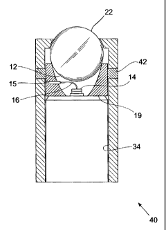
The LED 14 is combined with the ray forming contact assembly 10, LED variable
optical assembly 20 and the LED lens retaining electrical sleeve assembly 30
to form a
complete LED electro-optic assembly 40 as shown in Fig. 4. LED 14 is bonded or
soldered
to the thermal heat sink 18 made of an electrically conductive material. Once
the LED 14 is
contacted to the thermal heat sink 18 with the insulating material 19, the ray
forming contact
assembly 10 is bonded in place. Again, the top surface of the LED 14 is bonded
to the
conductive metal pin 15 via the gold wire 16. The pin 15 is preferably coated
with gold and
is pressed into the metal contact assembly. Because the contact assembly metal
is selected
for reflectivity and electrical conductivity, it will direct the LED output
and serve to
electrically connect the top surface of the LED 14 to the outside surface of
the ray forming
contact assembly 10. Next, the LED variable optical assembly 20 is installed
preferably with
a ball optic lens 22a.
Finally, the LED lens retaining electrical sleeve assembly 30 is installed
while
applying the structural adhesive 34 on the thermal heat sink 18. The reflector
12 is
preferably bonded to the thermal heat sink 18 with the structural adhesive 34.
So, the
structural adhesive 34 functions to hold the assembly securely together,
providing some
thermal conduction and additional electrical insulation from the thermal heat
sink 18.
8
CA 02589570 2009-06-03
WO 2006/001928 PCT/US2005/016900
Additionally, a conductive adhesive 42 is preferably applied to the slots 36
to bond the
outside sleeve 32 to the reflector 12. Alternatively, as discussed above, a
wire, preferably
aluminum (not shown) may be used to wire bond between the reflector 12 inside
the
assembly and the outside sleeve 32 preferably made of aluminum. Preferably,
inultiple wire
bonds are used to bond the reflector 12 and a recess (not shown) below the
surface of the
outside sleeve 32. Also, the recess is desirably coated for protection. The
conductive
material is heat cured and the complete LED electro-optic assembly 40 is
formed. Again, the
assembly 40 shows only a single LED 14, multiple LED devices may preferably be
bonded to
the assembly.
Individual alignment of the LED 14 or multiple LEDs is required because no two
individual LED assemblies are exactly the same. Differences arise from the
positioning of
the chip 14 inside the reflector 12, the positioning of the reflector cup 12,
the positioning of
the electrodes l0a and lOb, and the positioning of the optic lens 22. All of
these factors
affect the geometry and direction of the beam of light. Due to the
manufacturing process of
individual LED assemblies, the components in individual LED assemblies exhibit
a very
wide range of positional relationships. Therefore, for any application that
requires
illunzination of a specific area, each individual LED assembly must be
manually aligned and
then permanently held in place by some means of mechanical support.
While a single LED is used herein to illustrate the invention, it will be
understood by
those skilled in the art that the invention described herein applies to a
plurality of LEDs or
LED array. A plurality of LEDs may be arranged in any manner as desired for
illumination.
Even though, in the present invention the LED 14 is shown to be a rectangular
frame,
those of ordinary skill in the art will understand that according to the
disclosed invention,
LED iliuminators may be formed in any shape suitable to provide light for a
wide array of
applications, including but not limited to photocuring, video, shop windows,
photography or
9
CA 02589570 2006-12-12
WO 2006/001928 PCT/US2005/016900
specialty product displays. Because of the durability and rugged construction
of the disclosed
LED illuminator, it may be used in outdoor settings, marine applications, or
hostile
environments.