Note: Descriptions are shown in the official language in which they were submitted.
CA 02589822 2007-05-30
WO 2006/065934 PCT/US2005/045309
STACK-UP CONFIGURATION FOR A WIRELESS COMMUNICATION DEVICE
RELATED APPLICATION
The present application relates to co-pending United States Application No.
11/014,541 entitled STACK-UP CONFIGURATION FOR A WIRELESS
COMMUNICATION DEVICE, of concurrent ownership, which is incorporated herein by
reference in its entirety.
FIELD OF THE INVENTION
This invention relates generally to a component configuration in a wireless
communication device, and more specifically to a component stack-up
configuration of a
wireless communication device to reduce a Specific Absorption Rate (SAR)
level.
BACKGROUND
As the wireless communication industry continues to grow, the demand increases
for smaller and smaller wireless communication devices. A wireless
communication
device also may be referred to herein as a "wireless device," a "handset," a
"cellular
phone", a "mobile phone", etc. Decreasing the size of a wireless device
presents design
challenges including the challenge of placing device components within a
smaller
volume. Additional challenges include maintaining acceptable levels of radio
frequency
(RF) energy radiated from the wireless device in a concerned near-field range
while
maintaining radiated efficiency of the device.
When the RF module is transmitting, a power amplifier magnifies an electronic
signal and then broadcasts this modulated energy into the air through the
antenna. A first
portion of this energy travels through free space to the target destination.
Another portion
of this energy is dissipated as heat within the device. Finally, some of the
energy is
absorbed by objects near the device, including the user's body.
The power density surrounding an antenna of a wireless device varies as a
function of, for example, distance from the antenna and orientation of the
antenna. The
fields around an antenna typically are divided into two regions. A first
region is one near
the antenna called the near field, and a second region is one at a large
distance from the
antenna called the far field. The boundary between the two is often taken to
be at the
CA 02589822 2007-05-30
WO 2006/065934 PCT/US2005/045309
2
radius, R, where R = 2L2/A, where L is the maximum dimension of the antenna
and A is
the wavelength. The far field is the region where the radiation pattern is
independent of
distance from, e.g., a transmitting antenna. The near field is the region that
is closest to
the transmitting antenna and in which the field pattern depends on the
distance from the
antenna.
Limits for safe human exposure to radio frequency (RF) energy radiated from a
wireless device in the near field are given in terms of a unit referred to as
the Specific
Absorption Rate (SAR). Specific Absorption Rate is an amount of radio
frequency energy
absorbed by the body when using a radio transmitter. The acceptable SAR level
varies
from country to country. The U.S. Federal Communications Commission (FCC)
limits the
amount of acceptable exposure to RF energy from a mobile phone to a specific
local (or
spatial peak) SAR level of 1.6 watts per kilogram of tissue (1.6 W/kg). When
the wireless
device is operating within these limits, the device poses no hazards to users.
Thus,
compliance with applicable near-field exposure limits must be considered in
any mobile
phone design.
The SAR levels of various phones vary due in part to the fact that SAR is a
function of many different parameters, including device geometry, transmission
frequency, amplifier power level, antenna location, etc. A typical stack-up
configuration
of a prior art cellular phone 70 is shown in Figure 4. The phone 70 is encased
in a
housing 88 having a front face 84 and a back face 86. Components of the phone
70
include a circuit board 74 that holds processing circuitry (not shown) for
controlling a
display 72, a key pad 80, RF and other noisy, i.e., radiating, components 90
enclosed by
canister-type shielding 76, and other device components (not shown). An
antenna 82 is
coupled through a feed point 92 to a transmitter and receiver on the circuit
board 74. A
battery 78 also is encased within the housing 88 for powering the components
of the
device 70.
Continuing with Figure 4, the prior art stack-up configuration for the phone
70 is a
display 72 on the front face 84 of the housing 88, which is stacked above the
circuit board
74, which may have one or more canister-type shields 76 above and below the
circuit
board for shielding noisy components. The battery 78 is stacked below the
circuit board,
and typically is accessible through a battery door 94 on the back surface 86
of the
CA 02589822 2007-05-30
WO 2006/065934 PCT/US2005/045309
3
housing 88. In addition to the canister-type shields 76 covering the noisy
components
residing on the circuit board, the phone 70 of the prior art requires
additional shielding
(not shown), referred to herein as compliance shielding, to bring the phone 70
into SAR
compliance since high energy density appears immediately above the front face
84. This
additional shielding may include foil, RF absorbing material, metalized
plastic, and metal
brackets, etc.
The shielding within the phone 70 that is used to comply with acceptable SAR
levels continues to present a significant burden in the manufacture of the
phone in terms
of actual design efforts, iteration of compliance testing, and costs for the
additional
compliance shielding. The above described challenges are amplified as phone
sizes
decrease. Thus, it is desirable to continue innovations in the industry that
lower the SAR
level of the phone before the addition of the compliance shielding, and that
reduce final
costs of the phone in design and material costs.
SUMMARY
A wireless communication device includes a housing with a back face and a
front
face for holding a display and keypad. A battery for providing power to the
components
of the wireless communication device sits within the housing and at least
partially
between the display and a front surface of a circuit board. The circuit board
holds
processing and RF circuitry for the wireless communication device. The back
surface of
the circuit board holds radiating circuit components which are shielded by
canister-type
shielding. An external or internal antenna is connected to the circuit board
at a feed
point. The antenna in one embodiment of the invention is stacked below the
circuit
board, that is, between the back face of the housing and the back surface of
the circuit
board.
The placement of the battery in a space between the display and the circuit
board
decreases the Specific Absorption Rate measured at a set distance above the
front face
of the housing as compared to a traditional device stack up configuration in
which the
battery is placed below the circuit board and is accessible from a back face
of the
housing. The decrease in the SAR level decreases the amount of additional
compliance
shielding required to comply with acceptable SAR levels. This particularly
advantageous
as the size of wireless devices continue to decrease.
CA 02589822 2007-05-30
WO 2006/065934 PCT/US2005/045309
4
The stack up configuration of the battery and display above the circuit board
also
can provide a cavity having an increased volume for holding a speaker. The
volume of
the cavity is determined by the combined heights of the battery and the
display, the width
of the circuit board or housing, and the difference in the length of the
circuit board and the
battery. The increased cavity volume can improve the quality of sounds from
the speaker
of the wireless communication device.
' BRIEF DESCRIPTION OF THE DRAWINGS
The described embodiments are to be considered in all respects as illustrative
and
not restrictive. It should also be understood that the invention is not
limited to the
particular embodiments illustrated and described herein, but is capable of
many
rearrangements, modifications, and substitutions without departing from the
scope of the
invention. As such, the details of the present invention, both as to its
structure and
operation, may be gleaned in part by study of the accompanying drawings
described
below, in which like reference numerals refer to like parts.
Figure 1 is a side view of a stack-up configuration of an embodiment of the
invention, having an external antenna.
Figure 2 is an end view of a stack-up configuration of a second embodiment of
the
invention.
Figure 3 is a perspective view of a wireless device assembly of another
embodiment of the invention having an internal antenna.
Figure 4 is a side view of a stack-up configuration of the prior art.
Figure 5 is a graph of the energy density of the near field for the stack-up
configuration of the present invention as compared the near field for the
stack-up
configuration of the prior art, given a distance from the front face 84 in
Figure 4 or the
front face 6 in Figure 1.
Figure 6 illustrates radiation levels of a prior art stack-up configuration
with respect
to the surface of a user's head.
Figure 7 illustrates decreased radiation levels of an embodiment of the
present
invention with respect to the surface of a user's head.
Figure 8 is a block diagram of the wireless communication device of one
embodiment of the stack-up configuration.
CA 02589822 2007-05-30
WO 2006/065934 PCT/US2005/045309
Figure 9 is a circuit diagram of device circuitry for an embodiment of the
invention.
DETAILED DESCRIPTION
As the wireless industry expands, cell phone manufactures are developing
innovative wireless devices that are smaller and smaller in size. The
decreasing size of
5 phones exposes more radio frequency (RF) energy to the user's head, measured
by a
Specifc Absorption Rate (SAR) level, in the near field and radiates less RF
energy in the
far field. Thus, to reduce the human exposure and improve the radiated
efficiency while
maintaining a small-sized phone is very challenging. The present invention
addresses
this challenge by presenting an innovational stack-up configuration of the
components
within the phone.
As discussed above, the prior art phones as illustrated in Figure 4 have a
traditional mechanical stack-up from a top surface of a phone to a back
surface. The
traditional stack-up is a display, e.g., liquid crystal display (LCD), on the
top surface,
followed by a main board, shielding and a battery. Typically, the antenna feed
point is on
the main board. In contrast, the stack-up configuration of one embodiment is
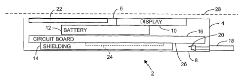
illustrated in
Figure 1. A wireless device 2 is enclosed in a housing 4 having a front face 6
and a back
face 8. The top surface 6 of the wireless device 2 holds the display 10 and
keypad 22. A
battery 12 is housed behind the display and above a circuit board 16. The
circuit board
16 holds the majority of the electronic circuitry for the wireless device 2
including noisy
components 24, that is, components that radiate RF energy. The radiating
components
24 are shielding by shielding materials 14 such as canisters, RF absorbing
material,
metalized plastic covers, etc. In the illustrated embodiment of Figure 1, the
antenna 18
is an external antenna 18 having an antenna feed point 20 on the back surface
26 of the
circuit board 16. RF energy of a modulated RF signal radiates from the antenna
18
creating the near fields and the far fields.
The mechanical stack up configuration of Figure 1 decreases the amount of
energy radiated in the concerned near field as compared to the prior art stack-
up
configuration of Figure 4. Specifically, the placement of the battery 12
between the
display 10 and the circuit board 16 contributes to the decrease in the
radiated energy in
the concerned near field area. As discussed below, simulation for energy
density
distribution in free space is performed at a plane 28 adjacent the front face
6 of the
CA 02589822 2007-05-30
WO 2006/065934 PCT/US2005/045309
6
device 2. The plane 28, which is 0.5mm above the front face, also approximates
the
placement of the user's head when using the device 2.
Figure 5 is a graph of the free space energy density (J/m3) distributed on a
plane
28 in Figure 4 for a traditional, stack-up, as shown by curve 90, and
distributed on a plane
28 in Figure 1 for an embodiment of the present invention stack-up, as shown
by curve
92. Both simulations are done without including the compliance shielding as
discussed
above. The plane 28 is 0.5mm above the front face. The sample simulation
results taken
on a'plane 28 as shown in Figures 1 and 4 are shown for illustrative purposes
only.
Other simulations may result in varying values for the energy density, and the
illustrated
example should not be considered as limiting for the embodiments of the
present
invention. The graph shows, for the concerned area, that the maximum energy
density
above the tradition stack-up of Figure 4 is approximately 3.8 times the energy
density
above the innovational stack-up configuration of Figure 1.
In one sample SAR performance simulation of the prior art stack-up
configuration
of Figure 4, with a phone thickness from the front face 84 to the back face 86
of 22 mm,
the average SAR based on IEEE standard 1529 is 2.10 W/kg at 24 dBm. This
simulation
result is taken without the compliance shielding as discussed above. Thus, for
this
particular sample prior art phone to attain the required SAR standard of 1.6
W/kg, the
device housing would have to include additional compliance shielding. In
comparison, the
innovational stack-up of Figure 1, with a same thickness of 22 mm, has an
averaged SAR
based on IEEE-1529 of 1.58 W/kg at 24 dBm. For this simulation analysis, the
SAR
value is reduced for the stack-up configuration of the present invention by
approximately
24.8%. Thus, the amount of compliance shielding required to bring the sample
present
invention phone into compliance with the SAR standard is reduced. This
reduction
represents cost savings in design time, manufacture time and materials.
Figures 6 and 7 are provided to illustrate a SAR performance as described
above,
and are based on the sample simulations. Figure 6 illustrates a user's head
102 with a
prior art phone 104 against his or her head 102. Specific Absorption Rate
power density
"bands" A, B, C, D in W/kg decrease with distance from the source 104. Band A
represents the area on the user's head absorbing the highest power density. In
comparison, the SAR power densities of an embodiment of the present invention
are
CA 02589822 2007-05-30
WO 2006/065934 PCT/US2005/045309
7
reduced as shown in Figure 7. As shown with reference to bands A', B', C', D',
the area
of the user's head 102 absorbing the highest power density is significantly
smaller than
that of the prior art.
A simulated radiated performance in free space, in a far field, for a sample
traditional stack-up has radiation efficiency of 92.84% with a directivity of
2.73 dBi, and a
gain of 2.41 dBi. In comparison, the stack-up configuration of a sample
embodiment of
the present invention yields a radiation efficiency of 92.86% with a
directivity of 2.75 dBi,
and a gain of 2.43 dBi. Thus, both the traditional stack-up and the innovated
stack-up
have the same radiated performance in free space. However, in a far field, for
a prior art
sample next to the head, the simulation results show a radiated efficiency of
22.77% with
a directivity of 5.98 dBi, and a gain of -0.45 dBi. In comparison, the stack-
up
configuration of a sample embodiment of the present invention yields a
radiation
efficiency of 32.72% with a directivity of 5.89 dBi, and a gain of 1.04 dBi.
Therefore, the
innovational stack-up configuration has a better antenna efficiency of
approximately 10%
in a far field as compared to the traditional stack-up while the sample is
held next to a
human head.
Figure 2 illustrates an end view of the device 30 of another embodiment of the
invention. The stack up configuration along a height axis, H, is the circuit
board 36
above the shielding 38 and external antenna 40, the battery 34 above the
circuit board
36, and the display 32 above the battery 34. As shown, the device 30 does not
require a
particular placement of the components with respect to a length axis L and
width axis W
of the device 30 to obtain a reduction in the SAR. In one embodiment of the
device 30 of
Figure 2, the battery 34 is accessible through a battery door 44 in the
housing 42.
Figure 3 is a perspective view of another embodiment of the wireless device
stack-
up configuration 50 having an internal antenna 66 connected to the circuit
board 54 by a
feed point 68. The battery 58 is stacked below the display 52 and keypad (not
shown),
and above the circuit board 54. Radiators and other components such as memory
on the
bottom surface of the circuit board 54 are shielded by shields 56. In this
embodiment, the
speaker 60 is placed in the volume 64 left open from the stack-up of the
battery 58 and
the display 52. This volume 64 improves the sound quality of the speaker 60.
Also
shown in this space 64 is the microphone 62.
CA 02589822 2007-05-30
WO 2006/065934 PCT/US2005/045309
8
Figure 8 is a block diagram 110 of the components of an embodiment of the
present invention showing a relative position with respect to a housing front
and back
surfaces. The display 124 and keypad 126 on a front face of the device 110 are
controlled by device circuitry on the circuit board 120. A speaker 128 and
microphone
130 send and receive audio signals to the device circuitry 120. The power
supply 122,
e.g., a battery, supplies the components of the device 110 with power through
the circuit
board 120. An antenna 116 is connected by a feed point 118 to the circuit
board 120.
Shielding 132 cover at least some of the circuitry on the circuit board 120.
Figure 9 is a block diagram illustrating a wireless communication device 150
that
may be used in connection with the various embodiments described herein.
However,
other wireless communication devices and/or architectures may also be used, as
will be
clear to those skilled in the art. In the illustrated embodiment, wireless
communication
device 150 comprises an antenna 152, a multiplexor 154, a low noise amplifier
("LNA")
156, a power amplifier ("PA") 158, a modulation circuit 160, a baseband
processor 162, a
speaker 164, a microphone 166, a central processing unit ("CPU") 168, a data
storage
area 170, and a user interface 172. In the wireless device 150, radio
frequency ("RF")
signals are transmitted and received by antenna 152. Multiplexor 154 acts as a
switch,
coupling antenna 152 between the transmit and receive signal paths. In the
receive path,
received RF signals are coupled from a multiplexor 154 to LNA 156. LNA 156
amplifies
the received RF signal and couples the amplified signal to a demodulation
portion of the
modulation circuit 160. The demodulator strips away the RF carrier signal
leaving a
base-band receive audio signal, which is sent from the demodulator output to
the base-
band processor 162. If the base-band receive audio signal contains audio
information,
then baseband processor 162 decodes the signal, converts it to an analog
signal, and
sends it to the speaker 164.
The baseband processor 162 also receives analog audio signals from the
microphone 166. These analog audio signals are converted to digital signals
and
encoded by the base-band processor 162. The base-band processor 162 also codes
the
digital signals for transmission and generates a base-band transmit audio
signal that is
routed to the modulator portion of modulation circuit 160. The modulator mixes
the base-
band transmit audio signal with an RF carrier signal generating an RF transmit
signal that
CA 02589822 2007-05-30
WO 2006/065934 PCT/US2005/045309
9
is routed to the power amplifier 158. The power amplifier 158 amplifies the RF
transmit
signal and routes it to the multiplexor 154 where the signal is switched to
the antenna
port for transmission by antenna 152. The baseband processor 162 is also
communicatively coupled with the central processing unit 168 which has access
to a data
storage area 170. The central processing unit 168 is configured to execute
instructions
(i.e., computer programs or software) that can be stored in the data storage
area 170.
Computer programs can also be received from the baseband processor 162 and
stored
in the data storage area 170 or executed upon receipt.
The description and drawings contained herein are particular embodiments of
the
invention and are representative of the subject matter broadly contemplated by
the
invention. However, the invention encompasses other embodiments that will be
obvious
to those skilled in the art. Accordingly, the scope of the invention is
limited only by the
appended claims.
WE CLAIM: