Note: Descriptions are shown in the official language in which they were submitted.
CA 02590086 2007-06-11
WO 2007/001985 PCT/US2006/023815
PROJECTILE FOR AN ELECTRICAL DISCHARGE WEAPON
FIELD OF THE INVENTION
The present invention relates generally to the field of an electrical
discharge weapon
for immobilizing a live target. More specifically, the present invention is
related to an
electrical discharge weapon having an improved shoclc circuit and a method for
operating the
same.
BACKGROUND OF THE INVENTION
Electrical discharge weapons are weapons that connect a shocking power to a
remote
live target by meaiis of darts and/or trailing wires fired from the electrical
discharge weapons.
The shocks debilitate violent suspects, so peace officers can more easily
subdue and capture
them. Stun guns, by contrast, connect the shocking power to the live target
that are brought
into direct contact with the stun guns to subdue the target. Electrical
discharge weapons and
guns are far less lethal than other more conventional fireanns.
In general, the basic idea of the above described electrical discharge weapon
s is to
disrupt the electric communication system of muscle cells in a live target.
That is, an
electrical discharge weapon generates a high-voltage, low-ainperage electrical
cliarge. When
the charge passes into the live target's body, it is combined with the
electrical signals from the
brain of the live target. The brain's original signals are mixed in with
random noise, making
it very difficult for the muscle cells to decipher the original signals. As
such, the live target is
stunned or temporarily paralyzed. The current of the charge may be generated
with a pulse
frequency that mimics a live target's own electrical signal to further stun or
paralyze the live
target.
To dump this high-voltage, low-amperage electrical charge, the electrical
discharge
weapon includes a shock circuit having multiple transfonners and/or
autoformers that boost
the voltage in the circuit and/or reduce the amperage. The shock circuit may
also include an
oscillator to produce a specific pulse pattern of electricity and/or
frequency. In one
einbodiment, the charge is then released to the live target via a charge
electrode and a ground
electrode respectively positioned on a charge dart and a ground dart that are
both connected
to the weapon by long conductive wires. In the embodiment, the long conductive
wires are
considered necessary to maintain low force factors necessary for a weapon
delivery system
which is presumed incapable of seriously injuring a human target, but which is
also capable
of propelling a projectile at a target for a practical range. That is, it is
desirable to use a small
propellant charge and a light weight projectile.
However, a disadvantage to such a design of using two wired darts is that both
minimum and maximum range are sacrificed. That is, as known to those skilled
in the art,
CA 02590086 2007-06-11
WO 2007/001985 PCT/US2006/023815
depending on the angle between the weapon's bores, the charge and ground darts
will not
spread enough at closer ranges to insure an adequately large current path
through the target,
unless the marksman is luclcy enough to impact a particularly sensitive area
of the body. At
further ranges the darts will have spread too far apart for both of them to
impact the target as
needed to complete the current path through the target. In addition, the wired
darts could ilot
pass down the bore of most conventional firearms.
Moreover, if the wires are not deployed to their maximum range and length,
they will
hang from the cartridge over the bottom of the port or firing bay and
frequently rest laxly on
the ground in close proximity to each other or even resting upon or
overlapping each other for
portions of their lengths. Accordingly, the wires have to be insulated by
heavy insulation to
prevent them from being shorted with each other. The weight of the insulation
further limits
the range of the darts and the type of firearins that can project these darts.
In view of the foregoing, it would be highly desirable to create a weapon for
immobilization and capture of a live target having projectiles or missiles
that do not require
trailing wires comlected to the weapon while still allowing the projectiles or
missiles to
maintain a low less lethal force factor (i.e., being light in weight and
capable of being
propelled using a small propellant change) and to provide a sufficient stun
(shock) power.
Also, it would be desirable to provide a light weight shock circuit for such a
weapon that
shocks with sufficient power to disable, but that can be entirely located in
the less lethal
projectile itself.
SUMMARY OF THE INVENTION
The present invention relates to a system and/or an associated method for
providing
an electrical discharge weapon and/or a method for using the same that
includes a shock
circuit having a low power consumption, a high power efficiency, and/or a low
weight. In
one embodiment, the electrical discharge weapon includes a high efficiency
circuit that
would reduce the weights of shock circuits while providing a more effective
and safer power
level, so that the circuits may be entirely contained in a projectile of the
weapon and the need
for range limiting trailing wires can be eliminated.
In one embodiment of the present invention, a wireless projectile projected
from an
electrical discharge weapon for immobilizing a live target is provided. The
wireless
projection includes a projectile shell and a shock circuit. The shock circuit
is integrated
within the projectile shell and includes a battery source, an inverter
transformer, an
independent oscillator, and a switch. The inverter transformer has a primary
coil of the
inverter transforiner and a secondary coil of the inverter transformer. The
switch is
connected between the inverter transformer and a common voltage node ( or a
ground) and is
also connected to the independent oscillator. In the shock circuit, the
independent oscillator
triggers and re-triggers the switch to supply an energy pulse from the battery
source to the
2
CA 02590086 2007-06-11
WO 2007/001985 PCT/US2006/023815
primary coil of the inverter transformer for a predetermined time period.
In one embodiment of the present invention, a method to immobilize a live
target
through electricity is provided. The method includes: oscillating an
independently controlled
waveform from a positive voltage to a ground voltage; driving a transistor via
the
independently controlled waveform to turn ON and OFF; energizing and de-
energizing an
energy from a battery source tllrough a primary coil of an inverter
transformer via the
transistor driven by the independently controlled waveform; coupling the
energized and de-
energized energy from the primary coil of the inverter transfonner to a
secondary coil of the
inverter transfonner; stepping up a voltage of the energized and de-energized
energy,from the
secondary coil of the inverter transformer to immobilize the live target; and
providing the
stepped-up energy to the live target to immobilize the live target. In the
present method, the
energy provided to the live target is not greater than nine watts.
A more complete understanding of the electrical discharge weapon will be
afforded to
those skilled in the art and by a consideration of the following detailed
description.
Reference will be made to the appended sheets of drawings which will first be
described
briefly.
BRIEF DESCRIPTION OF THE DRAWINGS
These and other features and aspects of the present in.vention will be more
fully
understood when considered with respect to the following detailed description,
appended
claims, and accompanying drawings.
FIG. 1 illustrates an exemplary electrical discharge weapon.
FIG. 2 illustrates a driving waveform of a relaxation oscillator.
FIG. 3 illustrates a shock circuit using a relaxation oscillator.
FIG. 4 illustrates a waveform passing through a Mylar gap.
FIG. 5 illustrates an output waveform of a shock circuit using a relaxation
oscillator.
FIG. 6 illustrates an shock circuit using an independently driven oscillator.
FIG. 7 illustrates a resonate waveform of the shock circuit of FIG. 6.
FIG. 8 illustrates an output waveform of the shoclc circuit of FIG. 6
FIG. 9 illustrates another shock circuit using an independently driven
oscillator.
FIG. 10 illustrates yet another shock circuit using an independently driven
oscillator.
FIG. 11 illustrates an electrical discharge weapon system projecting a
wireless
projectile.
FIG. 12 illustrates a top view of the projectile of FIG. 11
FIG. 13 illustrates a bottom view of the projectile of FIG. 11
FIG. 14 illustrates a cutaway side view of the projectile of FIG. 11
FIG. 15 illustrates a cross-sectional view of a secondary propulsion device of
the
projectile of FIG. 11.
3
CA 02590086 2007-06-11
WO 2007/001985 PCT/US2006/023815
FIGs. 16 and 17 illustrate in sequence a terminal operation of the projectile
of FIG.
11.
DETAILED DESCRIPTION OF THE INVENTION
In the following detailed description, only certain exemplary embodiments of
the
present invention are sllown and described, by way of illustration. As those
skilled in the art
would recognize, the described exemplary einbodiments may be modified in
various ways, all
without departing from the spirit or scope of the present invention.
Accordingly, the
drawings and description are to be regarded as illustrative in nature, and not
restrictive.
There may be parts shown in the drawings, or parts not shown in the drawings,
that
are not discussed in the specification as they are not essential to a complete
understanding of
the invention. Like reference numerals designate like elements.
Referring to Fig. 1, an example of an electrical discharge weapon is shown
which
includes a housing 1, a shock circuit 10, a trigger 20, battery or batteries
30, a first
electrically conductive dart 50, and a second electrically conductive dart 60.
Each of the
darts 50, 60 is coimected to the housing by elongate first and second
electrically conductive
wires 16, 17. The wires 16, 17 are coiled in the housing 1 and unwind and
straighten as the
darts 50, 60 travel througll the air toward a target. The length of wires 16,
17 can vary but the
increasing distance of the spread between them limits raiige (typically about
six to nine
meters or twenty to thirty feet)
In operation, an electrical charge which travel into the wire 16 and the dart
50 is
activated by squeezing the trigger 20. The power for the electrical charge is
provided by the
battery 30. That is, when the trigger 20 is turned on, it allows the power to
travel to the shock
circuit 10. The shock circuit 10 includes a first transformer that receives
electricity fioin the
battery 30 and causes a predetermined amount of voltage to be transmitted to
and stored in a
storage capacitor (e.g., a Mylar cap). Once the storage capacitor stores the
predetermined
amount of voltage, it is able to discharge an electrical pulse into a second
transformer and/or
autoformer. The output from second transformer then goes into the first wire
16 and the dart
50. The darts 50, 60 are also projected through the air to the target by the
squeeze of the
trigger 20. When the darts 50, 60 contact the target, charges from the dart 50
travel into tissue
in the target's body, then through the tissue into the second dart 60 and the
second conducting
wire 17, and then to a ground in the housing 1. Pulses are delivered from the
dart 50 into
target's tissue for a predetermined amount of seconds. The pulses cause
contraction of
skeletal muscles and make the muscles inoperable, thereby preventing use of
the muscles in
locomotion of the target.
Typically, the shocks from an electrical discharge weapon are generated by a
classic
relaxation oscillator that produces distorted saw tooth pulses as is shown in
FIG. 2. A shock
circuit having a relaxation oscillator is shown as FIG. 3.
4
CA 02590086 2007-06-11
WO 2007/001985 PCT/US2006/023815
Referring to FIG. 3, power is supplied to the shock circuit from a battery
source 160.
The closure of a switch SWl (e.g., the trigger 20 of FIG. 1) connects the
battery source 160
with an inverter transformer TI. In FIG. 3, a tickler coil 110 of the inverter
transformer T1
between PAD1 and PAD2 is used to form the classic relaxation oscillator. A
primary coil
100 of the inverter transfonner Tl is connected between PAD3 and PAD4. Upon
closure of
the power switch SW1, the primary coil 100 of the inverter transformer Tl is
energized as a
current flows through the coil 100 from PAD3 to PAD4 as the power transistor
Q1 is turned
ON. The ticlcler coil 110 of the inverter transformer T1 is energized upon
closure of the
power switch SWI through a resistor R8 and a diode D3. The current through the
tickler coil
110 also forins the base current of the power transistor Q1, tllus causing it
to turn ON. Since
the tickler coil 110 and the primary coil 100 of the inverter transfonner T1
oppose one
another, the current through power transistor Q1 causes a flux in the inverter
transformer T1
to, in effect, backdrive the tickler coil 110 and cut off the power transistor
Q1 base current,
thus causing it to turn OFF and forming the relaxation oscillator.
In addition, a secondary coil 120 of the inverter transformer Tl between PAD5
and
PAD6 is connected to a pair of diodes D4 and D5 that forms a half-wave
rectifier. The pair
of diodes D4 and D5 are then serially connected with a Mylar cap 130 and then
with a
primary coil 140 of the output transformer T2. The primary coil 140 of the
output
transformer T2 is connected between PAD7 and PAD 8. The Mylar cap 130 is
selected to
have particular ionization characteristics tailored to a specific spark gap
breakover voltage to
"ttule" the output of the shock circuit.
In operation and as described above, the classic relaxation oscillator
produces
distorted saw tooth pulses as is shown in FIG. 2. The distorted saw tooth
pulses generated by
the relaxation oscillator charge the Mylar cap 130, which can be a 0.22 to
0.94 mfd Mylar foil
capacitor.
Referring also to a waveform 130' of FIG. 4, when sufficient energy is charged
on the
Mylar cap 130 as schematically represented by the rising part 130a' of the
waveform 130', a
gas gap brealcs down as schematically represented by the falling part 130b' of
the waveform
130'. This energy is then passes through the primary coil 140 of output or
step up
transfonner T2, which typically has a turn ratio of 1:35 to 1:37 primary coil
140 to secondary
coil 150. A train of trailing sinusoidal waves are then output by secondary
coil 150 of the
output transformer T2 as is shown in FIG. 5. This output current of FIG. 5 is
essentially a
dampened and inverted saw tooth pulse. Its trailing alternating features are
the result of
"ringing" or tuning in the inverter transformer T1 (the primary or secondary
coils 100, 120
inducing steadily declining currents and fields back and forth in each other
as the interacting
coils magnetic fields repeatedly collapse, regenerate and collapse again). The
bulk of the
shock energy appears in the first half cycle of the pulses. Though significant
energy does
appear in the total train of waves trailing thereafter, this tuned energy of
the second half cycle
CA 02590086 2007-06-11
WO 2007/001985 PCT/US2006/023815
is in large measure wasted, as most of the trailing pulses are of insufficient
amplitude to
cause a debilitating shock.
In addition, since the self actualizing relaxation oscillator includes a
bipolar transistor
Ql, switching losses may occur. That is, the oscillator fly back or tickler
coil 110 is slow to
reverse bias the transistor QI because of its magnetic feedback. This slow
ramping or rise
time limits how fast the transistor Ql can switcli without burning up. The
slow switching
causes power losses. Moreover, because of the slow switching speed, the shock
circuit
requires larger and bullcier transformers T1, T2, as transformer size is
directly proportional to
switching speed. As such, the shock circuit of FIG. 3 typically operates at
less than 20%
efficiency.
In an einbodiment of the present invention and referring to FIG. 6, a shoclc
circuit 200
includes an independent, non-self actualizing and/or driven oscillator 210 and
a tank circuit
220 that allows the shock circuit 200 to operate with much higher efficiency.
In the shock circuit 200 of FIG. 6, a power is supplied from a battery source
230 to an
inverter transformer TI'. In FIG. 6, a primary coil 240 of the inverter
transformer Tl' is
connected between PAD 10 and PADI1. In the embodiment, an oscillating
capacitor C is also
shown to be comlected between PAD 10 and PAD 11 and in parallel with the
primary coil
240. As such, the tank circuit 220 of an exemplary embodiment of the present
invention is
formed by the primary coi1240 of the inverter transformer T1' and the
oscillating capacitor C.
A power switch 250 is connected between the inverter transformer T1' and a
ground. The
power switch 250 (or a base or a gate of the power switch 250) is also
connected to the
independent oscillator 210.
In more detail, the primary coil 240 of the inverter transformer Tl' is
energized as
current flows through the coil 240 from PAD 10 to PAD11 as the switch (or
transistor) 250 is
turned ON. The independent oscillator 210 is coupled to the switch 250 (e.g.,
at the base or
the gate of the switch 250) to turn the switch 250 ON and OFF. A secondary
coil 260 of the
inverter transformer Tl' between PAD 12 and PAD 13 is connected to a full-wave
rectifier
270. The full-wave rectifier 270 is then serially connected with a Mylar cap
280 and then
with a primary coil 290 of the output transformer T2'. The primary coil 290 of
the output
transformer T2' is connected between PAD14 and PAD 15.
In operation, the capacitor C and the primary coil 240 of the embodiment of
FIG. 6
form a second energy saving oscillator. That is, the capacitor C stores energy
in the form of
an electrostatic field, while the priinary coil 240 uses a magnetic field to
store energy. As
such, any unused energy of the primary coi1240 charges up the capacitor C. The
capacitor C
then discharges through the primary coil 240. As the capacitor C discharges,
the primary coil
240 creates a magnetic field. That is, as the capacitor C discharges, the
primary coil 240 will
try to keep the current in the circuit moving, so it will charge up the other
plate of the
capacitor C. Once the field of the primary coil 240 collapses, the capacitor C
has been
6
CA 02590086 2007-06-11
WO 2007/001985 PCT/US2006/023815
recharged (but with the opposite polarity), so it discharges again through the
primary coil
240.
This oscillation will continue until the circuit runs out of energy and will
oscillate at
an predetermined amplitude and frequency that depends on the size of the
primary coil 240
and the capacitor C. As such, the capacitor C can turn the significant energy
in the second
half of the total train of waves of FIG. 5 that would otherwise be wasted
(because of the
insufficient amplitude) into additional waves having the sufficient amplitude
to cause f-urther
debilitating shock. Thus, the efficiency of the shock circuit 200 is enhanced
by the capacitor
240 that is in parallel with the primary coil 240 of the transformer T1'
thereby forming the
tanlc circuit 220.
In more detail, when the tank circuit 220 is triggered by 250, it begins to
resonate.
The resonation would thereafter trail off as is shown in FIG. 7. However,
switch 240
retriggers the resonant circuit after each full cycle. Accordingly, cycles are
continuously
produced having a first half cycle and a second half cycle which is near the
same in
ainplitude as the first half cycle, as illustrated in FIG. 8. As such, the
energy from the
collapsing field of the transformer primary coil 240 is no longer wasted as is
in the circuit of
FIG. 3, if the full wave rectifier 270 is positioned between the secondary
coil 260 of the
transformer T1' and the charging Mylar cap 280.
Referring to FIG. 9, a shock circuit 200' of a more specific einbodiment of
the present
invention includes an oscillator 210' and a tank circuit 220'. In this shock
circuit 200', a
power is supplied from a battery source 230' (e.g., a 12V battery) to an
inverter transfonner
TI". The tank circuit 220' in this embodiment is formed by a primary coil 240'
of the inverter
transformer T1" and an oscillating capacitor C15. An NPN transistor 250' is
connected
between the inverter transformer T1" and a ground. A base of the NPN
transistor 250' is
connected to the oscillator 210'. A secondary coil 260' of the inverter
transformer Tl" is
connected to a first pair of diodes D4 and D2 and a second pair of diodes Dl
and W. The
first and second pairs of diodes D1, D2, D3, and D4 form a full-wave rectifier
270'. The full-
wave rectifier 270' is then serially connected with a Mylar cap 280' and then
an output
transformer T2".
In operation, the oscillator 210' creates a periodic output that varies from a
positive
voltage (V+) to a ground voltage. This periodic waveform creates the drive
function for the
PNP transistor 290'. The output voltage of the oscillator 210' is not a square
wave but a pulse
waveform that is low for about one third of its period. Wlien the oscillator
210 switches low,
it causes zener diode D27 to conduct, and in turn, causes the transistor 290'
to saturate. The
zener diode D27 is needed because the voltage Vcc, that powers the transistor
290' and the
positive voltage (V+) that powers the oscillator 210' are at different
potentials. When 290'
turns on, it in turn causes the transistor 250' to saturate. This, in turn
causes current to flow
through the primary coil 240' of the transformer Tl". This current flow causes
current to
7
CA 02590086 2007-06-11
WO 2007/001985 PCT/US2006/023815
flow in the secondary coil 260' of the transformer Ti" based on the turn ratio
of the
transformer T1". In this particular situation, the transfornler T1" has a turn
ratio of about
110:1 (or 110 to 1). A power current from the battery source 230' then flows
in the primary
coil 240' of the transformer T1" only when the transistor 250" is turned on
and is in the
process of conducting. Residual current, however, can also be flown through
the primary coil
240' as the magnetic field, initially generated by the current flow from the
battery source 230',
collapses and the tanlc circuit 220' mechanized with the primary coil 240' of
the transformer
T1" and capacitor C15 begins to resonate. This "resonant current" is also
coupled through the
transformer T1" from the primary coil 240' to the secondary coil 260' and, in
turn, also is
stepped up by the tuin ratio of the transformer T1 V.
The full wave bridge rectifier 270', mechanized with the four high voltage
diodes Dl,
D2, D3, and D4, therefore rectifies the initial voltage and current from the
power source 230'
when the transistor 250' is caused to conduct, and then the resonant voltage
and current
created as the tank circuit 220' resonates. The effect of this is to cause the
Mylar cap 280' to
charge more quickly and with more efficiency, thereby requiring less energy
drawn froni the
power source 230' tlian if the tank circuit 220' was not present in the
design.
An additional feature of this shock circuit 200' is that the transistor 250'
is a high
voltage transistor with a Vcc of greater then 1000 volts. This eliininates the
need for a
"snubber" diode across the transformer primary. A diode D6 is required,
however, because as
the tank circuit 220' resonates, it would have the capability to break down
the transistor 250'
over in the reverse direction thereby potentially damaging the transistor 250'
and "snubbing"
the tank circuit 220' resonance prematurely.
In a generalized exemplary embodiment of the present invention, a portion of a
shock
circuit that is employed to generate a high voltage used to deliver a current
pulse to an output
transformer utilizes a resonant tank circuit. The tank circuit assists in the
creation of the high
voltage level necessary to charge the Mylar cap through the fact that it
resonates at a
frequency determined by the inductance of the primary coil of an inverter
transformer and the
capacitor that is placed in parallel with it. However, the present invention
is not limited to
the above described exemplary embodiment. For example, referring to FIG. 10,
an
embodiment of a shock circuit 350 can include a digital oscillator 300 coupled
to digitally
generate switching signals to a base or a gate of a transistor 310. The
transistor 310 is
coupled in series with the primary coil 320 of a transformer 340 to
alternately conduct from
collector to emitter or source to drain of the transistor 310. The transformer
340 is coupled to
an voltage stepper 360 (e.g., an autoformer) to step-up the voltage of the
signal generated by
the transformer 340. In this embodiment, no third tickler coil is present as
is shown in FIG.
3. The digitally generated signal drives the switching transistor 310 and
transformer 340.
The driven transformer 340 allows for greater frequency operations control. If
a MOSFET
transistor is used as the transistor 340, there is a reduction in power loss
from the switching,
8
CA 02590086 2007-06-11
WO 2007/001985 PCT/US2006/023815
and the transistor 340 can switch at faster speeds.
In view of the foregoing, certain high efficiency circuits can be employed to
form
electrical discharge weapons with higher energy shoclcs with similar sizes to
weapons with
circuits having self actualizing relaxation oscillators. However, the
propriety of forming
weapons capable of producing such high powered shocks may be in question
because the
enhanced shocks may increase the weapons lethality, especially where circuits
operating at a
fraction of the power ranges that can be achieved by these circuits (e.g., at
power levels as
low as 1.5 watts and 0.15 joules per pulse at ten pps) were demonstrated to
completely
disable test subjects as early as 1971. In addition, some seventy deaths have
occurred
proximate to use of such weapons. As such, using these pistols at high power
ranges may run
contrary to the idea that electrical discharge weapons are intended to subdue
and capture live
targets without seriously injuring them. Therefore, a more laudable purpose
for such high
efficiency circuits would be to reduce the weights of shock circuits at the
lower and safer
power levels, so that the circuits can be entirely contained in projectiles
and to eliminate the
need for range limiting trailing wires.
Less lethal wireless projectiles could not, heretofore, be launched to
optimally desired
tactical ranges while maintaining safe force factors, because, as currently
produced by
various manufactures, the shock circuits that might be contained within the
projectile have
too great a weight.
The primary consideration when assessing the relative lethality of a non-
lethal
projectile is the kinetic energy that is transferred to the target upon
impact. The energy is
equal to one-half the mass of the projectile times the square of the velocity:
K.E.= r/2 mv2
This equation shows the strong dependence on velocity and a lesser dependence
on
the mass of the projectile. It is desirable to keep the velocity high to
deliver the maxiinum
kinetic energy, within the constraints of non-lethal impact to the body (blunt
iinpact trauma
and penetration). Higher velocities also have the desirable effect of
maximizing the accuracy
and flight stability of the projectile, for improved flight characteristics
and trajectory.
Much research has been done to characterize the blunt trauma and penetration
characteristics of non-lethal projectiles, and these results have been
correlated with specific
ranges of kinetic energy and kinetic energy per unit of impact area.
Acceptable impact
properties can usually be achieved by controlling the kinetic energy delivered
to the target,
maximizing the impact area that contacts the target, or by designing features
into the
projectile that absorb or dissipate energy upon impact.
When trying to find a compromise between the competing goals of maximum
kinetic
energy, optimum flight characteristics, and non-lethal impact properties, the
designer is
usually faced with sacrificing performance in one area to satisfy requirements
in another
when adjusting the velocity. One way to control the kinetic energy while
keeping the
9
CA 02590086 2007-06-11
WO 2007/001985 PCT/US2006/023815
velocity as high as possible for optimum flight considerations is to decrease
the mass of the
projectile. While this has a smaller effect on the lcinetic energy than the
velocity, it allows
the designer some flexibility to decrease the impact energy without affecting
performance.
In one embodiment of the present invention, a shoclc circuit includes a non-
self
actualizing oscillator. The shock circuit can be less than or equal to forty-
five grams,
produce a shock power that is less than nine watts, and/or produce each pulse
at an energy
range that is less than 0.9 joules. In one embodiment, each pulse is produced
at an energy
range that is not less than 0.15 joules and not greater than 0.75 joules.
In more detail, the profile of pulses used in an exemplary embodiment should
be
within the following ranges. First, the energy produced by the pulses should
be in the range
of about 0.01 to 0.8 joules or about 0.5 to 0.75 joules. Second, the width of
each pulse should
be about one to nine microseconds or about seven and a half to nine
microseconds. Tlzird, the
root-mean-square (rms) current of the pulses should be in the range of about
twenty to ninety
milliamps or about sixty-five to ninety milliamps. In addition, the pulses
should be delivered
to a target having a travel spacing (or distance) within the target to induce
enough skeletal
muscles contractions such that the live target subjected to the pulses is
actually disabled.
Referring to FIG. 11, an exemplary shock circuit of the present invention is
in.tegrated
into an exemplary projectile 512 to allow the above profiled pulses to be
delivered into a
target 520 with the required travel spacing within the target 520. As is
shown, a grenade
launcher 510 (e.g., an M203, an M79, etc.) is used to propel the projectile
512 to impact the
target 520. The impact of the target 529 has caused connectors 515 and 525 to
contact and
affix to the surface of the target 520. The distance between the grenade
latulcher 510 and the
projectile 512 can vary (typically about six to fifty meters or twenty to one
hundred fifty
feet). As is shown in FIG. 11, there are no wires extending from the grenade
launcher 510 to
the projectile 512 because the shock circuit is entirely contained in the
projectile 512. In
addition, a wire tether 530 is shown to be attached to connector 525 for
providing a selected
separating distance between the two connectors 515 and 525.
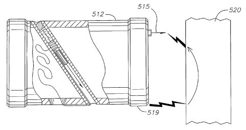
In more detail and referring to FIGS. 12-15, the projectile 512 is configured
as a
generally hollow cylinder having end caps 513 and 517, the latter having the
connector 515
extending longitudinally therefrom. A projectile of present invention,
however, is not limited
to a cylindrical shape projectile and can be any shape known to these skilled
in the art (e.g., a
sphere, a cube, etc.). As is shown, a diagonal passage 522 extends into the
projectile 512
through the center of the projectile 512 to form an opening in the radial
surface of the
projectile 512 as is sllown in FIGS. 12 and 13.
A passage 522 is covered with a Mylar tape 521 where it opens adjacent end cap
513.
The tape 521 protects a primer 528 shown in FIG. 15. As is also shown in FIG.
15, within the
passage 522 there are positioned a styrofoam 526, a foam wad 529, and a
connector body 524
terminating in the connector 525, the point of which resides near the opening
of the passage
CA 02590086 2007-06-11
WO 2007/001985 PCT/US2006/023815
522 closer to the end cap 517. A metal foil contact 519 projects from that
opening to and
over the end cap 517 terminating adjacent the front end of the projectile 512.
Also positioned
within the passage 522 are pins 532 and 534. The first pin 534 is positioned
between the
primer 528 and the styrofoam 526 and extends through the styrofoam toward the
pin 532.
The second pin 532 is connected to the wire tether 530 and which is, in turn,
connected to the
axial end of the connector body 524.
The terminal operation of the projectile 512 as it nears and engages the
target 520, is
illustrated sequentially in FIGS. 16 and 17. As shown in FIG. 16, when the
projectile 512
and the connector 515 are near the target 520 (actual distance depends upon
electrical
parameters and ambient conditions), arcing occurs through the target between
the connector
515 and the foil 519. The resulting current flow back into the projectile 512
and including
the metal wall of the passage 522, ignites the primer 528 and propels the
connector body 524
through the passage 522 and on a generally diagonal path toward the target 520
until the
connector 525 contacts and affixes to the target surface at a location spaced
from the point
that the coiuZector 515 also contacts and affixes to the target surface.
Connector 525 may be
launched from passage 522 to target 520 on or after impact with target 520 by
otlier means.
This secondary propelling of the second connector 525 only when the projectile
512 is
close to or in contact with the target 520 assures that, irrespective of the
distance to the target
520, the spacing between connectors 515 and 525 will be substantially the
same. Moreover,
the spacing will be witllin a range to virtually assure optimal disabling
effect on the target.
In one embodiment, the wire tether 530 can be about forty-six cm or eighteen
inches
long and the passage 522 can be at an angle greater than forty-five degrees,
or about seventy
degrees with respect to the axis of the projectile 512.
An embodiment of the projectile 512 can be configured as a fixed ammunition
shell
which can be fired through a conventional thirty-eight mm or forty mm bore or
which can be
between 38 to 40 mm in caliber. An einbodiment of the projectile 512 can also
be launched
by gas expansion in the launching cartridge or casing in the chamber of a
firearm. In one
embodiment, the projectile 512 should be less than 110 grains and should
produce a force of
less than about twelve newtons or ninety ft=lb/sz (pdl) on the target 520. The
shock circuit
integrated into the projectile 512 should not be greater than 45 grams or
about 25 grams and
should produce a shock power that is less than nine watts or between about two
to six watts.
Otherwise, the operation of the projectile 512 should act like a standard
shell when it is
desired to immobilize a target.
While the invention has been described in connection with certain exemplary
embodiments, it is to be understood by those skilled in the art that the
invention is not limited
to the disclosed embodiments, but, on the contrary, is intended to cover
various modifications
included within the spirit and scope of the appended claims and equivalents
thereof.
11