Note: Descriptions are shown in the official language in which they were submitted.
CA 02590150 2007-06-08
WO 2006/061780 PCT/IB2005/054081
1
Data carrier with a chip and a plurality of sensors
The invention relates to a data carrier with a chip, which stores energy as
well
as information for contact-bound or contactless inductive communication, and
with a
plurality of excitable sensors integrated in the chip, which, after
excitation, pass on a signal to
a CPU of the chip, in which the signal is processed.
The invention also relates to a method of communicating by means of chips
integrated in data carriers, in which energy as well as information from a
chip is stored for
contact-bound or contactless inductive communication, and in which a plurality
of sensors
integrated in the chip is excited, which then pass on a signal to a CPU for
the purpose of
processing.
Data carriers with a chip are widely known in the art and form part of, for
example, machine-readable travel documents (MRTD) and are usually equipped
with a chip
on a semiconductor basis which provides the possibility of both storing and
processing
complex (biometrical) information.
Data carriers with a chip are also used in value and security documents such
as
chip cards, smart cards, personal documents, passports, driving licences,
checks and
banknotes. Particularly chip cards have found their way in more and more new
fields of daily
life and have meanwhile become a natural part of modern life, with a chip
module being
integrated in the card body of the chip card. The card body may be made of
different
materials. Suitable materials are, for example, polyvinylchloride,
polycarbonate,
acrylbutadiene styrol, polyethylene terephtalate, (thermoplastic) polyurethane
(T)PU or also
paper and cardboard in which, however, also compound materials/laminates of
synthetic
material with paper, photopaper or special materials such as Tyvek of Dupont
are interesting.
The constituents of a card are referred to as card elements. Important card
elements are, for
example, foils and printing colors or inks. Card elements such as MLI
(multiple laser image),
OVI (optical variable ink), UV colors or fluorescent colors are also
important. There are
various methods of manufacturing data carriers, such as particularly the
lamination technique
and the injection molding technique. An extensive description of materials and
manufacturing methods for data carriers can be found in, for example, the book
by Y.
Haghiri/Th. Tarantino, "Vom Plastik zur Chipkarte" ("From plastic to chip
card"), Carl
CA 02590150 2007-06-08
WO 2006/061780 PCT/IB2005/054081
2
Hanser Publishers, Munich, Vienna, 1999; Chapter (2): "Kartenkorper" ("Card
bodies") and
chapter (3): "Herstellungsformen fur Kartenkorper" ("Methods of manufacturing
card
bodies").
The conventional chip modules built in the card body are substantially
independent of the type of material surrounding them. It does not "matter" to
a chip whether
it is incorporated in a PVC injection-molded card, a PC compound or a PET self-
adhesive
label. The communication or data exchange with the chip is realized either in
a contact-bound
or a contactless way (RFID technology), which are among the conventional
possibilities. In
the RFID technology, the communication is established by means of magnetic or
electromagnetic fields.
An MRTD-integrated chip module is enabled/disabled in a conventional
manner by means of a data exchange between the chip module and a testing
station, which
can also be realized in the RFID technology. In this case, the testing station
"proves" to the
chip that it possesses certain secret information. This knowledge in turn
proves to the chip
that the testing station is, for example, authorized to read the chip
contents. This process is
also referred to as conventional authentication.
Present-day chips are also equipped with a plurality of on-chip sensors. These
on-chip sensors provide the possibility of appropriate operation of the chip
by monitoring
external ambient parameters such as temperature, energy supply and incidence
of light.
Such a plurality of on-chip sensors is known from, for example, US
2002/0,186,145 Al. The known sensors are additional constituents of a chip in
a smart card
(page 2, column 1, lines 2 to 8) and are used to detect changes of a product
or its ambience
(page 1, column 2, [0013]).
Furthermore, it is known from the prior art that a plurality of on-chip
sensors
may comprise, for example, a light sensor, a temperature sensor, a frequency
sensor and a
further sensor which, when excited, pass on a signal to the CPU of the chip in
which the
signal is processed. Usually, the sensors communicate with the CPU in one of
two possible
ways. One way is to trigger an exception which is appropriately processed by
the operating
system (and, for example, repeats a computation, stops a computation or tests
computation
results in a detailed manner). Another way is to trigger a warm reset by a
sensor, i.e. the CPU
is caused to completely interrupt the program it is processing, and to repeat
it again from the
CA 02590150 2007-06-08
WO 2006/061780 PCT/IB2005/054081
3
start. This is the more drastical reaction and is usually applied for sensors
which are
considered to be critical.
The chips with a plurality of on-chip sensors known from the prior art
consequently show that sensors integrated in chips are mainly used for the
purpose of
detecting common changes of external parameters so as to communicate with the
CPU by
means of exceptions and warm resets. Consequently, the possibilities of the
chips performing
given and specific processes and operations in the CPU, which extend beyond
the
conventional possibilities based on, for example, the RFID technology and
require, for
example, specific, complex optical signals, are of course limited. In
accordance with the state
of the art, the processing of conventional RFID signals together with complex
signals
resulting from specific, complex sensor excitations and leading to new and
complex
processes cannot be performed in the chip.
It is therefore an object of the invention to provide a data carrier with a
chip
and a plurality of chip sensors in which the CPU does not only process the
conventional
signals resulting from contact-bound or contactless communication but is also
activated for
given, more complex processes requiring excitation of the chip sensors.
This object is achieved by the characteristic features defined in claim 1.
The invention is based on the recognition that the CPU of the chip is not only
made suitable for reception of and activation by the conventional signals
occurring in
contact-bound or contactless inductive communication but also for the signals
supplied in a
physically independent manner by the chip sensors that are integrated in the
chip. In this way,
the conventional possibilities of communication are accompanied by a further
possibility of
communicating with the chip, which is particularly suitable for transmitting
complex signals
required for a specific excitation to the CPU. The CPU of the chip processing
the complex
signals can then activate the chip for further processes which extend beyond,
for example, the
conventional authentication. For example, the signals transmitted through the
conventional
communication modes and the signals transmitted by the chip sensors through
separate
physical connections can also be processed in a combined manner in the CPU so
as to trigger
further processes in the chip.
An advantageous embodiment of the data carrier according to the invention is
defined in claim 2 in which the plurality of chip sensors communicates with a
filter material
in which the excitation is specifically adjustable and is adaptable to the
requirements of
CA 02590150 2007-06-08
WO 2006/061780 PCT/IB2005/054081
4
processing the signal in the CPU. This ensures that given material-dependent
chemical/physical phenomena can be utilized for the specific excitation. By
using the filter
material which communicates with the chip sensors, a chemical-physical
"filtering" is created
to a certain extent which allows only given, specific excitations of the chip
sensors and thus
also ensures that the chip only functions in the "correct" material ambience.
In this way,
material properties are combined with the chip to one functional unit. A chip
functions only
in the "correct" material environment. Conversely, in such a controlled
material environment,
the hardware properties of the chips can be verified by means of a defined
hardware
signature.
Data carriers with chips are often used in, for example, chip cards, personal
documents and checks whose materials can thus be used as filter material.
Claim 3 therefore
defines that the filter material consists of card material, whereas claim 4
defines that the filter
material consists of document material.
It is advantageous that the document material is formed as a material imprint
or as an additive.
A further preferred embodiment of the invention is characterized in that the
plurality of chip sensors includes a photosensor detecting the excitation of a
pulsed laser
beam. Different optical excitation profiles are created because the photo
sensor detects the
excitation of the pulsed laser beam. Excitation profiles thus formed are
suitable for
transmitting complex information to the chip.
Advantageously, the CPU performs a combined processing operation on a
signal of the contact-bound or contactless inductive communication and the
signal supplied
by the plurality of chip sensors. In such a combined communication, a binary
code can be
divided into two information paths and composed to the actual code in the CPU.
In this way,
for example, a logic "0" can be transmitted by using the conventional
information path and
triggering a warm reset. A logic "1" is transmitted by triggering a
photosensor and thus a
warm reset whose photosensor origin is characterized in a status variable. By
repeatedly
querying the status variables, the CPU ultimately composes the information to
be transmitted
from the single pieces of information.
An advantageous embodiment of the data carrier according to the invention is
defined in claim 9 in which the plurality of chip sensors includes a
photosensor and the filter
material consists of card material which is opaque at wavelengths of less than
800 nm and
transparent at wavelengths of 800 to 1100 nm, and of a UC converter adjoining
the card
material, as well as an interference filter laminate adjoining the UC
converter, and in which a
CA 02590150 2007-06-08
WO 2006/061780 PCT/IB2005/054081
pulsed laser beam first penetrates through the card material and then
penetrates the UC
converter. In accordance with ISO 7810, conventional card materials are
transparent only in
the NIR range at wavelengths between 800 and 1100 nm so that a pulsed laser
beam in this
wavelength range can specifically excite the photosensor and produce different
optical
5 excitation profiles, with the result that the correspondingly programmed CPU
processes
complex signals which, together with the "customary" RFID signal, activate the
chip for
further processes.
A useful variant of the data carrier according to the invention is defined in
claim 10 in which the plurality of chip sensors includes a photosensor and the
filter material
consists of the card material and a matrix adjoining the card material, which
matrix generates
modulated luminescences, and in which a pulsed laser beam first penetrates
through the card
material and then penetrates the matrix. Such a specific, pulsed excitation
triggers routines
which are distinguished from the conventional exception routines and lead to
complex
operations in the CPU.
Alternatively, the plurality of chip sensors includes at least two identical
or
different photosensors whose filter material is different, in which the filter
material consists
of the card material, and in which a pulsed laser beam penetrates through the
filter material
and excites the photosensors which separately pass on a signal to the CPU.
This has the
advantage that the information can be divided into different optical
wavelengths. This may be
used, for example, for implementing a ternary logic.
A practicable variant of the data carrier according to the invention is
defined in
claim 12 in which the plurality of chip sensors includes a photosensor and the
filter material
consists of a light converter which shifts wavelengths, and of card material
adjoining the light
converter, which card material is transparent in a wavelength range between
800 and 1100
nm, and in which a pulsed laser beam penetrates the light converter only. Such
a filter
material has the advantage that it consists of only two layers, namely of the
light converter
and the card material and can nevertheless generate complex optical excitation
profiles.
The data carrier according to the invention is advantageously integrated in a
value or security document. This takes the fact into account that data
carriers are often used
in value and security documents.
Moreover, the data carrier according to the invention can be used in a method
of communicating with chips integrated in data carriers as defined in claim
14, in which
energy as well as information from a chip is stored for contact-bound or
contactless inductive
communication and, independently thereof, a plurality of chip sensors
integrated in the chip
CA 02590150 2007-06-08
WO 2006/061780 PCT/IB2005/054081
6
is excited, which then pass on a signal to a CPU for the purpose of
processing, the excitation
being specifically adjusted by the chip for the purpose of additional storage
of information
and being adapted to the requirements of processing in the CPU.
As defined in claims 15 and 16, the chip sensors can be caused to
communicate with a filter material in which the excitation is specifically
adjusted and
adapted to the requirements of processing the signal in the CPU, while a
photosensor
detecting the excitation of a pulsed laser beam is integrated in the plurality
of chip sensors.
These and other aspects of the invention are apparent from and will be
elucidated with reference to the embodiments described hereinafter.
In the drawings:
Fig. 1 shows diagrammatically a plurality of conventional chip sensors;
Fig. 2 shows diagrammatically a card according to the invention with a chip
and a plurality of chip sensors;
Fig. 3 shows diagrammatically the plurality of chip sensors according to the
invention with a filter material provided with a matrix;
Fig. 4 shows diagrammatically the plurality of chip sensors according to the
invention with a filter material provided with a UC converter and an
interference filter laminate;
Fig. 5 shows diagrammatically the plurality of chip sensors according to the
invention with a filter material provided with a light converter;
Fig. 6 shows diagrammatically the plurality of chip sensors according to the
invention, with two photosensors.
Fig. 1 shows a plurality of conventional chip sensors 11. The chip sensors 11
provide the possibility of appropriate operation of the chip 10 by monitoring
external ambient
parameters such as, for example, temperature, power supply voltage, clock
frequency and
light incidence. The plurality of chip sensors 11 comprises a light sensor 14,
a temperature
sensor 15, a frequency sensor 16 and a further sensor 17. In the case of
excitation 12 of the
chip sensors 11, the chip sensors 11 pass on a signa118 to the CPU 19 of the
chip 10 in which
the signal 18 is processed. There are essentially two methods of processing
such a signal 18.
In one method, the CPU 19 generates an "exception" signal which is further
processed by the
CA 02590150 2007-06-08
WO 2006/061780 PCT/IB2005/054081
7
operating system of the chip 10. After introduction into an inductive
electromagnetic field 30,
the operating system of the chip 10 expects a well-defined sequence, triggered
by the chip
sensors 11, of various exception signals. The light sensor 14 may thus first
trigger an
exception signal and the temperature sensor 15 may subsequently trigger an
exception signal.
Only after the frequency sensor 16 has also finally triggered an exception
signal does the chip
enable the conventional communication via the contact-bound or contactless
interface, and
the conventional authentication can be performed.
A further method is a warm reset of the chip triggered by the CPU 19. After
introduction into an inductive electromagnetic field 30, the operating system
of the chip 10
10 expects a well-defined sequence of warm resets. The first warm reset
triggers the light sensor
14 and the second warm reset triggers the temperature sensor 15. Finally, a
third warm reset
is triggered by the frequency sensor 16. After each warm reset, the operating
system of the
chip 10 updates a test variable stored in the EEPROM. The conventional
communication via
the contactless interface is enabled and the conventional authentication can
be performed
only when this variable has reached a given value.
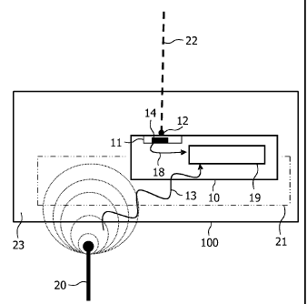
The data carrier 100 according to the invention, shown as a chip card in Fig.
2,
comprises the chip 10, and the plurality of chip sensors 11 comprises a
photosensor 14 which
detects the excitation 12 of a pulsed laser beam 22 which is modulated. The
data carrier 100
consists of card materia123 through which the pulsed laser beam 22 can
penetrate.
Conventional card materials are transparent in the NIR range of 800 to 1100 nm
so that the
excitation 12 of a pulsed laser beam 22 is specifically adjustable in this
wavelength range and
is adaptable to the requirements of processing the signal 18 in the CPU 19.
Defined
transparencies can usually be adjusted by selecting synthetic materials for
the card material
23 with the corresponding additives. Different optical excitation profiles are
created in that
the photosensor 14 detects the excitation 12 of the pulsed laser beam 22. Such
excitation
profiles are suitable for transmitting complex information to the chip 10. The
excitation of
the photosensor triggers an exception signal and thus represents an input
command for the
CPU 19. The CPU 19 is programmed in such a way that it does not only expect
the
"customary" RFID signal but also an exception signal from the photosensor 14
and thus
additively activates the chip 10 for further processes. The chip 10 stores
energy 13 as well as
information which are coupled into the chip 10 via a conventional antenna 20
and the antenna
periphery 21 so as to generate the RFID signal. It is to be noted that this
embodiment as well
as the other embodiments can also be used within the scope of contact
technologies, i.e. the
energy and information can also be transmitted via conventional contact.
CA 02590150 2007-06-08
WO 2006/061780 PCT/IB2005/054081
8
Fig. 3 shows a plurality of chip sensors 11 with a photosensor 14. The filter
material consists of the card materia123 and of a matrix 24 adjoining the card
materia123,
which matrix generates modulated luminescences, in which a pulsed laser beam
22 first
penetrates through the card materia123 and then penetrates the matrix 24.
The card materia124 is adjusted in such a way that it completely absorbs light
at wavelengths of less than 850 nm and is transparent at wavelengths of more
than 850 nm in
the NIR range. In known manner, both energy 13 and information is coupled into
and stored
on the chip 10 via an antenna 20 and an antenna periphery 21 so as to generate
the RFID
signal. Independently thereof, the pulsed laser beam 22 irradiates the matrix
24 with an
emission at 980 nm, while a UP conversion process generates a luminescence at
800 nm
(670, 550 or 430 nm). This in situ generated light (luminescence emission 31)
is incident on
the photosensor 14 and after excitation 12 triggers a signal 18 in the form of
an exception
signal, i.e. it represents an input command for the CPU 19. The luminescence
dynamics of
the UP conversion materials should be chosen to be such that the modulation of
the pulsed
laser beam 22 can be "passed on" so that a modulated luminescence reaches the
photosensor
14 and complex optical information can thus be coupled in. This means that a
simple
continuous excitation of the photosensor 14, for example, the customary
exception routine,
deactivates the chip. A defined pulsed excitation, however, triggers other
routines which lead
to complex operations in the CPU 19. The CPU 19 is programmed in such a way
that it does
not only expect the "customary" RFID signal but also defined exception signals
from the
photosensor 14 so as to reach a complex result during the processing
operation. Moreover,
the matrix 24 may be formed with special material (combinations) so that, for
example, other
optical conversion processes such as photoluminescence or invisible Stokes
luminescence
can be utilized. The matrix 24 may also be applied prior to laminating the
compound material
of the card by means of known printing techniques such as silkscreen printing,
rotogravure,
flexoprinting, offset, letter set, ink jet, thermotransfer etc. or the UC
pigment may be
incorporated when housing the chip in the epoxy resin substance so that only a
pulsed laser
beam 22 is suitable and the intensity of pulsed "NIR light" is not sufficient
to generate
adequate luminescences.
The chip sensors 11 shown on an explicitly larger scale in Fig. 4 communicate
with filter material which consists of card materia123 which is opaque at
wavelengths of less
than 800 nm and transparent at wavelengths between 800 and 1100 nm, and of a
UC
converter 25 adjoining the card materia123, as well as of an interference
filter laminate 27
adjoining the UC converter, in which the pulsed laser beam 22 penetrates
through the card
CA 02590150 2007-06-08
WO 2006/061780 PCT/IB2005/054081
9
materia123 and penetrates the UC converter 25. The UC converter 25 which is
printed on the
rear side of the card materia123 consists of, for example, ytterbium and
holmium-doped
gadolinium oxysulphide as a phosphor and is favorably formed in such a way
that the UC
radiation 26 is essentially directed downwards in the direction of the
photosensor 14 in the
form of a Si photosensor and is used as excitation. The interference filter
laminate 27 has
very sharp absorption edges so as to absorb light of wavelengths between 800
and 1100 nm.
Due to the phosphors used, the UC converter generates an emission at 550 nm.
The
luminescence can only spread in the direction of the Si photosensor where it
triggers a signal
18 which is passed on to the CPU 19. However, the laser beam required for
excitation would
be absorbed in the filter laminate layer at the latest and could thus not
activate the Si
photosensor.
Fig. 5 shows a plurality of chip sensors 11 including a photosensor 14 in the
form of a Si photosensor, with filter material consisting of a light converter
28 shifting
wavelengths and card materia123 adjoining the light converter 28, which is
transparent in a
wavelength range between 800 and 1100 nm, and in which a pulsed laser beam 22
penetrates
the light converter 28. The light converter 28 consists of (chromium)
lanthanoide-doped
yttrium vanadates (yttrium phosphates, yttrium borates) absorbing red light
and generating an
emission in the NIR range. The original excitation light is thus shifted as a
long wave. In the
simplest case, the light converter is printed by means of a conventional
printing method or
put in front as a foil additive. Other materials such as, for example,
chromium and
neodymium-doped yttrium aluminum garnets defined by the general formula
YAG:Cr,Nd
can also be used as light converters. In accordance with ISO 7810, the card
materia123
adjoining the light converter 28 is only transparent in the NIR range of 800
to 1100 nm. The
light converter 28 absorbs a pulsed laser beam 22 between 800 and 1100 nm
substantially
completely so that the pulsed laser does not reach the photosensor 14.
However, red laser
light (630-690 nm) triggers a luminescence 29 between 900 and 1000 nm
dependent on the
design of the light converter 28, which luminescence reaches the photosensor
14 through the
card materia123 and serves as excitation for the photosensor 14, further
reaching the CPU 19
as signal 18. Dependent on the light clock, for example, exceptions or defined
warm resets
are performed which are then treated as information by the operating system of
the CPU 19.
The plurality of chip sensors shown in Fig. 6 includes at least two
photosensors 14, 14a whose filter material is different, the filter material
consisting of card
materia123, in which a pulsed laser beam 22, 22a penetrates through the filter
material and
excites the photosensors 14, 14a which separately pass on a signal 18 to the
CPU 19.
CA 02590150 2007-06-08
WO 2006/061780 PCT/IB2005/054081
Based on the different equipment/doping of the card materia123, the
photosensors 14, 14a are sensitized for different wavelengths. In this
example, the card
materia123a is doped with an ytterbium phosphate and formed in such a way that
it is
transparent at wavelengths of less than 800 nm and substantially opaque at
wavelengths of
5 more than 800 nm. A photosensor 14a detects the excitation 12 of a pulsed
laser beam 22a
(wavelength 650 nm) and converts it into a signal 18 for the CPU 19, which
signal is utilized
to enable the second photosensor which can now detect the excitation 12 of a
pulsed laser
beam 22 at a wavelength of 980 nm. In this way, information is divided between
different
photosensors 14, 14a, with the result that a ternary logic can be implemented.
CA 02590150 2007-06-08
WO 2006/061780 PCT/IB2005/054081
11
LIST OF REFERENCE NUMERALS:
100 data carrier
chip
11 plurality of chip sensors
12 excitation
5 13 energy
14 photosensor
14a photosensor
temperature sensor
16 frequency sensor
10 17 sensor
18 signal
19 CPU
antenna
21 antenna periphery
15 22 pulsed laser beam
22a pulsed laser beam
23 card material
23a ytterbium phosphate card material
24 matrix
20 25 UC converter
26 UC radiation
27 interference filter laminate
28 light converter
29 luminescence
30 electromagnetic field
31 luminescence emission