Note: Descriptions are shown in the official language in which they were submitted.
CA 02590627 2007-06-07
T 46874W0/NZ/hs
Organic rectifier
The invention relates to a rectifier having at least
two organic diodes or organic field effect transistors,
which is employed for, example as a rectifier of an RFID
transponder (RFID = Radio Frequency Identification),
and to an electronic device in the form of a flexible,
multilayer film body.
RFID transponders are increasingly being employed for
providing merchandise, articles or security products
with information that can be read out electronically.
They are thus being employed for example as electronic
bar code for consumer goods, as luggage tag for=
identifying luggage or as security element that is
incorporated into the binding of a passport and stores
authentication information.
RFID transponders usually comprise two components, an
antenna and a silicon chip. The RF carrier signal
transmitted by a base station is coupled into the
antenna resonant circuit of the RFID transponder. The
silicon chip modulates an additional item of
information onto the signal fed back to the base
station. In this case, the RFID transponder is not
usually provided with an independent power source.
Power is supplied to the silicon chip by means of a
rectifier which converts the RF carrier signal coupled
into t.he antenna resonant circuit into a DC voltage and
thus additionally uses it as a power source for the
silicon chip.
In order to be able to reduce the production costs for
RFID transponders, it has been proposed to use organic
integrated circuits on the basis of organic field
effect transistors in RFID transponders. Thus,
WO 99/30432 for example, proposes using an integrated
circuit constructed substantially from organic material
in an RFID transponder, said integrated circuit
CA 02590627 2007-06-07
- 2 -
providing the function of an ID code generator. The ID
code generator is fed with a supply voltage by means of
two rectifier diodes coupled to the antenna resonant
circuit. Said rectifier diodes, downstream of which a
smoothing capacitor is connected, comprise two
specially interconnected field effect transistors.
Although the use of such specially interconnected field
effect transistors makes it possible to realize
rectifier diodes by means of organic components, if
organic field effect transistors are connected up in
this way in order to use them as rectifier diodes, the
frequency that can be picked up by said diodes is ver=y
limited since the organic field effect transistors
generally switch significantly more slowly than the RF
carrier frequency.
Typical frequency ranges used for RFID transponders are
e.g. 125 to 135 kHz, 13 to 14 MHz, 6 to 8 MHz, 20 to
40 MHz, 860 to 950 MHz or 1.7 to 2.5 GHz. However,
organic circuits are significantly slower than all
silicon-based circuits since organic semiconductors
generally have a lower charge carrier mobility than
silicon and organic field effect transistors are based
on the principle of charge carrier accumulation rather
than on the principle of charge carrier inversion. This
results in a lower switching speed in comparison with
silicon transistors and a different switching behavior
(e.g. unsuitability for AC voltage). If organic field
effect transistors as described in WO 99/30342 are thus
connected up to form a rectifier, the rectifier thus
realized switches significantly more slowly (less than
100 kHz) than the transmission frequency of the carrier
signal emitted by the base station.
It is furthermore proposed in WO 02/21612 to construct
an organic rectifier in which at least one of the pn-
doped conductive layers a conventional pn semiconductor
diode is supplemented or replaced by an organically
CA 02590627 2007-06-07
- 3 -
conductive material. It is furthermore proposed, in a
conventional metal-semiconductor diode (Schottky diode)
to replace at least one layer by an organic layer. The
choice of dimensions of the capacitive areas of this
rectifier makes it possible to set the switching
frequency of the switching rectifier. A description is
furthermore given of connecting a smoothing capacitor
downstream of a rectifier constructed from such organic
components, which smoothing capacitor smooths the DC
voltage arriving in pulsating fashion downstream of the
rectifier and is connected up in parallel with the load
resistor.
However, such organic rectifiers, too, are not very
effective at frequencies above 1 MHz. This is
attributable to the low mobility of the organic
semiconductors which are available nowadays and which
can be used in such an organic rectifier. The space
charge zone leading to the rectifying effect is no
longer built up rapidly enough at high frequencies on
account of the low charge carrier mobility in the
organic semiconductor. The efficiency of the rectifier
decreases as a result of this, which makes it more
difficult to supply downstream loads with DC voltage.
The invention is based on the object, then, of
improving the supply of downstream loads by an organic
rectifier.
This object is achieved by a rectifier for converting
an AC voltage present between two input terminals of
the rectifier into a DC voltage, which rectifier has at
least two organic diodes and/or organic field effect
transistors each having at least one electrical
functional layer composed of a semiconducting organic
material and also two or more charging or charge-
reversal capacitors which are connected up to the two
or more organic diodes or organic field effect
transistors in such a way that the charging or charge-
CA 02590627 2007-06-07
- 4 -
reversal capacitors can be charged via different
current paths. This object is furthermore achieved by
an electronic device in the form of a flexible,
multilayer film body, which electronic device has a
voltage source and a rectifier configured in the manner
described above, said rectifier being fed by the
voltage source.
In this case, the invention is based on the concept of
compensating for the low charge carrier mobility of
organic semiconductors by the interconnection with two
or more charging or charge-reversal capacitors which
are charged via different current paths of the
rectifier.
The above-described interconnection of organic
components and capacitors to form an organic rectifier
enables the rectification factor GRS = U=/U, to be
significantly increased. Experiments have thus shown,
for example, that by means of a conventional organic
half-wave rectifier at a frequency of 13.56 MHz, for
example, only approximately 5% of the AC voltage
amplitude U. fed in is converted into a DC voltage U= at
the output, which corresponds to a rectification factor
of GRV = U=/U~ = 0.05, such that downstream loads can be
supplied with DC voltage only with very great
difficult.y. Thus, t.he possibility of the rectification
of coupled-in HF signals (HF = high frequency) by means
of organic components is deemed impossible at the
present time even by many experts, the use of organic
rectifiers in RFID transponders is rejected and this is
accounted for by the low charge carrier mobility in the
organic semiconductors known at the present time. The
invention provides a remedy here and makes it possible,
through the interconnection referred to above of
organic components with charging or charge-reversal
capacitors, to provide an organic rectifier which can
supply downstream loads with the required DC voltage
even at high frequencies. In this case, possible loads
CA 02590627 2007-06-07
- 5 -
include organic logic circuits, display elements and
also conventional electronics.
In this case, the rectifier according to the invention
comprises a multilayer construction composed of two,
three or more layers, at least one layer of which is an
active layer composed of organic semiconductor
material. In this case, an organic diode realized in
this multilayer construction has a metal-semiconductor
junction or a pn junction with organic semiconductors,
in which case the metal can also be replaced by an
organic conductor. In this case, the sequence of the
individual functional layers can be arranged both
vertically and laterally. For improving the electrical
properties - e.g. injection of charge carriers -, it is
also conceivable to introduce additional interlayers
which supplement the actual functional layers.
Moreover, it is also possible for organic fi.eld effect
transistors whose gate electrode is connected to the
source or drain electrode to be used as organic diodes
in the rectifier.
Advantageous developments of the invention are referred
to in the subclaims.
In accordance with the first exemplary embodiment of
the invention, a first charging capacitor and a first
organic diode are arranged in a first conducting line
branch and a second charging capacitor and a second
or=ganic diode are arranged in a second conducting line
branch. The first and the second conducting line branch
are coupled in a parallel arrangement to the input of
the rectifier, the first and the second organic diode
being connected up in a back-to-back arrangement of the
respective anode and cathode in the first and
respectively the second conducting line branch.
CA 02590627 2007-06-07
- 6 -
In accordance with a further exemplary embodiment of
the invention, a first organic diode and a second
organic diode are connected in a back-to-back
arrangement of the respective anode and cathode via a
charge-reversal capacitor to the first input terminal
of the rectifier. The first organic diode is connected
to the second input terminal of the rectifier. The
second organic diode is connected via a charging
capacitor to the second input terminal of the
rectifier. In accordance with this arrangement, the
cathode of the first organic diode and the anode of the
second organic diode can thus be connected via the
charge-r=eversal capacitor to the first input terminal,
such that the anode of the first organic diode and the
cathode of the second organic diode are connected to
one another via the charging capacitor and the anode of
the first organic diode is connected to the second
input terminal. However, the anode of the first organic
diode and the cathode of the second organic diode can
also be connected via the charge-reversal capacitor to
the first input terminal, such that the cathode of the
first organic diode and the anode of the second organic
diode are connected to one another via the char=ging
capacitor and the anode of the first organic diode is
connected to the second input terminal.
Organic rectifiers constructed in this way have the
advantage that even with a low outlay it is possible to
achieve an increase in the supply voltage that can be
obtained on the output side. The organic rectifier can
thus be fabricated particularly cost-effectively, for
example by means of a roll-to-roll process.
A further increase in the supply voltage available on
the output side can be obtained by constructing the
rectifier from two or more stages which are connected
up to one another. Each stage of the rectifier
comprises two charging or charge-reversal capacitors
and two organic diodes or organic field effect
CA 02590627 2007-06-07
- 7 -
transistors which are connected up in such a way that
the charging or charge-reversal capacitors can be
charged via different current paths and they have in
each case two input terminals and two coupling
terminals for coupling input terminals of a further
stage.
The rectifier can in this case be construct.ed from two
or more stages of identical type which are connected up
in cascading fashion.
In one particularly advantageously constructed stage
which can be used for such cascading, the cathode of
the first organic diode and the anode of the second
organic diode are connected to the first coupling
terminal of the first stage and via the charge-reversal
capacitor to the first input terminal of the first
stage. The anode of the first organic diode and the
cathode of the second organic diode are connected to
one another via the charging capacitor. The anode of
the first organic diode is connected to the second
input terminal of the stage and the cathode of the
second organic diode is connected to the second
coupling terminal of the stage. A stage constructed in
this way is referred to hereinafter as "first stage".
Furthermore, it is also possible for the anode of the
first organic diode and the cathode of the second
organic diode to be connected to the first coupling
terminal of the stage and via the charge-reversal
capacitor to the first input terminal of the stage. The
cathode of the first organic diode and the anode of the
second organic diode are connected to one another via
the charging capacitor. The cathode of the first
organic diode is connected to the second input terminal
of the stage and the anode of the second organic diode
is connected to the second coupling terminal of the
stage. A stage constructed in this way is referred to
hereinafter as "second stage".
CA 02590627 2007-06-07
- 8 -
In the cascading of first stages or second stages, the
first and second input terminals of the foremost stage
form the first and respectively the second input
terminal of the rectifier. The coupling terminals of
the respective stage are connected to the input
terminals of the downstream stage, provided that the
respective stage does not. form the last stage of the
rectifier. The output of the rectifier is formed by the
second input terminal of the foremost stage and by the
second coupling terminal of the last stage.
Furthermore, it is also possible for first and second
stages to be connected up to one another in a
rectifier. In a rectifier constructed in this way, the
first and second input terminals of a first stage and
of a second stage are connected to one another and form
the input terminals of the rectifier. An arbitrary
number of first and second stages are subsequently
connected in the manner described above in each case to
the coupling terminals of the preceding first and
respectively second stage. The output of the rectifier
is formed by the second coupling terminal of the last
first stage and by the second coupling terminal of the
last second stage.
The advantage of such an arrangement of two different
types of stages is that - for the same supply voltage -
the DC current that can be made available to the
downstream load can be increased.
The rectification factor can furthermore be increased
by using as organic diodes organic components which
have an interlayer for lowering the parasitic
capacitance of the organic diode. As a result of the
reduction of the par=asitic capacitances of the organic
diodes, the effectiveness of the charging/charge-
reversal processes at the charging or charge-reversal
CA 02590627 2007-06-07
- 9 -
capacitors is improved and the efficiency of the
rectifier is thus increased.
In accordance with a further exemplary embodiment of
the invention, the first and/or the second input
terminal of the rectifier is connected via one or a
plurality of first organic field effect transistors to
a charge-reversal capacitor. The charge-reversal
capacitor is connected via one or a plurality of second
field effect transistors to a charging capacitor. The
one or the plurality of first and second field effect
transistors are driven by a logic circuit. In this
case, the logic circuit drives the first field effect
transistors in such a way that an alternating voltage
is applied to the charge-reversal capacitor.
Particular advantages are afforded when a rectifier=
according to the invention is used in an electronic
device having, as voltage source, a resonant circuit
comprising an antenna and a capacitor. By coupling such
an antenna resonant circuit to a rectifier accor=ding to
the invention, a DC voltage supply of downstream
electronic assemblies can be provided which can be
produced particularly cost-effectively, provides a
sufficient supply voltage and can be realized in the
form of a flexible body. Particular advantages are
furthermore afforded if an organic integrated circuit
is used as downstream electronic assembly. On account
of the par=ticular characteristic of organic integrated
circuits (e.g. very low current requirement), such a
circuit is matched particularly well to the
characteristic of the rectifier according to the
invention. Furthermore, an electronic device of this
type can be manufactured cost-effectively for mass
production applications and disposable products using a
uniform manufacturing technology.
In addition to the use of such a resonant circuit as a
voltage source, it is also possible to provide an
CA 02590627 2007-06-07
- 10 -
oscillator, for example a ring oscillator, in the
voltage source or to apply an alternating voltage to
the charging and/or charge-reversal capacitors through
corresponding driving of two or more field effect
transistors.
The invention is explained by way of example below on
the basis of a plur.-ality of exemplary embodiments with
the aid of the accompanying drawing.
Figure 1 shows a block diagram of an organic rectifier
in accordance with a first exemplary
embodiment.
Figure 2 shows a block diagram of an organic rectifier
for a further exemplary embodiment.
Figure 3 shows a block diagram of an organic rectifier
for a further exemplary embodiment.
Figure 4 shows a block diagram of a cascaded organic
rectifier for a further exemplary embodiment.
Figure 5 shows a block diagram of a cascaded organic
rectifier for a further exemplary embodiment.
Figure 6 shows a block diagram of an electronic device
with a rectifier.
Figure 7 shows a block diagr=am of an electronic device
for a further exemplary embodiment.
Figure 8 shows a block diagram of an electronic device
for a further exemplary embodiment.
The rectifiers illustrated in the figures fig. 1 to
fig. 5 each comprise a flexible, multilayer film body
having one or a plurality of electrical functional
layers. The electrical functional layers of the film
CA 02590627 2007-06-07
- 11 -
body comprise (organically) conductive layers,
organically semiconducting layers and/or organic
insulating layers which, at least partly in structured
form, are arranged one above another. Alongside these
electrical functional layers, the multilayer film body
optionally also comprises one or a plurality of carrier
layers, protective layers, decorative layers, adhesion
promoting layers or adhesive layers. The electrically
conductive functional layers preferably comprise a
conductive, structured metallization, preferably
composed of gold or silver. However, provision may also
be made for forming said functional layers from an
inorganic electrically conductive material, for example
for forming them from indium tin oxide or from a
conductive polymer, for example from polyaniline or
polypyrrole. The organically semiconducting functional
layers comprise for example conjugated polymers, such
as polythiophenes, polythienylenevinylenes or poly-
fluorene derivatives, which are applied as a solution
by spin-coating, blade coating or printing. So-called
"small molecules", i.e. oligomers such as sexithiophene
or pentacene, which are vapor-deposited by a vacuum
technique, are also suitable as organic semiconductor
layer. These organic layers are preferably applied in a
manner already structured partially or in patterned
fashion by means of a printing method (intaglio
printing, screen printing, pad printing). For this
purpose, the organic materials provided for the layers
are formed as soluble polymers, the term polymers in
this case, as already described further above, also
including oligomers and "small molecules".
In this case, the electrical functional layers of the
respective film body are configured such that they
realize the electrical circuit illustrated in the
figures fig. 1 to fig. S.
The electrical circuits described below with reference
to the figures fig. 1 to fig. 5 in each case comprise
CA 02590627 2007-06-07
- 12 -
two or more charging or charge-reversal capacitors and
two or more organic diodes.
Organic diodes are r=ealized in the multilayer film body
by a metal-semiconductor junction or a pn junction
between an n-conducting and a p-conducting semi-
conductor. In this case, the sequence of the individual
functional layers can be arranged both vertically and
laterally. Furthermore, it is possible here, in order
to improve the electrical properties - e.g. injection.
of nutrient carriers - to introduce additional inter-
layers which supplement the electrically functional
layers described above. An organic diode can thus be
realized for example by means of three successive
layers, the first layer being an electrically
conductive electrode layer that forms the cathode, the
second layer being a layer composed of an organic semi-
conductor material, and the third layer being an
electrically conductive electrode layer that forms the
anode. In this case, the organic semiconductor layer
has a layer thickness of 60 to 2000 nm, for example.
The conductive layer may comprise one of the materials
described above, that is to say either a metal or an
organically conductive material, which can be applied
by a printing process.
Furthermore, it is also possible for organic diodes to
be realized by means of a four-layer construction
comprising two electrode layers and two intervening
organic semiconductor layers, one of which has
n-conducting properties and the other of which has
p-conducting properties.
Reference is made hereinafter= to the content of
WO 02/21612 Al with regard to the construction of
organic diodes.
Furthermore, it is also possible for the organic diodes
to be formed by an organic field effect transistor
CA 02590627 2007-06-07
- 13 -
whose gate electrode is connected to the drain
electrode.
The charging or charge-reversal capacitors realized in
the multilayer film body are formed by two electrically
conductive layers and an intervening insulating layer.
The electrically conductive layers may comprise one of
the materials described above, may thus comprise for
example metallic layers or organic electrically
conductive layers, which have been applied by means of
a printing method. In this case, the charging or
charge-reversal capacitors have a capacitance within
the range of 1 pF to 2 nF.
Figure 1 shows a rectifier 1 comprising two organic
diodes OD1 and OD2 and two charging capacitors Cl and
C2. The rectifier 1 has an input El with input
terminals E11 and E12 and an output Al. The input
terminal E11 is connected to the cathode of the organic
diode OD1 and to the anode of the organic diode OD2.
The anode of the organic diode OD1 is connected via the
charging capacitor Cl and the cathode of the organic
diode OD2 is connected via the charging capacitor C2 to
the input terminal E12. The output voltage is tapped
off between the cathode of the organic diode OD2 and
the anode of the organic diode OD1.
The input AC voltage present at the input El is
r=ectified by means of the organic diode OD1 in a
negative voltage across the charging capacitor Cl and
rectified by means of the organic diode OD2 to form a
positive voltage. The output-side DC voltage present at
the output Al thus corresponds to the sum of the
magnitudes of the voltages across Cl and C2.
Figure 2 shows a rectifier 2 having a charge-reversal
capacitor Cl, a charging capacitor C2 and two organic
diodes OD1 and OD2. The rectifier 2 has an input E2
with two input terminals E21 and E22, an output A2 and
CA 02590627 2007-06-07
- 14 -
two coupling terminals B21 and B22. The charge-reversal
capacitor Cl is connected at one end to the input
terminal E21 and at the other end to the coupling
terminal B21, the cathode of the organic diode OD1 and
the anode of the organic diode OD2. The charging
capacitor C2 is connected at one end to the anode of
the organic diode OD1 and the input terminal E22 and at
the other end to the cathode of the organic diode OD2
and the coupling terminal B22. The output voltage is
tapped off via the charging capacitor C2. The input AC
voltage applied to the input E2 is rectified by means
of the organic diode OD1 to form a voltage across the
charge-rever=sal capacitor Cl. During the positive half-
cycle of the input AC voltage, the positive charges
situated on the charge-reversal capacitor Cl can be
transported via the organic diode 0D2 to the charging
capacitor C2. An increased positive voltage thus builds
up across the charging capacitor C2, and can be tapped
off via the output A2.
Figure 3 shows a rectifier 3 having a charge-reversal
capacitor Cl, two organic diodes OD1 and OD2 and a
charging capacitor C2. The rectifier 3 has an input E3
with two input terminals E31 and E32, an output A3 and
two coupling terminals B31 and B32. The charge-reversal
capacitor Cl is connected at one end to the input
terminal E31 and at the other, end to the anode of the
organic diode OD1, the cathode or organic diode OD2
and the coupling terminal B31. The charging capacitor
C2 is connected at one end to the cathode of the
organic diode OD1 and to the input terminal E32 and is
connected at the other end to the anode of the organic
diode OD2 and the coupling terminal B32. The output
voltage is tapped off via the charging capacitor C2. In
contrast to the rectifier 2, in the case of the
rectifier 3, during the negative half-cycle of the
input AC voltage, the negative charge situated on the
charge-reversal capacitor Cl is transpor=ted via the
organic diode OD2 to the char=ging capacitor C2. An
CA 02590627 2007-06-07
- 15 -
increased negative voltage thus builds up across the
charging capacitor C2, and is tapped off via the output
A3.
The rectifiers illustrated in figure 2 and figure 3 can
be cascaded in a cascaded arrangement in each case to
form a multistage organic or printable rectifier.
Figure 4 shows an example of such a rectifier. Figure 4
shows a rectifier 4 constructed from two or more
stages, of which two stages S41 and S42 are shown in
figure 4. The stages S41 and S42 are in each case
constructed like the rectifier 2 according to figure 2.
The stage S41 thus has an input with two input
terminals in E41 and E42, an output A41 and two
coupling terminals B41 and B42. The stage S42 has two
input terminals E43 and E44, an output A42 and two
coupling terminals B43 and B44. The input terminals and
coupling terminals of the stages S41 and S42 are
connected up to a charge-reversal capacitor, a charging
capacitor and two organic diodes as shown in figure 2.
The input terminals E41 and E42 of the first stage of
the rectifier 4 form an input of the rectifier 4, which
is designated by E4 in figure 4. The input terminals of
the downstream stage are respectively connected to the
coupling terminals of one stage of the rectifier 4. The
output-side DC voltage thus results from the sum of the
output voltages at the outputs of the individual
stages, such that the voltage present at the output A4
of the rectifier 4 is increased further.
It is also possible to construct the rectifier 4 by
means of a cascaded arrangement of individual stages
which are each constructed like the rectifier 3
according to figure 3.
Figure 5 shows a rectifier 6 composed of differently
constructed individual stages. The rectifier 6 has, on
CA 02590627 2007-06-07
- 16 -
the one hand, two or more stages which are each
constructed like the rectifier 2 according to figure 2.
Of said stages, figure 5 shows two stages S61 and S62
having input terminals E61 and E62 and respectively E63
and E64, coupling terminals B61 and B62 and
respectively B63 and B64 and outputs A61 and
respectively A62. These stages, as already explained
with reference to figure 4, are connected up to one
another in a cascaded arrangement in such a way that
the input terminals of the downstream stage are
connected up to the coupling terminals of the preceding
stage.
The rectifier 6 further=more has two or more stages
configured like the rectifier 3 according to figure 3.
Of said stages, figure 5 shows two stages S63 and S64
having input terminals E61 and E62 and respectively E65
and E66, coupling terminals B65 and B66 and
respectively B67 and B68 and outputs A63 and
respectively A64. Said stages are likewise connected up
to one another in cascading fashion, as explained in
figure 4, in such a way that the input terminals of the
downstream stage are connected to the coupling
terminals of the preceding stage. The input terminals
of the stages S61 and S63 are in each case connected to
the input E6 of the rectifier 6, such that the positive
output voltages present at the outputs of the stages
S61 and S62 are added to the negative voltages present
at the outputs of the stages S63 and S64 and an
increased output voltage is thus present at the output
A6 of the rectifier 6.
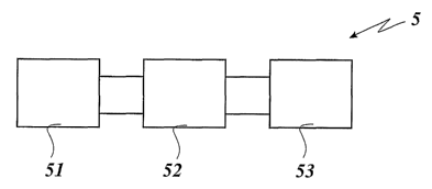
Figure 6 shows an electronic device 5 having a power
source 51, a rectifier 52 and an electronic circuit 53
fed by the rectifier 52. The electronic device 5 is an
RFID transponder. The electronic device 5, as already
explained with reference to the figures fig. 1 to
fig. 5, is constructed from a multilayer flexible film
body having two or more electrical functional layers.
CA 02590627 2007-06-07
- 17 -
In this case, the power source 51 is formed by an
antenna resonant circuit comprising an antenna and a
tuning capacitor. The rectifier 52 is formed by a
rectifier constructed like one of the rectifiers 1, 2,
3, 4 or 6 according to figure 1 to figure 5.
The electronic circuit 53 is an ID code generator
constructed from one or a plurality of active or-
passive organic components, preferably organic field
effect transistors.
However, it is also possible for the electronic circuit
53 to provide a different function or to be replaced by
an output unit, for example to be formed by an organic
light emitting diode or a liquid crystal display.
Figure 7 shows an electronic device 7 serving for
supplying an organic or printable logic circuit. The
electronic device 7 has a voltage source 71, a logic
circuit 72, a plurality of organic field effect
transistors OF1, OF2, OF3, OF4, two charge-reversal
capacitors CS1 and CS2 and a charging capacitor CO. The
two charge-reversal capacitors CS1 and CS2 in each case
have the capacitance of the charging capacitor CO and
can also be replaced by a capacitor having twice the
capacitance or a greater capacitance. In this case, the
logic cir-cuit is fed by the output voltage present at
an output A7 of the electronic device.
The voltage source 71 supplies an arbitrary AC voltage
with or without a DC voltage component. The voltage
source 71 can thus be formed for example by an antenna
resonant circuit according to figure 6 and/or by a
battery, for example a printed battery or storage
battery. The logic circuit 72 comprises one or a
plurality of organic field effect transistors connected
up to one another. It controls a switching matrix
comprising the organic field effect transistors OF1 to
OF4. Through suitable construction and driving of the
CA 02590627 2007-06-07
- 18 -
switching matrix, a DC voltage arises as a result of
the charging and charge-reversal processes at the
output of the switching matrix. The logic circuit 72
thus drives the organic field effect transistors OF1 to
OF4 for example in such a way that during the positive
half-cycle, the field effect transistors OF1 and OF2
are turned on and the field effect transistors OF3 and
OF4 are turned off. Dur=ing a further positive half-
cycle, the organic field effect transistors OF3 and OF4
are then turned on and the organic field effect
transistors OF1 and OF2 are turned off.
Furthermore, it is also possible to provide even
further organic field effect transistors in the
switching matrix in order thus for example to utilize
the negative half-cycle of the voltage source 71.
Furthermore, it is also possible in this way to
increase a DC voltage present on the input side at the
switching matrix.
Figure 8 shows an electronic device having a voltage
source 81, an oscillator 82 and a rectifier 83. The
rectifier 83 has an input with two input terminals A81
and A82 and an output 8. The rectifier 83 is
constructed like one of the rectifiers 1, 2, 3, 4 and 6
according to figure 1 to figure 5.
The voltage source 81 is a DC voltage source, for
example a battery. Furthermore, it is also possible for
the voltage source 81 to be a rectifier which is
constructed according to the figures fig. 1 to fig. 5
and which is fed by an AC voltage source, for example
an antenna resonant circuit.
The oscillator 82 is a printable ring oscillator which
converts the input voltage into an AC voltage,
preferably having a frequency of less than 1 MHz. The
rectifier 83 is a rectifier which is constructed like
one of the rectifiers according to the figures fig. 1
CA 02590627 2007-06-07
- 19 -
to fig. 5. By means of this construction, the voltage
is effectively rectified into a DC voltage present at
the output 8.
It is also possible for a rectifier according to the
figures fig. 1 to fig. 5 also to be combined with a
rectifier according to figure 7 in this way, that is to
say for= a rectifier according to the figures fig. 1 to
fig. 5 together with an AC voltage source to form the
voltage source 71 according to figure 7. An arrangement
of this type makes it possible to obtain for example an
impedance matching to the electronic circuit supplied
by the rectifier.