Note: Descriptions are shown in the official language in which they were submitted.
CA 02590659 2007-06-14
WO 2006/069321 PCT/US2005/046807
1
TRANSMIT POWER REDUCTION FOR A WIRELESS
DEVICE WITH MULTIPLE TRANSMIT SIGNAL PATHS
BACKGROUND
I. Field
[0001] The present invention relates generally to communication, and more
specifically to techniques for transmitting data by a wireless device.
II. Background
[0002] In a wireless communication system, a radio frequency (RF) signal
transmitted by a wireless device (e.g., a cellular phone) may reach a base
station via
multiple signal paths. These signal paths may include a line-of-sight path and
reflected
paths, which are created by reflections of radio waves in the environment. The
base
station may thus receive multiple instances of the transmitted RF signal. Each
received
signal instance is obtained via a different signal path and has a complex gain
and a
propagation delay determined by that signal path. The received signal
instances may
add constructively at the base station and produce a received signal having a
larger
magnitude. Conversely, the received signal instances may add destructively and
produce a received signal having a smaller magnitude. Different received
signal levels
may thus be obtained depending on reinforcement or cancellation of the
received signal
instances. Reinforcement is usually not problematic. However, cancellation may
cause
the received signal level to drop by a large amount, e.g., by up to 40
decibels (dB). The
received signal is said to be in a "fade" when attenuated by a large amount
due to
cancellation.
[0003] Some wireless communication systems, such as Code Division Multiple
Access (CDMA) systems, utilize power control to mitigate the deleterious
effects of
fading. With power control, the transmit power of the wireless device is
adjusted either
up or down as needed to achieve a target signal-to-total-noise ratio (SNR) at
the base
station. If the base station detects that the received SNR for the wireless
device drops
below the target SNR, e.g., due to changes in the wireless environment, then
the base
station sends transmit power control (TPC) cornmands to direct the wireless
device to
increase its transmit power. The wireless device may vary its transmit power
over a
CA 02590659 2007-06-14
WO 2006/069321 PCT/US2005/046807
2
wide range in order to maintain the received SNR at or near the target SNR.
For
example, if a fade causes the received signal at the base station to drop by
20 dB, then
the wireless device would be instructed to increase its transmit power by
approximately
20 dB (or 100 times higher) in order to maintain the desired SNR at the base
station.
[0004] Many wireless devices are portable and powered by internal batteries.
The
use of high transmit power to combat fading depletes battery power, which
shortens talk
time. There is therefore a need in the art for techniques to reduce transmit
power and
extend talk time for such a portable wireless device.
SUlVIMARY
[0005] A wireless device equipped with multiple (e.g., two) antennas and
capable of
transmitting in a manner to reduce transmit power on average is described
herein. Each
antenna interacts with the wireless environment in a different manner and is
used to
provide diversity. The multiple antennas may be of different designs/types
(e.g., a
dipole antenna and a patch antenna) to achieve different scattering effects.
The wireless
device also has one transmit signal path for each antenna. Each transmit
signal path
generates an RF output signal for transmission from the associated antenna.
The RF
output signals for the multiple antennas may have the same or different signal
levels.
[0006] The wireless device controls the operation of one or more designated
transmit signal paths to achieve a larger received signal level at a receiving
base station.
The control of the designated transmit signal path(s) is in addition to the
gain or
transmit power adjustment that is normally performed by the wireless device in
response to TPC commands received from the base station for power control. For
example, the wireless device may autonomously control the designated transmit
signal
path(s) without relying on any feedback from the base station. The wireless
device may
also control the designated transmit signal path(s) based on the received TPC
commands. For both autonomous and feedback-based control, the wireless device
may
selectively enable and disable each transmit signal path, vary the phase
and/or gain of
each transmit signal path, and so on. In any case, the larger received signal
level at the
base station due to the varied operation of the designated transmit signal
path(s) allows
the wireless device to transmit at a lower transmit power level on average,
which then
reduces power consumption and extends talk time for the wireless device.
CA 02590659 2007-06-14
WO 2006/069321 PCT/US2005/046807
3
[0007] Various aspects and embodiments of the invention are described in
fixrther
detail below.
BRIEF DESCRIPTION OF THE DRAWINGS
[0008] The features and nature of the present invention will become more
apparent
from the detailed description set forth below when taken in conjunction with
the
drawings in which like reference characters identify correspondingly
throughout.
[0009] FIG. 1 shows scattering effect on a signal transmission.
[0010] FIG. 2 shows a block diagram of a wireless device and a base station.
[0011] FIG. 3 shows an embodiment of a transmitter unit at the wireless
device.
[0012] FIG. 4 shows another embodiment of the transmitter unit.
[00131 FIG. 5 shows yet another embodiment the transmitter unit.
[0014] FIG. 6 shows a transmit RF integrated circuit (TX RFIC) within the
transmitter unit in FIG. 5.
[0015] FIG. 7 shows a process to control the operation of multiple transmit
signal
paths.
DETAILED DESCRIPTION
[0016] The word "exemplary" is used herein to mean "serving as an example,
instance, or illustration." Any embodiment or design described herein as
"exemplary"
is not necessarily to be construed as preferred or advantageous over other
embodiments
or designs.
[0017] FIG. 1 shows the effect of scattering on a signal transmission from a
single
transmit antenna 112 at a wireless device 110 to a single receive antenna 152
at a base
station 150. Scattering refers to the interaction between the transmit antenna
and the
wireless environment (or radio channel). The scattering results in an RF
output signal
sent from the transmit antenna being received via reflected (or scattered)
paths as well
as possibly line-of-sight (or direct) path. The multiple received signal
instances for the
different signal paths may add constructively or destructively at the receive
antenna.
The received signal may be larger if the received signal instances reinforce
one another
or attenuated if the received signal instances cancel one another, depending
on the path
lengths and signal phase upon arrival. The interaction between the transmit
antenna and
CA 02590659 2007-06-14
WO 2006/069321 PCT/US2005/046807
4
the wireless environment determines the set of signal paths for the
transmitted RF signal
and hence the received signal strength at the receive antenna.
[0018] Different transmit antennas may be used for transmit antenna 112 and
these
different transmit antennas would generally experience different scattering
effects in the
same wireless environment. The transmit antennas may be considered to be
"different"
if they are of different antenna designs or types and/or have different beam
patterns,
different locations, different polarizations, and/or some other different
characteristics.
In general, transmit antennas that are more different from one another tend to
experience more different scattering effects. Transmit antennas are considered
to be de-
correlated (i.e., uncorrelated) or having low correlation if they interact
with the wireless
environment in significantly different ways.
[0019] The received signal at the base station has a signal level that is
determined
by the transmit antenna used for transmission and the wireless environment.
The base
station may obtain a different received signal level for each different
transmit antenna
used for transmission in the same wireless environment due to the different
scattering
effect achieved by the transmit antenna. Different received power levels
obtained by
the base station for different individual transmit antennas are de-correlated
if these
transmit antennas are de-correlated and the wireless environment produces
sufficient
scattering due to path delay.
[0020] The above description assumes the use of one transmit antenna 112 for
data
transmission. To improve performance, multiple transmit antennas may be used
to
create multiple different and preferably de-correlated sets of received signal
instances at
the base station, one set for each transmit antenna. The multiple transmit
antennas may
be selectively enabled and disabled and/or the signals sent from these
transmit antennas
may be adjusted in amplitude and/or phase such that all of the received signal
instances
at the base station combine to produce a larger received signal. The different
interactions between the different transmit antennas and the wireless
environment (and
hence different scattering effects) are relied upon to improve the received
signal level.
This is in contrast to conventional beamfonning which attempts to form an
antenna
beam and steer a signal transmission toward the receive antenna.
[0021] In the following description, a "channel configuration" refers to a
given set
of one or more transmit antennas operating in a given wireless environment.
Different
channel configurations may be obtained with different individual antennas,
different
CA 02590659 2007-06-14
WO 2006/069321 PCT/US2005/046807
combinations of antennas, different adjustments of the signals sent from
multiple
antennas, and so on. A "transmit signal path" refers to a collection of
circuit blocks
used to generate an RF output signal (RFout) for one antenna. One transmit
signal path
is provided for each antenna. However, multiple transmit signal paths may
share some
common circuit blocks. Each transmit signal path generally covers all of the
signal
processing/conditioning from analog baseband to RF.
[0022] FIG. 2 shows a block diagram of an embodiment of a wireless device 210
and a base station 250. For this embodiment, wireless device 210 is equipped
with two
antennas 230a and 230b, and base station 250 is equipped with a single antenna
252. In
general, wireless device 210 may be equipped with any number of antennas, and
base
station 250 may also be equipped with any number of antennas.
[0023] On the reverse link (or uplink), a transmit (TX) data processor 212
receives
and processes traffic data and generates one or more streams of data chips.
The
processing by TX data processor 212 is system dependent and may include, e.g.,
encoding, interleaving, symbol mapping, and so on. For a CDMA system, the
processing typically fixrther includes channelization and spectral spreading.
TX data
processor 212 also converts each stream of data chips into a corresponding
analog
baseband signal. A transmitter unit 220 receives and conditions (e.g.,
amplifies, filters,
and frequency upconverts) the baseband signals from TX data processor 212 and
generates an RF output signal for each antenna used for data transmission. The
RF
output signals are routed through a duplexer unit 222 and transmitted via
antennas 230a
and 230b.
[0024] At base station 250, the RF signals transmitted by wireless device 210
are
received by antenna 252, routed through a duplexer 254, and provided to a
receiver unit
256. Receiver unit 256 conditions (e.g., filters, amplifies, and frequency
downconverts)
the received signal, digitizes the conditioned signal, and provides a stream
of data
samples. A receive (RX) data processor 260 processes the data samples and
provides
decoded data. The processing by RX data processor 260 is complementary to the
processing by TX data processor 212 and may include, e.g., despreading, de-
channelization, symbol demapping, deinterleaving, and decoding.
[0025] For power control of wireless device 210, an SNR estimator 262
estimates
the received SNR for wireless device 210, e.g., based on a pilot transmitted
by the
wireless device. A controller 270 compares the received SNR against a target
SNR for
CA 02590659 2007-06-14
WO 2006/069321 PCT/US2005/046807
6
wireless device 210 and generates TPC commands based on the result of the
comparison. Each TPC command may be either an UP command to direct wireless
device 210 to increase its transmit power (e.g., by a predetermined amount) or
a DOWN
command to direct wireless device 210 to decrease its transmit power.
Controller 270
typically adjusts the target SNR to achieve a target packet/frame error rate
for wireless
device 210. The TPC commands for wireless device 210 as well as other data are
processed by a TX data processor 280, conditioned by a transmitter unit 282,
routed
through duplexer 254, and transmitted via antenna 252.
[0026] At wireless device 210, the RF signal transmitted by base station 250
is
received by antennas 230a and 230b, routed through duplexer unit 222,
conditioned and
digitized by a receiver unit 232, and processed by an RX data processor 234 to
recover
the TPC commands sent by base station 250 for wireless device 210. A
controller 240
receives the TPC commands and controls the processing by TX data processor 212
and
the operation of transmitter unit 220. For example, controller 240 may
generate control
signals that vary the operation of transmitter unit 220 for transmission on
the reverse
link. The control signals may be generated (1) based on the received TPC
commands
and/or some other feedback from base station 250 or (2) autonomously by
wireless
device 210 without any feedback, as described below.
[0027] Controllers 240 and 270 also direct the operation of various processing
units
within wireless device 210 and base station 250, respectively. Memory units
242 and
272 store data and program codes for controllers 240 and 270, respectively.
[0028] The TPC commands represent one form of feedback that is readily
available
at wireless device 210 and which may be used to deduce the current channel
condition.
Wireless device 210 may detect a fade if a high percentage of UP commands are
received from base station 250. However, other forms of feedback from base
station
250 may also be used to deduce the current channel condition.
[0029] At wireless device 210, antenna 230a may be considered as the main
antenna, and antenna 230b may be considered as the secondary or diversity
antenna.
Antennas 230a and 230b may be implemented with the same or different antenna
designs. If antennas 230a and 230b are of the same design/type, then different
scattering effects may be achieved by placing these antennas at different
locations
and/or with different orientations. However, improved performance may be
achieved if
CA 02590659 2007-06-14
WO 2006/069321 PCT/US2005/046807
7
antennas 230a and 230b are of different designs/types and have different
antenna
patterns, different polarizations, and/or some other different
characteristics.
[0030] For example, antenna 230a may be implemented as a dipole antenna, and
antenna 230b may be implemented as a patch antenna. A dipole antenna is also
called a
whip antenna, and a common example is a pullout antenna often used for
cellular
phones. An exemplary design of a dipole antenna is described in U.S. Patent
No.
6,239,755, entitled "Balanced, Retractable Mobile Phone Antenna," issued May
29,
2001. A patch antenna is also called a planar antenna and is typically
fabricated on a
printed circuit board. An exemplary design of a patch antenna is described in
U.S.
Patent No. 6,559,809, entitled "Planar Antenna for Wireless Communications,"
issued
May 6, 2003. An exemplary antenna assembly with two different types of
antennas (a
sleeve dipole antenna and a quadrifilar helix antenna) is described in U.S.
Patent No.
6,720,929, entitled "Compact Dual Mode Integrated Antenna System for
Terrestrial
Cellular and Satellite Telecommunications," issued April 13, 2004. Other,
types of
antenna may also be used for antennas 230a and 230b. For example, antennas
230a and
230b may be implemented with flat coils, patches, microstrip antennas,
stripline
antennas, printed dipoles, inverted F antennas (which are special cases of
patch
antennas), planar inverted F antennas (PIFA), polarized patches, plate
antennas (which
are irregularly shaped, flat antennas with no ground plane), and so on.
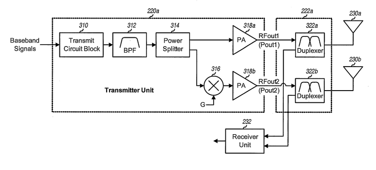
[0031] FIG. 3 shows a block diagram of a transmitter unit 220a, which is an
embodiment of transmitter unit 220 in FIG. 2. Within transmitter unit 220a, a
transmit
circuit block 310 receives the baseband signals and generates a modulated
signal.
Transmit circuit block 310 typically includes amplifiers, mixers, filters, and
so on, and
may be implemented within an RF integrated circuit (RFIC) and/or with discrete
circuit
components. A bandpass filter (BPF) 312 filters the modulated signal and
provides a
filtered modulated signal. A power splitter 314 splits the filtered modulated
signal,
provides a first RF modulated signal to a power amplifier (PA) 318a, and
provides a
second RF modulated signal to a circuit element 316. Power splitter 314 may be
implemented with a coupler or some other type of circuit. The first and second
RF
modulated signals may have the same or different signal levels. For example,
the
second RF modulated signal may be smaller than the first RF modulated signal
by 3 dB,
6 dB, 10 dB, or some other amount.
CA 02590659 2007-06-14
WO 2006/069321 PCT/US2005/046807
8
[0032] Circuit element 316 multiplies the second RF modulated signal with a
complex gain G and provides a scaled RF modulated signal to a power amplifier
318b.
Circuit element 316 may scale the amplitude and/or rotate the phase of the
second RF
modulated signal to generate the scaled RF modulated signal. Power amplifier
318a
amplifies the first RF modulated signal and provides a first RF output signal
(RFoutl),
which is routed through a duplexer 322a and transmitted from antenna 230a.
Similarly,
power amplifier 318b amplifies the scaled RF modulated signal and provides a
second
RF output signal (RFout2), which is routed through a duplexer 322b and
transmitted
from antenna 230b. Power amplifiers 318a and 318b may have the same or
different
gains. For example, power amplifier 318a may be designed to provide more gain
and
higher RF output signal level than power amplifier 318b (e.g., 25 dB gain for
power
amplifier 318a versus 15 dB gain for power amplifier 318b). The RF output
signal level
from power amplifier 318a is Poutl and the RF output signal level from power
amplifier
318b is Pout2, where Poutl may or may not be equal to Pout2.
[0033] The main transmit signal path includes all of the circuit blocks from
transmit
circuit block 310 up to antenna 230a, including power amplifier 318a and
duplexer
322a. The diversity transmit signal path includes all of the circuit blocks
from transmit
circuit block 310 up to antenna 230b, including circuit element 316, power
amplifier
318b, and duplexer 322b. Transmit circuit block 310, bandpass filter 312, and
power
splitter 314 are common to and shared by both the main and diversity transmit
signal
paths. The main transmit signal path may be designed to be compliant with
applicable
system requirements such as, e.g., power and linearity requirements imposed by
the IS-
98 standard for CDMA. The diversity transmit signal path may or may not be
compliant with all of the system requirements. For example, the diversity
transmit
signal path may be designed to meet all IS-98 specifications except for the
maximum
output power requirement of +23 dBm (e.g., the diversity transmit signal path
may
provide a maximum output power of only +12 dBm). If the diversity transmit
signal
path is not fully spec-compliant and/or if the second RF output signal level
is smaller
than the first RF output signal level, then power amplifier 318b may not need
to have
the same power and linearity performance as power amplifier 318a. In this
case, power
amplifier 318b may be designed with fewer amplifier stages and/or to consume
less
power and have lower cost. It may also be possible to omit power amplifier
418b from
the diversity transmit signal path. Duplexer 322b may also have relaxed
requirements.
CA 02590659 2007-06-14
WO 2006/069321 PCT/US2005/046807
9
[0034] Antenna 230a may be of a first type (e.g., a dipole antenna) and
antenna
230b may be of a second type (e.g., a patch antenna), as described above. If
antennas
230a and 230b are de-correlated, then when the channel for one of the antennas
is faded,
the channel for the other antenna may not be faded. By adjusting the relative
phase
and/or amplitude of the two RF output signals, a larger received signal may be
obtained
by base station 250 with the same or lower transmit power from wireless device
210.
Circuit element 316 is used to adjust the complex gain (i.e., phase and/or
amplitude) of
the second RF output signal transmitted from diversity antenna 230b and may be
implemented with a multiplier, a programmable delay element, or some other
type of
circuit. The adjustment of the complex gain for the diversity transmit signal
path may
be performed in various manners.
[0035] In one embodiment, wireless device 210 autonomously adjusts the complex
gain for the second transmit signal path without any feedback from base
station 250. In
a first adjustment scheme, wireless device 210 systematically sweeps the phase
of the
second RF output signal. This may be achieved by multiplying the second RF
modulated signal from power splitter 314 with a complex gain of e'2"'"lN for
each time
interval n. The duration of each time interval may be defined to be shorter
than the
expected duration of a fast fade, so that that the second RF output signal can
be adjusted
through the fade. The entire 360 is swept over N time intervals, where N may
be any
value greater than one. In a second adjustment scheme, the second RF modulated
signal
is multiplied with a pseudo-random phase of e'Z"'p(")1N for each time interval
n, where
p(n) is a pseudo-random value between 0 and N, i.e., 0<_ p(n) < N. In a third
adjustment scheme, the diversity transmit signal path is cycled between an ON
state
(enabled) and an OFF state (disabled) by alternately multiplying the second RF
modulated signal with gains of G=1 and G = 0, respectively. The second RF
modulated signal may also be multiplied with some other complex values that
may be
systematically or pseudo-randomly selected.
[0036] In another embodiment, wireless device 210 adjusts the complex gain for
the
diversity transmit signal path based on feedback from base station 250. This
feedback
may be in the form of the TPC commands sent by base station 250 for power
control of
wireless device 210. Wireless device 210 may detect for a drop in the received
signal
level at base station 250 based on the received TPC commands. For example,
wireless
CA 02590659 2007-06-14
WO 2006/069321 PCT/US2005/046807
device 210 may deduce that the current channel configuration is in a fade if a
predetermined number of consecutive UP commands is received from base station
250,
if a predetermined percentage (or higher) of TPC commands received within a
certain
time window is UP commands, and so on. Wireless device 210 may then adjust the
complex gain for the second transmit signal path whenever a fade is detected
based on
the received TPC commands. If antennas 230a and 230b are de-correlated, then
there is
good probability that the new channel configuration will be better than the
prior channel
configuration. Wireless device 210 may continue to adjust the complex gain
until the
distribution of TPC commands is deemed to be back to normal. Wireless device
210
may adjust the complex gain at a rate that is slower than the TPC command rate
to give
each complex gain setting sufficient time to take effect.
[0037] FIG. 4 shows a block diagram of a transmitter unit 220b, which is
another
embodiment of transmitter unit 220 in FIG. 2. Within transmitter unit 220b, a
transmit
circuit block 410, a bandpass filter 412, and a power splitter 414 process the
baseband
signals as described above for FIG. 3 and provide first and second RF
modulated signals
to power amplifiers 418a and 418b, respectively. Power amplifier 418a
amplifies the
first RF modulated signal and provides the first RF output signal, which is
routed
through a duplexer 422a and transmitted from antenna 230a. Similarly, power
amplifier
418b amplifies the second RF modulated signal and provides the second RF
output
signal, which is routed through a duplexer 422b and a diplexer 424 and
transmitted from
antenna 230b. The first RF output signal level is Poutl and the second RF
output signal
level is Pout2. The first and second RF output signals may have the same or
different
signal levels. For example, the second.RF output signal may have a lower
signal level
than the first RF output signal. The lower level for the second RF output
signal may be
obtained by (1) generating the second RF modulated signal to be smaller than
the first
RF modulated signal and/or (2) using a lower gain for power amplifier 418b
than for
power amplifier 418a.
[0038] Power amplifier 418a and duplexer 422a are part of the main transmit
signal
path. Power amplifier 418b, duplexer 422b, and diplexer 424 are part of the
diversity
transmit signal path. A first control signal (Ctrll) is provided to power
amplifier 418a
and used to control the operation of power amplifier 418a. A second control
signal
(Ctrl2) is provided to power amplifier 418b and used to control the operation
of power
amplifier 418b. Each control signal may selectively enable or disable the
associated
CA 02590659 2007-06-14
WO 2006/069321 PCT/US2005/046807
11
power amplifier, adjust the phase and/or gain of the associated power
amplifier, and/or
adjust the operation of the associated power amplifier in some other manner.
Each
control signal may be generated based on the TPC commands received from base
station 250. However, the Ctrll and Ctr12 signals may be generated in
different
manners, as described below. Wireless device 210 may control the main and
diversity
transmit signal paths in various manners.
[0039] In an embodiment, the main transmit signal path is enabled whenever
wireless device 210 is transmitting, and the diversity transmit signal path is
selectively
enabled and disabled based on feedback from base station 250. For this
embodiment,
the Ctrll signal is used to adjust the transmit power level of the first RF
output signal
from power amplifier 418a. The Ctrll signal may be generated in the normal
manner
based on the TPC commands received from base station 250 and may (1) increase
the
gain of power a.mplifier 418a by a predetermined amount for each UP command
and (2)
decrease the gain of power amplifier 418a by a predetermined amount for each
DOWN
command. The Ctrl2 signal may also be generated based on the received TPC
commands to achieve good performance at base station 250. In a first
adjustment
scheme, the Ctr12 signal toggles power amplifier 418b between the ON state
(enabled)
and the OFF state (disabled) whenever a fade is detected based on the received
TPC
commands. A fade may be detected as described above for FIG. 3. Different
channel
configurations, and hence different received signal levels at the base
station, are
obtained with the diversity transmit signal path enabled and disabled. In a
second
adjustment scheme, the Ctrl2 signal enables power amplifier 418b if a fade is
detected
and disables power amplifier 418b if good channel condition is detected. Good
channel
condition may be detected, e.g., if a predetermined number of consecutive DOWN
commands is received from base station 250, if a predetermined percentage (or
higher)
of TPC commands received within a certain time window is DOWN commands, and so
on.
[0040] In another embodiment, wireless device 210 cycles through the main and
diversity transmit signal paths based on feedback from base station 250.
Wireless
device 210 may initially enable the main transmit signal path for transmission
on the
reverse link. Wireless device 210 may then enable both the main and diversity
transmit
signal paths if a fade is detected, then enable just the diversity transmit
signal path if
another fade is detected, then enable just the main transmit signal path if
another fade is
CA 02590659 2007-06-14
WO 2006/069321 PCT/US2005/046807
12
detected, and so on. For this embodiment, each detected fade results in a
different
channel configuration being selected for transmission. The main and diversity
transmit
signal paths may be enabled and disabled in a predetermined order (e.g., as
described
above) or in a pseudo-random manner.
[0041] As noted above, the second RF output signal for the diversity transmit
signal
path may be lower in amplitude than the first RF output signal for the main
transmit
signal path. If a fade causes the received signal level at the base station to
drop by 20
dB, then performance may be improved even if the second RF output signal is 3
dB, 6
dB, or even 10 dB lower than the first RF output signal. Furthermore, the
actual
transmit power level used by the wireless device is often lower than the
maximum
transmit power specified by the system. For example, although IS-98 specifies
a
maximum transmit power level of 23 dBm at the antenna, the actual transmit
power
level used by the wireless device is often between a nominal range of 5 dBm
and 10
dBm for most operating scenarios. The actual transmit power level is rarely at
the
maximum or minimum power level specified by the system and, instead, is within
the
nominal range for much of the time. These operating characteristics may be
exploited
to simplify the implementation of the transmitter unit at the wireless device.
[0042] FIG. 5 shows a block diagram of a transmitter unit 220c, which is yet
another embodiment of transmitter unit 220 in FIG. 2. Within transmitter unit
220c, a
transmit RF integrated circuit (TX RFIC) 510 receives and processes the
baseband.
signals and provides the first and second RF modulated signals. A bandpass
filter 512
filters the first RF modulated signal and provides a filtered modulated
signal. A power
amplifier 518 amplifies the filtered modulated signal and provides the first
RF output
signal to duplexer 422a. The second RF modulated signal is used as the second
RF
output signal and is provided directly to duplexer 422b. The first RF output
signal level
is Poutl and the second RF output signal level is Pout2, where Poutl is
typically higher
than Pout2 due to power amplifier 518.
[0043] The Ctrll signal is provided to power amplifier 518 and used to control
the
operation of power amplifier 518 for the main transmit signal path. The Ctrl2
signal is
provided to TX RFIC 510 and used to control the operation of TX RFIC 510 for
the
diversity transmit signal path. Each control signal may selectively enable or
disable the
associated transmit signal path, adjust the phase and/or gain of the
associated transmit
signal path, and/or alter the operation of any circuit element within the
associated
CA 02590659 2007-06-14
WO 2006/069321 PCT/US2005/046807
13
transmit signal path. Each control signal may be generated based on the TPC
commands received from base station 250, and the Ctrll and Ctr12 signals may
be
generated in different manners. Wireless device 210 may control the main and
diversity
transmit signal paths in various manners, as described above for FIGS. 3 and
4.
[0044] FIG. 6 shows a block diagram of an embodiment of TX RFIC 510 within
transmitter unit 220c. For quadrature modulation, which is commonly used for
many
wireless communication systems, the baseband signals include an inphase (Ibb)
baseband signal and a quadrature (Qbb) baseband signal. Within TX RFIC 510,
amplifiers (Amp) 610a and 610b receive and amplify the Ibb and Qbb baseband
signals,
respectively, and provide amplified baseband signals to a quadrature modulator
620.
Within modulator 620, a mixer 622a frequency upconverts its amplified baseband
signal
with an inphase local oscillator (ILO) signal from an LO generator 626 and
provides an
inphase modulated component. Similarly, a mixer 622b frequency upconverts its
amplified baseband signal with a quadrature local oscillator (QLO) signal from
LO
generator 626 and provides a quadrature modulated component. A summer 624 sums
the inphase and quadrature modulated components and provides a modulated
signal.
The modulated signal is amplified by an amplifier 630 and further amplified by
both
amplifiers/drivers 640a and 640b to generate the first RF modulated signal
(RFmodl)
and the second RF modulated signal (RFmod2), respectively.
[0045] FIG. 6 shows a specific transmitter design. In general, the
conditioning of
the signal in each transmit signal path may be performed by one or more stages
of
amplifier, filter, mixer, and so on. These circuit blocks may be arranged in a
manner
different from that shown in FIG. 6. Furthermore, other circuit blocks not
shown in
FIG. 6 may also be used to condition the signal in each transmit signal path.
FIG. 6 also
shows a direct upconversion architecture, which performs modulation directly
at RF to
generate the RF modulated signal. For a super-heterodyne architecture (not
shown in
FIG. 6), the modulation is performed at an intermediate frequency (IF) instead
of RF to
generate an IF modulated signal, which is then frequency upconverted to RF.
[0046] Amplifier/driver 640a is part of the main transmit signal path, and
amplifier/driver 640b is part of the diversity transmit signal path. The Ctr12
signal is
provided to amplifier/driver 640b and used to control the operation of
amplifier/driver
640b and hence the diversity transmit signal path. The main transmit signal
path may
CA 02590659 2007-06-14
WO 2006/069321 PCT/US2005/046807
14
be controlled by the Ctrll signal that is applied to power amplifier 518 in
the main
transmit signal path, as shown in FIG. 5.
[0047] For the embodiments shown in FIGS. 3 through 6, the second RF output
signal level may be set smaller than the first RF output signal level (i.e.,
Pout 2<Poutl).
This allows for a simpler design and lower cost for the diversity transmit
signal path,
which does not need to handle a high RF output signal level. For example,
smaller
power amplifiers 318b and 418b may be used for the diversity transmit signal
paths in
FIGS. 3 and 4, respectively, external power amplifier may be omitted for the
diversity
transmit signal path in FIG. 5, and the RF signals for both'transmit signal
paths may be
generated by a single RFIC in FIG. 6.
[0048] For some of the embodiments described above, enabling and disabling the
diversity transmit signal path may be much simpler to implement than adjusting
the gain
and/or phase of the signal path. The diversity transmit signal path can often
be disabled
by simply removing the bias current to a power amplifier or a driver in the
signal path.
[0049] FIG. 7 shows a process 700 to control the operation of the multiple
transmit
signal paths based on received TPC commands. Process 700 may be used with
transmitter unit 220a in FIG. 3, transmitter unit 220b in FIG. 4, and
transmitter unit
220c in FIG. 5. Process 700 may be performed by controller 240 in FIG. 2.
[0050] The wireless device receives TPC commands from the base station (block
712) and detects for a fade based on the received TPC commands, as described
above
(block 714). If a fade is detected, as determined in block 716, then the
wireless device
adjusts the operation of the main transmit signal path, the diversity transmit
signal path,
or both the main and diversity transmit signal paths to achieve a larger
received signal
level at the base station (block 718). The wireless device may implement any
of the
adjustment embodiments and schemes described above for FIGS. 3 through 5.
After
block 718 and also if a fade is not detected in block 716, the wireless device
returns to
block 712. The wireless device may perform blocks 714 through 718 in each time
interval, which may be of any duration.
[0051] The operation of the main and diversity transmit signal paths in the
manner
described above can improve the received signal level at the base station by
taking
advantage of scattering in the wireless environment. The higher received
signal level
allows the wireless device to achieve the target SNR using less transmit power
on
CA 02590659 2007-06-14
WO 2006/069321 PCT/US2005/046807
average. This may, in turn, substantially reduce power consumption by the
wireless
device, which may then extend talk time.
[0052] For clarity, control of the transmit signal paths based on TPC commands
has
been described above. The TPC commands are sent at a relatively high rate
(e.g., 400,
800, or 1600 times per second) in some wireless systems and allow for fast
adjustment
of the transmit signal paths to combat a fast fade. The transmit signal paths
may also be
controlled based on other types of feedback that may be available at the
wireless device.
For example, the transmit signal paths may be controlled based on
acknowledgments
(ACKs) and/or negative acknowledgments (NAKs) received by the wireless device
for
an incremental redundancy (IR) transmission scheme, such as a hybrid
acknowledgment/
request (H-ARQ) transmission scheme commonly used in CDMA. The transmit signal
paths may also be adjusted based on a received signal strength indicator
(RSSI)
measured at the base station and sent back to the wireless device.
[0053] Also for clarity, much of the description above is for a wireless
device
having two antennas and two transmit signal paths. In general, the techniques
described :
herein may be used for a wireless device equipped with any number of antennas
greater
than one. A wireless device with more than two antennas may enable the main
transmit
signal path whenever transmitting and autonomously adjust any one or any
combination
of the remaining transmit signal paths. The wireless device may also
selectively enable
and disable different individual transmit signal paths or different
combinations of
transmit signal paths based on the received TPC commands or some other
feedback.
[0054] The wireless device described herein may be used in various wireless
communication systems such as CDMA systems, Time Division Multiple Access
(TDMA) systems, Frequency Division Multiple Access (FDMA) systems, Global
System for Mobile Communications (GSM) systems, and so on. CDMA systems may
implement various radio access technologies (RATs) such as cdma2000, Wideband-
CDMA (W-CDMA), and so on. The wireless device may also support operation on
multiple systems (e.g., CDMA and GSM systems).
[0055] The processing and transmitter units for the wireless device may be
implemented by various means. For example, the transmitter unit may be
implemented
on one or more RFICs and/or with discrete circuit components. The unit that
controls
the operation of the transmit signal paths (autonomously or based on feedback)
may be
implemented within one or more application specific integrated circuits
(ASICs), digital
CA 02590659 2007-06-14
WO 2006/069321 PCT/US2005/046807
16
signal processors (DSPs), digital signal processing devices (DSPDs),
programmable
logic devices (PLDs), field programmable gate arrays (FPGAs), processors,
controllers,
micro-controllers, microprocessors, other electronic units designed to perform
the
functions described herein, or a combination thereof. The control function may
also be
implemented with software modules (e.g., procedures, functions, and so on)
that
perform the functions described herein. The software codes may be stored in a
memory
unit (e.g., memory unit 242 in FIG. 2) and executed by a processor (e.g.,
controller
240). The memory unit may be implemented within the processor or external to
the
processor.
[0056] The previous description of the disclosed embodiments is provided to
enable
any person skilled in the art to make or use the present invention. Various
modifications to these embodiments will be readily apparent to those skilled
in the art,
and the generic principles defined herein may be applied to other embodiments
without
departing from the spirit or scope of the invention. Thus, the present
invention is not
intended to be limited to the embodiments shown herein but is to be accorded
the widest
scope consistent with the principles and novel features disclosed herein.
[0057] WHAT IS CLAIMED IS: