Note: Descriptions are shown in the official language in which they were submitted.
CA 02590762 2007-05-31
Microengineered Vacuum Interface for an Ionization System
Field of the Invention
This invention relates to mass spectrometry, and in particular to the use of
mass spectrometry
in conjunction with liquid chromatography or capillary electrophoresis. The
invention more
particularly relates to a microengineered interface device for use in mass
spectrometry
systems.
Background
Electrospray is a method of coupling ions derived from a liquid source such as
a liquid
chromatograph or capillary electrophoresis system into a vacuum analysis
system such as a
mass spectrometer (Whitehouse et al. 1985; US 4,531,056). The liquid is
typically a dilute
solution of analyte in a solvent. The spray is induced by the action of a
strong electric field at
the end of capillary containing the liquid. The electric field draws the
liquid out from the
capillary into a Taylor cone, which emits a high-velocity spray at a threshold
field that
depends on the physical properties of the liquid (such as its conductivity and
surface tension)
and the diameter of the capillary. Increasingly, small capillaries known as
nanospray
capillaries are used to reduce the threshold electric field and the volume of
spray (US
5,788,166).
The spray typically contains a mixture of ions and droplets, which in turn
contain a
considerable fraction of low-mass solvent. The problem is generally to couple
the majority of
the analyte as ions into the vacuum system, at thermal velocities, without
contaminating the
inlet or introducing an excess background of solvent ions or neutrals. The
vacuum interface
carries out this function. Capillaries or apertured diaphragms can restrict
the overall flow into
the vacuum system.Conical apertured diaphragms, often known as molecular
separators or
skimmers can provide momentum separation of ions from light molecules from
within a gas
jet emerging into an intermediate vacuum (Bruins 1987; Duffin 1992; US
3,803,811, US
6,703,610; US 7,098,452). Off-axis spray (USRE35413E) and obstructions (US
6,248,999)
can reduce line-of-sight contamination by droplets, and orthogonal ion
sampling (US
1
CA 02590762 2013-01-31
6,797,946) can reduce contamination still further. Arrays of small, closely
spaced apertures
can improve the coupling of ions over neutrals (US6818889). Co-operating
electrodes
(US5157260) and quadrupole ion guides (US 4963736) can apply fields to
encourage the
preferential transmission of ions. The use of a differentially pumped chamber
containing a gas
at intermediate pressure can thermalise ion velocities, while the use of
heated ion channels
(US 5,304,798) can encourage droplet desolvation. The device of US5304798 is
fabricated in
a thermally and electrically conductive material, and is a massive device, the
heated channel
being of the order of 1-4 cm long.
Vacuum interfaces are now highly developed, and can provide extremely low-
noise ion
sampling with low contamination. However, the use of macroscopic components
results in
orifices and chambers that are unnecessary large for nanospray emitters and
that require large,
high capacity pumps. Furthermore, the assemblies must be constructed from
precisely
machined metal elements separated by insulating, vacuum-tight seals.
Consequently, they are
complex and expensive, and require significant cleaning and maintenance.
Summary
These problems and others are addressed by the illustrative embodiments of the
present
invention, by providing key elements of an interface to a vacuum system as a
miniaturised
component with reduced orifice and channel sizes thereby reducing the size and
pumping
requirements of vacuum interfaces. The advance over prior art is achieved by
using the
methods of microengineering technology such as lithography, etching and
bonding of silicon
to fabricate suitable electrodes, skimmers, gas flow channels and chambers. In
further
embodiments the invention provides for a making of such components with
integral
insulators and vacuum seals so that they may ultimately be disposable.
Accordingly, an illustrative embodiment of the invention provides a
pressurized
microengineered interface component for coupling between a separate
atmospheric pressure
ionization source and a separate vacuum system. The interface component
provides for a
transmission of an ion beam generated by the ionization source to the vacuum
system. The
interface includes a semiconducting material having at least one patterned
surface. The
2
CA 02590762 2013-01-31
material has an orifice defined therein so as to provide a channel in the
material through
which the ion beam may be received into and through the interface component
prior to being
presented to the vacuum system. The component defines a chamber operably
coupled to a
pump and provided at an intermediate pressure to each of the separate
atmospheric pressure
ionization source and the vacuum system through a pumping of the interface
component by
the pump.
Another illustrative embodiment provides a method of fabricating a pressurized
ionization
interface for coupling between a separate atmospheric pressure ionization
source and a
separate vacuum system. The method includes the microengineering steps of: a)
fabricating a
first layer in silicon, the fabricating step including the formation of a
first orifice in the
silicon, b) fabricating a second layer in silicon, the fabricating step
defining a second orifice
in the silicon and the creation of a channel transecting the orifice, the
channel having a first
end and a second end, c) fabricating a third layer in silicon, the fabricating
step defining a
third orifice and two additional openings, d) arranging each of the three
layers in a stack
arrangement relative to one another, the first, second and third orifices
defining a conduit
through the interface and the two additional openings being arranged so as to
connect to the
two ends of the channel, and e) providing a pressure coupling such that
operably the conduit
is maintained at an intermediate pressure between atmospheric and vacuum.
Another illustrative embodiment provides a method of fabricating a pressurized
ionization
interface for coupling between a separate atmospheric ionization source and a
separate
vacuum system. The method includes the microengineering steps of forming a
conduit in a
semiconducting material. The conduit defines a passage for an ion beam
generated in the
ionization source to be received into and through the interface component
prior to being
presented to the vacuum system. The method further includes providing a
pressure coupling
such that operably the conduit is maintained at an intermediate pressure
between atmospheric
and vacuum.
Another illustrative embodiment provides a microengineered pressurized
interface component
for coupling between a separate ionization source and a separate vacuum
system. The
interface component provides for a transmission of an ion beam generated by
the ionization
3
CA 02590762 2013-01-31
source to the vacuum system. The interface includes a semiconducting material
having an
orifice defined therein so as to provide a channel in the material through
which the ion beam
may be received into and through the interface component prior to being
presented to the
vacuum system. The component is configured such that the channel is operably
at an
intermediate pressure between the atmospheric pressure of the ionization
source and the
vacuum system.
Another illustrative embodiment provides a disposable pressurized
microengineered interface
component for coupling between a separate atmospheric pressure ionization
source and a
separate vacuum system. The interface component provides for a transmission of
an ion
beam generated by the ionization source to the vacuum system. The interface is
formed from
a material having an orifice defined therein so as to provide a channel in the
material through
which the ion beam may be received into and through the interface component
prior to being
presented to the vacuum system. The component is configured such that the
channel is
operably at an intermediate pressure between the atmospheric pressure of the
ionization
source and the vacuum system.
Another illustrative embodiment provides a method of fabricating a pressurized
ionization
interface for coupling between a separate atmospheric pressure ionization
source and a
separate vacuum system. The method includes the microengineering steps of: a)
providing a
substrate material; b) removing a portion of the material to define an orifice
in the substrate,
the orifice extending from a first side of the substrate to a second side of
the substrate so as to
provide a channel through the substrate through which an ion beam may operably
pass from
the atmospheric ionization source to the vacuum system; and c) providing a
coupling such
that the channel may be operably maintained at an intermediate pressure
between the
atmospheric pressure of the ionization source and the vacuum system.
These and other features of illustrative embodiments of the invention will be
understood with
reference to the following figures.
3a
CA 02590762 2007-05-31
Brief Description of the drawings
Figure 1 shows in section (la) and plan (lb) view the first two layers of a
planar
microengineered vacuum interface for an electrospray ionization system
according to an
illustrative embodiment of the present invention.
Figure 2 shows in section (la) and plan (lb) view a third layer of a planar
microengineered
vacuum interface for an electrospray ionization system according to an
illustrative
embodiment of the present invention.
Figure 3 shows how a planar microengineered vacuum interface for an
electrospray ionization
system may be formed by a stacking arrangement.
Figure 4 shows a mounting of an assembled planar microengineered vacuum
interface for an
electrospray ionization system on a flange according to an illustrative
embodiment of the
present invention, with Figure 4a being prior to assembly and Figure 4b an
assembled
interface.
Figure 5 shows a mounting arrangement for using a planar microengineered
vacuum interface
with a capillary electrospray source according to an illustrative embodiment
of the present
invention.
Figure 6 shows a construction of a two stage planar microengineered vacuum
interface for an
electrospray ionization system according to another embodiment of the present
invention.
Figure 7 shows a modification to the arrangement of Figure 6 including a
suspended internal
electrode.
Figure 8 shows how field concentrating features may be shaped to provide
improved field
concentration and improved momentum separation of molecules according to an
illustrative
embodiment of the invention.
Detailed description of the drawings
A detailed description of exemplary embodiments of the invention shown in
Figures 1 to 8 is
provided.
A device in accordance with an illustrative embodiment of the invention is
desirably
fabricated or constructed as a stacked assembly of semiconducting substrates,
which are
4
CA 02590762 2013-01-31
desirably formed from silicon. Such techniques will be well known to the
person skilled in
the art of microengineering. Figure 1 shows the first substrate, which is
constructed as a
multilayer. A first layer of silicon 101 is attached to a second layer of
silicon 102 by an
insulating layer of silicon dioxide 103. Such material is known as bonded
silicon on insulator
(BSOI) and is available commercially in wafer form. A further insulating layer
104 is
provided on the outside of the second silicon layer.
The first silicon layer carries or defines a first central orifice 105. The
interior side walls 112
of the first layer which define the orifice, include a proud or upstanding
feature 106 on the
outer side of the first wafer which is provided at a higher level than the
remainder of the top
surface 113 of the first layer. The outer region of the first wafer and the
insulating layer are
both removed, so that the second wafer is exposed in these peripheral regions
107. These
peripheral regions define a step between the first and second wafer layers,
and as will be
described later may be used for locating external electrical connectors or the
like. The second
silicon layer carries an inner chamber 108, which consists of a second central
orifice 109
intercepted by a transverse lateral passage 110, shown in the plan view of
Figure 1B. In this
way a skimmer, channel, capillary or series of orifices may be fabricated by
means of
micromachining, semiconductor processes or MEMS technology.
The features 105, 106, 107, 109 and 110 may all be formed by photolithography
and by
combinations of silicon and silicon dioxide etching process that are well
known in the art. In
particular, deep reactive ion etching using an inductively coupled plasma
etcher is a highly
anisotropic process that may be used to form high aspect ratio features (> 10
: 1) at high rates
(2 - 4 m/min). The etching may be carried out to full wafer thickness using
silicon dioxide
or photoresist as a mask, and may conveniently stop on oxide interlayers
similar to the layer
103. The minimum feature size that can be etched through a full-wafer
thickness (500 m) is
typically smaller than can be obtained by mechanical drilling.
Figure 2 shows the second substrate, which is constructed as a single layer. A
layer of silicon
201 carries or defines a central orifice 202, the side walls 212 of which
define a proud feature
203 upstanding from the top surface 213 of the second substrate. Two
additional orifices 204
and 205 are also defined in this wafer and are arranged on either side of the
central orifice
5
CA 02590762 2007-05-31
202. The features 202, 203, 204 and 205 may again be formed by
photolithography and by
silicon etching processes that are well known in the art.
Figure 3 shows the attachment of the first substrate 301 to the second
substrate 302 in a
stacked assembly. The prefix numbers used in Figures 1 and 2 are changed to 3,
but the
supplementary numbers remain the same. The two contacting surfaces 303 and 304
are
desirably metallised, so that the two substrates may be aligned and attached
together by
compression bonding or by soldering, so that a hermetically sealed joint is
formed around the
periphery of the assembly. Additional features may be provided to aid
alignment, or allow
self-alignment. The metallisation also provides an improved electrical contact
to the second
substrate 302. The two additional surfaces 305 and 306 are also desirably
metallised, to
provide improved electrical contact to the two silicon layers of the first
substrate 301. Bond
wires 307 are then attached to all three silicon layers of the stacked
assembly. The two
substrates may be coupled to one another in a manner to ensure that the
central orifices of
each of the two substrates coincide thereby defining a central channel or
cavity 310 through
the two substrates. Alternative configurations may benefit from a non-
alignment of the central
orifices such that a non-linear channel is defined through the substrate. Such
arrangements
will be apparent to the person skilled in the art.
It will be appreciated that the stacked assembly of the three features 105,
109 and 202 now
form a set of three cylindrical or semi-cylindrical surfaces, which can
provide a three-element
electrostatic lens that can act on a separately provided ion stream 308
passing through the
assembly. Such a lens arrangement may be configured as an Einzel lens, with
the associated
benefits of such arrangements as will be appreciated by those skilled in the
art. It will also be
appreciated that the three features 204, 205 and 110 now form a continuous
passageway
through which a gas stream 309 may flow, intercepting the ion stream 308 in
the central
cavity 310. The intersection, although shown schematically as being one where
the two
channels are mutually perpendicular to one another is, it will be appreciated,
an example of
the type of arrangement that may be used. Alternatives may include
arrangements specifically
configured to enable a generation of a vortex or any other rotational mixing
of the two
streams through the angular presentation of one channel to the other.
6
CA 02590762 2007-05-31
Figure 4 shows the attachment of the stacked assembly 401 to a third substrate
402 that is
desirably formed in a metal. The third substrate again carries a central
orifice 405 and in
addition an inlet passageway 406 and an outlet passageway 407. The features
406 and 407
may be formed by conventional machining, using methods that are well known in
the art. The
two contacting surfaces 403 and 404 are desirably metallised, so that the two
substrates may
again be attached together by compression bonding or by soldering, so that a
hermetically
sealed joint is again formed around the periphery of the assembly.
It will be appreciated that the combined assembly now provides a continuous
passageway for
the gas stream 408 that starts and ends in the metal layer, in which
connections to an
additional inlet and outlet pipe may easily be formed by conventional
machining. It will also
be appreciated that the ion stream 409 now passes through the metal substrate,
which is now
sufficiently robust to form part of the enclosure of a vacuum chamber. It will
also be
appreciated that with the addition of such a chamber, the three regions 410,
411 and 412 may
be maintained at different pressures.
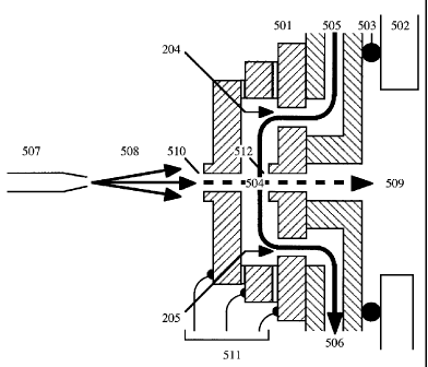
Figure 5 shows how the assembly 501 may be mounted on the wall of a vacuum
chamber 502
using an `0-ring' seal 503. In use, the inside of the vacuum chamber is
evacuated to low
pressure, while the outside is at atmospheric pressure. The central cavity 504
is maintained at
an intermediate pressure by passing a stream of a suitable drying gas such as
nitrogen from an
inlet 505 to an outlet 506 connected to a roughing pump. It will be
appreciated that the
pressure in the central cavity may be suitably controlled using different
combinations of inlet
pressure and roughing pump capacity and by the relative sizes of the openings
204 and 205.
The flux of ions is provided from a capillary 507 containing a liquid that is
(for example)
derived from a liquid chromatography system or capillary electrophoresis
system in the form
of analyte molecules dissolved in a solvent. The flux of ions is generated as
a spray 508 by
providing a suitable electric field near the capillary. In addition to the
desired analyte ions,
which it is desired to pass as an ion stream 509 into the vacuum chamber, the
spray typically
contains neutrals and droplets with a high concentration of solvent.
7
CA 02590762 2007-05-31
Ions and charged droplets in the spray may be concentrated into the inlet of
the assembly by
the first lens element carrying the proud feature 510, which is maintained at
a suitable
potential by one of the connections 511 provided on external surfaces of the
first, second or
third wafers. Entering the central chamber 504, the ion velocities may be
thermalised and the
spray may be desolvated by collision with the gas molecules contained therein.
The gas
stream may be heated to promote desolvation, for example by RF heating caused
by applying
an alternating voltage between two adjacent lens elements and causing an
alternating current
to flow through the silicon. Alternative mechanisms of achieving heating of
the stream may
include a heating prior to entry into the interface device where for example
it is considered
undesirable to actively heat the materials of the interface device.
Ions may be further concentrated at the outlet of the assembly by the second
lens element and
the third element carrying the proud feature 512, which are also maintained at
suitable
potentials by the remaining connections 511.
It will be appreciated that more complex assemblies of a similar type may be
constructed. For
example, Figure 6 shows the combination of two etched BSOI substrates 601 and
602 with a
third single-layer substrate 603 to form a serial array in the form of a 5-
layer assembly 604.
Here the ion stream 605 must pass now through two cavities 606 and 607 at
intermediate and
successively reducing pressures. The gas therein is again provided by a gas
stream taken from
an inlet 608 to an outlet 609 by a system of buried, etched channels that pass
through the two
chambers 606 and 607. The relative pressure in the two chambers 606 and 607
may be
controlled, by varying the dimensions of the connecting orifices 610 and 611.
Such a system
corresponds to a two-stage vacuum interface, and it will be apparent that
interfaces with even
more stages may be constructed by stacking additional layers.
Heretofore an interface component in accordance with the teaching of the
invention has been
described with reference to an exemplary arrangement where a laminated silicon
interface is
provided to allow transport of an ion stream between atmospheric pressure and
vacuum
through a pair of orifices sandwiching a chamber held at intermediate
pressure.
8
CA 02590762 2007-05-31
As was described above, such an interface may be constructed from a pair of
silicon
substrates. Where so constructed, the outer substrate may be fabricated from a
silicon-oxide-
silicon bilayer, while the inner substrate may be provided in the form of a
silicon monolayer.
As was described wither reference to Figures 3 and 4, these two substrates may
then be
hermetically bonded together, and then bonded to a stainless steel vacuum
flange containing a
gas channel. As was illustrated with reference to Figure 5, the completed
assembly may then
be used to to couple an ion stream from a spraying device into a vacuum
system. The
preferential transmission of ions (as opposed to neutrals) is encouraged in
such an
arrangement by a judicious application of appropriate voltages to the three
silicon layers. In
the exemplary illustrative embodiments, the outer and inner layers contained
field-
concentrating features, while the inner layer contained a chamber. The three
elements acted
together to focus an ion stream emerging from the outer orifice onto the inner
orifice.
Such an arrangement may be successfully used to effect ion transmission and to
obtain mass
spectra from the resulting ion stream. The arrangement and performance may
however benefit
from one or more modifications, the specifics of which will be described as
follows.
As will be appreciated from the teaching of the invention most features of the
interface
component may be fabricated using standard patterning, etching and
metallisation processes,
as will be familiar to those skilled in the art.
Figure 7 shows an alternative arrangement for providing an interface component
according to
an aspect or embodiment of the invention. It will be recalled from the
discussion of Figure 3
that the option of bonding the two surfaces 303, 304 together by means of a
solder joint was
expressed. While such an arrangement does provide the necessary coupling
between the two
surfaces it does present a possibility of a short circuit being formed by the
solder across the
isolating layer of oxide 104 between the lower substrate 302 and the lower
layer of the upper
substrate 301- this possibility arising from their very close proximity to one
another. If such a
short circuit is effected then it is difficult to apply a different voltage to
the two layers.
The arrangement of Figure 7 obviates the need to co-locate a soldered joint
with an insulating
layer. In the arrangement of Figure 7, an upper substrate 701 is configured to
contain a
9
CA 02590762 2007-05-31
laterally isolated electrode 702, which is suspended inside a perimeter of
silicon. The surfaces
703 of the upper substrate and the flange 705 may be coated with a conducting
material which
is desirably un-reactive and non-oxide forming- gold being a suitable example.
Surfaces 704
of the lower substrate 706 may be solder coated.
To assemble such an arrangement, each of the two substrates 701, 706 may be
stacked on the
flange 705 and then secured by a melting of the solder 704, as shown in Figure
7b. Although
a short circuit is now always created between the lower substrate 706 and a
lower contacting
layer 707 of the upper substrate 701, its existence is immaterial, as the
suspended electrode
702 is isolated from these contacted surfaces. By providing an access hole 708
through the
upper substrate 701, a different voltage can now be applied to the suspended
electrode 702
via a bond wire 709 passing through the access hole. The utilisation of a
suspended electrode
also allows the distances between the electrode and the lower substrate to be
reduced at the
point of the ion path 713.
In the arrangement of Figure 1, a channel 110 was described as passing through
a central
chamber 109, to allow the passage of gas during pumping. While such an
arrangement
suffices to provide for the passage of gas, it is desirable to have a large
cross-section area for
this passage in order to obtain effective pumping of the intermediate chamber.
In the
arrangement of Figure 1, this cross section area is difficult to achieve
without effecting a
removal of most of the walls of the chamber 109, which could affect the ion
focusing
capabilities.
In the arrangement of Figure 7, it will be noted that the lower substrate 706
is provided with a
pair of recess features 711 which are co-located with the suspended electrodes
702 of the
upper substrate. The provision of the recess features is advantageous in that
it ensures that the
suspended electrode does not come into contact with the lower substrate 706
when the two
substrates are brought into intimate contact with one another- Figure 7b. It
will be noted that
the recess features 711 are dimensioned sufficiently to avoid electrical
contact between the
lower substrate and the suspended electrode. A secondary or additional benefit
is provided in
that the recess features 711 provide a gas flow path 712. This path can be
advantageously
used either to remove neutrals or to admit a drying gas, without the need to
pass a channel
CA 02590762 2013-01-31
across the layer containing the central chamber. Consequently, the channel may
be omitted
entirely from this layer. This arrangement may provide more effective ion
focussing.
In the arrangement of Figure 7, field concentrating features 714, 715 in the
upper and lower
substrates are essentially raised capillaries. In a further modification to
the exemplary
embodiments heretofore described it is possible to provide improved field
concentration and
improved momentum separation of ions and neutrals if the outer walls 801, 802
of these
features are sloped at around 600, as shown in Figure 8a.
It is generally difficult to construct features with well-controlled,
continually varying slopes
using standard microfabrication processes such as dry etching. However,
features with
approximately correct slopes may be constructed by crystal plane etching. In
silicon, the (111)
planes can be shown to etch much more slowly than all other planes in certain
wet etchants,
for example potassium hydroxide. These planes lie at an angle cos-1(1/-0) =
54.730 to the
surface of a (100) oriented wafer, and provide a natural boundary to etched
features. The
(211) planes also etch relatively slowly.
A proud feature 800 whose surfaces consist of four (111) planes and four (211)
planes as
shown in Figure 8b may be therefore constructed by etching a (100) wafer
carrying a surface
mask of etch resistant material such as silicon dioxide, which is patterned to
form a square.
Such a feature may therefore provide improved field concentration and momentum
separation, and could be used independently of an interface component for
coupling an ion
source to a vacuum system- as will be appreciated by those skilled in the art
could the
suspended electrode of Figure 7.
It will also be appreciated that there is considerable scope for variations in
layout and
dimension in the arrangements above. For example, it is not necessary for the
ion path to be
co-linear from input to output, and reduced contamination of the vacuum system
may follow
from adopting a staggered ion path so that no line of sight exists. Similarly,
it is not necessary
for both of the orifices to be circular in geometry, and reduced contamination
may again arise
from (for example) the combination of a first circular orifice with a second
circular annular
orifice.
11
CA 02590762 2007-05-31
It will also be appreciated that the silicon parts may be fabricated in a
batch process so that
the assembly may be provided as a low-cost disposable element. Finally, it
will be
appreciated that because the entire vacuum interface is now reduced in size, a
plurality of
similar elements may be constructed as an array on a common substrate. The
array may then
provide interfaces for a plurality of electrospray capillaries.
It will be understood that what has been described herein are exemplary
embodiments of
microengineered interface components which are provided to illustrate the
teaching of the
invention yet are not to be construed in any way limiting except as may be
deemed necessary
in the light of the appended claims. Whereas the invention has been described
with reference
to a specific number of layers it will be understood that any stack
arrangement comprising a
plurality of individually patterned semiconducting layers with adjacent layers
being separated
from one another by insulating layers, and orifice defined within the layers
defining a conduit
through the stack should be considered as falling within the scope of the
claimed invention.
Within the context of the present invention the term microengineered or
microengineering is
intended to define the fabrication of three dimensional structures and devices
with dimensions
in the order of microns. It combines the technologies of microelectronics and
micromachining. Microelectronics allows the fabrication of integrated circuits
from silicon
wafers whereas micromachining is the production of three-dimensional
structures, primarily
from silicon wafers. This may be achieved by removal of material from the
wafer or addition
of material on or in the wafer. The attractions of microengineering may be
summarised as
batch fabrication of devices leading to reduced production costs,
miniaturisation resulting in
materials savings, miniaturisation resulting in faster response times and
reduced device
invasiveness. Wide varieties of techniques exist for the microengineering of
wafers, and will
be well known to the person skilled in the art. The techniques may be divided
into those
related to the removal of material and those pertaining to the deposition or
addition of
material to the wafer. Examples of the former include:
= Wet chemical etching (anisotropic and isotropic)
= Electrochemical or photo assisted electrochemical etching
= Dry plasma or reactive ion etching
12
CA 02590762 2007-05-31
= Ion beam milling
= Laser machining
= Eximer laser machining
Whereas examples of the latter include:
= Evaporation
= Thick film deposition
= Sputtering
= Electroplating
= Electroforming
= Moulding
= Chemical vapour deposition (CVD)
= Epitaxy
These techniques can be combined with wafer bonding to produce complex three-
dimensional, examples of which are the interface devices provided by
illustrative
embodiments of the present invention.
While the device of the exemplary embodiments of invention has been described
as an
interface component it will be appreciated that such a device could be
provided either
separate to or integral with the other components to which it provides an
interface between.
By using an interface component it is possible to remove impurities or other
unwanted
components of the emitted spray material from the capillary needle
conventionally used with
mass spectrometer system.
It will be further understood that whereas the present invention has been
described with
reference to an exemplary application, that of interfacing an ionization
source-specifically an
electrospray ionization source- with a mass spectrometry system, that
interface components
according to the teaching of the invention could be used in any application
that requires a
coupling of an ion beam from an ionization source provided at a first pressure
to another
device that is provided at a second pressure. Typically this second pressure
will be lower than
13
CA 02590762 2007-05-31
the first pressure but it is not intended to limit the present invention in
any way except as may
be deemed necessary in the light of the appended claims.
Where the words "upper", "lower", "top", bottom, "interior", "exterior" and
the like have
been used, it will be understood that these are used to convey the mutual
arrangement of the
layers relative to one another and are not to be interpreted as limiting the
invention to such a
configuration where for example a surface designated a top surface is not
above a surface
designated a lower surface.
Furthermore, the words comprises/comprising when used in this specification
are to specify
the presence of stated features, integers, steps or components but does not
preclude the
presence or addition of one or more other features, integers ,steps,
components or groups
thereof.
References
Whitehouse C.M., Dreyer R.N., Yamashita M., Fenn J.B. "Electrospray interface
for liquid
chromatographs and mass spectrometers" Anal. Chem. 57, 675-679 (1985)
Labowsky M.J., Fenn J.B. "Method and apparatus for the mass spectrometric
analysis of
solutions" US 4,531,056 July 23 (1985)
Valaskovic G.A., McLaffert F.W. "Electrospray ionization source and method of
using the
same" US 5,788,166 Aug 4 (1998)
Bruins A.P., Covey T.C., Henion J.D. "Ion spray interface for combined liquid
chromatography/ atmospheric pressure ionization mass spectrometry" Anal. Chem.
59,
2642-2646 (1987)
14
CA 02590762 2007-05-31
Duffin K.L., Wachs T., Henion J.D. "Atmospheric-pressure ion-sampling system
for liquid-
chromatography mass-spectrometry analyses on a benchtop mass-spectrometer"
Anal.
Chem. 64, 61-68 (1992)
Ryhage E.R. "Molecule separator" US 3,803,811 April 16 (1974)
Mordehai A. "Skimmer for mass spectrometry" US 6,703,610 Mar 9 (2004)
Schneider B., Covey T.R. "Atmospheric pressure charged particle discriminator
for mass
spectrometry" US 7,098,452B2 Aug 29 (2006)
Mylchreest I., Hail M.E. "Electrospray ion source with reduced neutral noise
and method"
USRE35413E Dec 31 (1996)
Apffel J.A., Werlich M.H., Bertsch J.L., Goodley P.C., Henry K.D. "Orthogonal
ion sampling
for apci mass spectrometry" US 6,797,946 Sept 28 (2004)
Milchreest I., Hail M.E., Heron J.R. "Method and apparatus for focusing ions
in viscous flow
jet expansion region of an electrospray apparatus" US5157260 Oct 20 (1992)
Tomany M.J., Jarrell J.A. "Housing for converting an electrospray to an ion
stream" US
5,304,798 April 19 (1994)
Sheehan E.W., Willoughby R.C. "Laminated lens for focusing ions from
atmospheric
pressure" US6818889 B1 Nov 16 (2004)