Note: Descriptions are shown in the official language in which they were submitted.
CA 02591349 2007-06-07
WO 2006/068974 PCT/US2005/045750
ELECTRICAL CONNECTOR WITH CROSSTALK
COMPENSATION
[0001] The invention relates generally to electrical connectors, and
more particularly, to a modular connector with compensation for crosstalk
among
multiple signal paths through the connector.
[0002] In electrical systems, there is increasing concern for
preserving signal integrity as signal speed and bandwidth increase. One source
of
signal degradation is crosstalk between multiple signal paths. In the case of
an
electrical connector carrying multiple signals, crosstalk occurs when signals
conducted over a first signal path are partly transferred by inductive or
capacitive
coupling into a second signal path. The transferred signals produce crosstalk
in the
second path that degrades the signal routed over the second path.
[0003] For example, a typical industry standard type RJ-45
communication connector includes four pairs of conductors defining four
different
signal paths. In conventional RJ-45 plug and jack connectors, all four pairs
of
conductors extend closely parallel to one another over a length of the
connector body.
Thus, the problem is that signal crosstalk may be induced between and among
different pairs of connector conductors. The amplitude of the crosstalk, or
the degree
of signal degradation, generally increases as the frequency increases.
[0004] In the case of RJ-45 connectors, the plug design is controlled
by industry standards which require it to contain a substantial amount of
crosstalk.
Therefore, efforts to counteract crosstalk are typically applied to the mating
jack. In
one approach, terminal contacts in the jack are formed with free ends that are
deflected to contact a compensation coupling contact when a plug is mated with
the
jack. See, for example, U.S. Patent No. 6,350,158. In general, the
effectiveness of
these measures is influenced by the proximity of the corrective measure to the
main
source of the crosstalk, e.g., the mating plug.
[0005] The solution to the problem is provided by an electrical jack
as disclosed herein that suppresses or compensates for crosstalk, and ideally,
the
-1-
CA 02591349 2007-06-07
WO 2006/068974 PCT/US2005/045750
crosstalk compensation is introduced as close as possible to the source of the
crosstalk. The electrical jack includes a housing having a mating end
configured to
receive a mating plug. A plurality of signal contacts are arranged in
differential pairs,
and each of the signal contacts carries a signal from or to a plug contact in
the mating
plug. The electrical jack includes a plurality of compensation contacts,
wherein each
compensation contact engages a respective plug contact in the mating plug
independent of the signal contact, and the compensation contacts provide
crosstalk
compensation.
[0006] The invention will now be described by way of example wit
reference to the accompanying drawings in which:
[0007] Figure 1 is a perspective view of a connector having a jack
formed in accordance with an exemplary embodiment of the present invention.
[0008] Figure 2 is a perspective view of the plug shown in Figure 1
mated with a jack insert formed in accordance with the present invention.
[0009] Figure 3 is a perspective view of the jack insert shown in
Figure 2.
[0010] Figure 4 is a side view of the jack insert shown in Figures 2
and 3 with mated plug contacts.
[0011] Figure 5 is a perspective view of a jack insert with
compensation contacts formed in accordance with an alternative embodiment of
the
present invention.
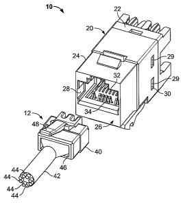
[0012] Figure 1 is a perspective view of a connector having a jack 10
formed in accordance with an exemplary embodiment of the present invention,
and a
plug 12 that is configured to mate with the jack 10. The jack 10, in an
exemplary
embodiment, is a modular jack. The jack 10 may be mounted on a wall or panel,
or,
alternatively, may be mounted in an electrical device or apparatus having a
communications port through which the device may communicate with other
external
networked devices. The jack 10 will be described in terms of an RJ-45 jack.
-2-
CA 02591349 2007-06-07
WO 2006/068974 PCT/US2005/045750
However, it is to be understood that the benefits described herein are also
applicable
to other connectors in alternative embodiments. The following description is
therefore provided for illustrative purposes only and is but one potential
application of
the inventive concepts herein.
[0013] The jack 10 includes a housing 20 that has a base portion 22
and a shell 24. The shell 24 includes a mating face 26 that defines an opening
28 that
is configured to receive the mating plug 12. Latch members 29 on the base
portion 22
are received in slots 30 in the shell 24 to retain the shell to the base
portion 22 with
snap fit engagement. The housing 20 includes a plurality of signal contacts 32
and a
plurality of compensation contacts 34 in an interior of the shell 24. The
compensation
contacts 34 may or may not be equal in number to the number of signal contacts
32.
[0014] The plug 12 includes a plug housing 40 that receives a cable
42 that includes a number of signal wires 44 that are arranged in differential
pairs.
Each signal wire 44 is attached to a plug contact 50 (Figure 2) within the
plug housing
40. The cable 42 extends from a cable receiving end 46 of the housing 40. A
lever 48
locks the plug 12 into the jack 10 with a snap fit. A plurality of plug
contacts 50
(Figure 2) engage the signal contacts 32 and the compensation contacts 34 when
the
plug 12 is mated to the jack 10.
[0015] Figure 2 is a perspective view of the plug 12 mated with a
jack insert 52 formed in accordance witll one embodiment of the present
invention.
The plug 12 houses plug contacts 50 that are attached to the signal wires in
the cable
42. The plug contacts 50 are held in the plug housing 40. The plug contacts 50
are
shown in mating engagement with the signal contacts 32 and the compensation
contacts 34. A typical RJ-45 connector includes eight plug contacts 50.
However, in
some embodiments, some plug contacts 50 may not be present, or if present, may
not
be used.
[0016] In an exemplary embodiment, the jack insert 52 is contained
within the jack housing 20. The jack insert 52 includes a first circuit board
60 and a
second circuit board 62. The signal contacts 32 are mounted in the first
circuit board
60. The signal contacts 32 are arranged in differential pairs. Traces in the
first circuit
-3-
CA 02591349 2007-06-07
WO 2006/068974 PCT/US2005/045750
board 60 electrically connect each signal contact 32 to a respective aperture
64 that is
configured to receive an output terminal (not shown) that electrically
connects the
signal contact 32 to an output wire (not shown) that carries one of the
differential
signals from or to the plug 12 when the plug 12 is mated to the jack 10.
[0017] The second circuit board 62 includes an upper surface 70, a
lower surface 72, an inward end 74 proximate the first circuit board 60, and
an
outward end 76 proximate the mating face 26 of the jack 10 (Figure 1). The
second
circuit board 62 is housed in a channel (not shown) in the jack shell 24
(Figure 1). In
one embodiment, the compensation contacts 34 are mounted over the outward end
of
the second circuit board 62. In other embodiments, the compensation contacts
34 may
take other forms. For instance, the compensation contacts 34 may be mounted in
and
upwardly extend from the upper surface 70 of the second circuit board 62. In
one
embodiment, one or more compensation elements (not shown) may be mounted on
the
second circuit board 62. Some or all of the compensation contacts 34 will
electrically
connect to one or more compensation elements (not shown) located on the second
circuit board 62. The compensation elements are selected to provide a desired
noise
compensation to the mating plug contacts. '
[0018] More specifically, the compensation elements are selected to
provide a desired crosstalk compensation to counteract crosstalk at the plug
contacts
in the mating plug 12 through direct contact of the compensation contacts 34
with the
plug contacts 50. From the perspective of the jack 10, the plug contacts 50
and the
portion of the wires 44 contained within the plug housing 40 (Figure 1) are
considered
to be a noise source, or more specifically, a source of crosstalk. Thus, in
applying
compensation directly to the plug contacts 50, the crosstalk compensation is
applied to
the source of the crosstalk.
[0019] In one embodiment, the compensation elements (not shown)
include a conductive element that provides a reactance that is configured to
counteract
the crosstalk that is seen in the plug 12. In an exemplary embodiment, the
reactance
primarily includes a capacitance. The compensation elements may be formed
using
techniques well known in the art for such purposes. For example, two or more
-4-
CA 02591349 2007-06-07
WO 2006/068974 PCT/US2005/045750
compensation contacts 34 may be placed in close proximity to each other so as
to
create the reactance to counteract the crosstalk. Another method may include
placing
conductors on the circuit board 62 in close proximity to one another, such as
interlaced or aligned copper pours. A third method may include placing
discrete chips
such as a capacitor on the circuit board 62. Still another method may include
placing
conductive plates in proximity with one another (see Figure 5). The
compensation
elements may also include other circuit components that create a coupling to
counteract the crosstalk within the plug 12.
[0020] Figure 3 illustrates a perspective view of the jack insert 52 in
greater detail. Figure 4 illustrates a side view of the jack insert 52 with
mated plug
contacts 50. The compensation contacts 34 are physically aligned with the
signal
contacts 32 within the jack 10, however, the number of compensation contacts
34 may
or may not correspond to the number of signal contacts 32. When the plug 12 is
mated with the jack 10, each of the plug contacts 50 is engaged by one of the
signal
contacts 32 and one of the compensation contacts 34 within the jack 10 when
both the
signal contact 32 and the compensation contact 34 are present. In one
embodiment of
the invention, the signal contacts 32 and the compensation contacts 34 are
oriented
within the jack 10 such that as the plug 12 is mated with the jack 10, the
plug contacts
50 engage the compensation contacts 34 prior to engaging the signal contacts
32. In
otlier embodiments, the compensation contacts 34 can be placed such that the
plug
contacts 50 engage the signal contacts 32 prior to engaging the compensation
contacts
34. The compensation contacts 34, which are non-current carrying contacts, and
the
signal contacts 32 engage the plug contacts 50 independently of one another
regardless of the order of engagement of the signal contacts 32 and the
compensation
contacts 34 with the plug contacts 50. The signal contacts 32 and the
compensation
contacts 34 are not electrically connected to one another other than through
the plug
contacts 50.
[0021] Each signal contact 32 includes an engagement end 78 that
engages the plug contact 50 when the plug 12 (Figure 2) is mated to the jack
10
(Figure 1). Mounting ends 80 of the signal contacts 32 are received in the
first circuit
-5-
CA 02591349 2007-06-07
WO 2006/068974 PCT/US2005/045750
board 60 and are electrically connected to traces (not shown) in the first
circuit board
60.
[0022] In an exemplary embodiment, each compensation contact 34
includes an attachment loop 82 that loops over the outward end 76 of the
circuit board
62. Bend portions 84 cooperate with the loop 82 so that the compensation
contact 34
grasps the outward end 76 of the second circuit board 62 to frictionally
engage the
upper and lower surfaces 70 and 72 of the second circuit board 62. A contact
arch 86
mates with the plug contact 50 when the plug 12 is mated with the jack 10. The
compensation contacts 34 may be electrically connected to the second circuit
board 62
through contact pads 88. In one embodiment, the contact pads 88 are placed on
the
upper surface 70 of the second circuit board 62. In other embodiments, the
contact
pads may be placed on either or both of the upper and lower surfaces, 70 and
72
respectively, of the second circuit board 62. In alternative embodiments, the
compensation contacts 34 may take other forms. For instance, the compensation
contacts may include mounting ends that are mounted in the second circuit
board 62
and curved contact ends as opposed to the contact arches 86.
[0023] The second circuit board 62 includes compensation elements
(not sliown) that are electrically connected to some or all of the
compensation contacts
34. The compensation elements are each selected and configured to provide , a
predetermined amount of crosstalk compensation to the signal at the mating
plug
contacts 50. The crosstalk compensation is applied directly to the plug
contacts 50 of
the mating plug 12. The compensation contacts 34 are themselves non-current
carrying contacts such that the crosstalk compensation is applied to the
signal at the
plug contacts 50 to effectively eliminate any electrical delay in the
application of
compensation to the plug contacts 50.
[0024] Figure 5 is a perspective view of a jack insert 90 formed in
accordance with an alternative embodiment of the present invention. The jack
insert
90 includes the first circuit board 60, but is without a second circuit board.
The jack
insert 90 includes alternative compensation contacts 92. The compensation
contacts
92 are mounted in the housing shell 24 (Figure 1) proximate the mating face
26. The
-6-
CA 02591349 2007-06-07
WO 2006/068974 PCT/US2005/045750
jack insert 90 also includes signal contacts 32. In Figure 5, plug contacts 50
are
shown as they would engage the signal contacts 32 and compensation contacts 92
when the plug 12 is mated with the jack 10. The compensation contacts 92 and
signal
contacts- 32 are oriented so that both engage the plug contacts 50
independently of
each other. In the illustrated embodiment, each of the compensation contacts
92
includes a plate 94 that is electrically connected to the compensation contact
92. In
other embodiments, one or more of the compensation contacts 92 may not include
a
plate 94. The plates 94 are sized and configured in proximity to each other so
that
their electromagnetic fields will interact creating compensation elements. The
compensation elements provide a predetermined amount of noise, or more
specifically, crosstalk compensation.
[0025] In the einbodiment shown in Figure 5, the compensation
contacts 92 are cane shaped and are oriented such that the compensation
contacts 92
are alternately outwardly facing and inwardly facing to provide space for the
plates 94.
The alternating orientation of the compensation contacts 92 may also provide
for
flexibility in varying the electromagnetic coupling between the various plates
94. As
previously described, the crosstalk compensation is applied directly to the
plug contact
50. The compensation contacts 92 are non-current carrying contacts and
therefore the
crosstalk compensation is effectively applied to the plug contacts 50 without
any
electrical delay.
[0026] The embodiments thus described provide a modular jack 10
that compensates for crosstalk in the signals from a mating plug 12. The jack
10
applies the crosstalk compensation at the source of the crosstalk. The jack 10
includes
a signal contact 32 and a separate compensation contact 34, 92 botll of which
engage
the plug contact 50 of the mating plug 12. Crosstalk compensation is applied
directly
to the plug contact 50 of the plug 12. The compensation contact 34, 92 is a
non-
current carrying contact. In this manner compensation is effectively applied
to the
plug contact 50 without any electrical delay.
-7-