Note: Descriptions are shown in the official language in which they were submitted.
CA 02591651 2007-05-14
1
TITLE OF THE INVENTION:
Shadow Sculpted Thin Films
NAME(S) OF INVENTOR(S):
Kevin John Robbie
Michael Julian Brett
FIELD OF THE INVENTION
This invention relates to the deposition of
shadow sculpted thin films on substrates.
CLAIM TO COPYRIGHT
A portion of the disclosure of this patent
document contains material which is subject to copyright
protection. The copyright owner has no objection to the
facsimile reproduction by anyone of the patent document, as
it appears in the Patent Office patent file or records, but
otherwise reserves all copyright rights whatsoever.
BACKGROUND OF THE INVENTION
In the art of growing thin films, it is known to
expose a substrate to an oblique incident vapor flux in
conditions of limited adatom diffusion and thus grow a
columnar microstructure on the substrate.
The optical properties of the resulting
microstructure are dependent in part on the material used,
CA 02591651 2007-05-14
2
the porosity of the microstructure and the orientation of
the columns of the thin film.
Hamaguchi et al, United States patent no.
4,874,664, describe lateral shifting or rotation of the
position of the substrate in relation to the vapor flux to
create uniform film growth and film layers that have
columns with different orientations in the different
layers. In Hamaguchi et al, the entire substrate is rotated
in between periods of exposure of the substrate to vapor
flux, or the substrate is laterally shifted during exposure
to vapor flux.
The angle of the incident vapor flux in the prior
art tends to be in the range from near 0 to 70 where the
angle is measured between the vapor arrival line and the
substrate normal, which may be referred to as the polar
angle. Where the polar angle is zero, the deposited film is
a uniform layer, and does not generate the columnar
microstructure. For stationary substrates, results have
been published for polar angles reaching close to 90 . The
angle of growth of the columns is related in a way poorly
understood to the angle of incidence of the vapor flux, but
is always observed to be smaller, as measured from the
substrate normal, than the angle of incidence.
A paper of Azzam, "Chiral thin solid films",
Appl. Phys. Lett. 61 (26) 28 December 1992, has proposed
rotation of the substrate while it is exposed to the
oblique incident vapor flux to generate a helical
microstructure having helicoidal bianisotropic properties.
The proposed rotation of the substrate is about an axis
perpendicular to the surface of the substrate, which is
referred to in this patent document as rotation about the
azimuth, or variation of the azimuthal angle. No particular
polar angle is specified, though a figure shows an angle of
less than 60 . The inventors have attempted to grow
CA 02591651 2007-05-14
3
microfilm structures by rotation of the substrate in the
presence of a vapor flux incident at a polar angle of about
60 and 70 . However, the resulting structure does not show
well defined structures.
The paper of Assam is a theoretical paper and
fails to provide directions on how to carry out the method
in practice. In addition, the patent of Hamaguchi et al
provides only one particular microstructure, with limited
variation of the columnar growth.
SUMMARY OF THE INVENTION
This invention seeks to overcome some of the
limitations of the prior art and provide a film forming
system method and apparatus that allows for the growth of
complex microstructures with predetermined patterns of
growth. In addition, porosity and optical properties of the
shadow sculpted thin film are enhanced by expanding the
range of incidence angles of the vapor flux. Further, a
method is provided for capping a porous columnar
microstructure with a dense film.
Further, the inventors have found to their
surprise that rotation of the substrate while it is exposed
to an oblique incident vapor flux at polar angles greater
than about 80 produces well defined microstructures.
Therefore, in accordance with one aspect of the
invention, there is provided a method of sculpting vapor
deposited thin films, the method comprising the steps of:
initially exposing a surface of a substrate to a
vapor flux at an oblique incident angle to grow a columnar
thin film; and
subsequently, and while continuing to expose the
surface to vapor flux, rotating the substrate about an axis
parallel to the plane of the substrate.
CA 02591651 2007-05-14
4
In a further aspect of the invention, there
includes the step of, while initially exposing the
substrate to vapor flux, moving the substrate to alter the
direction of growth of the columns, as for example by
rotating the substrate about a normal to the surface of the
substrate to create a helical film growth. The substrate
may then be rotated about an axis parallel to the plane of
the substrate to form a cap for the helical thin film
growth. In a further aspect,. a cap may be formed by
exposing the substrate to a vapor flux in conditions of
high diffusion length, such that a dense uniform mass is
obtained, such as by heating the substrate to nearly the
melting point of the material forming the vapor flux.
In a further aspect of the invention, tailored
film growths may be obtained by (a) establishing, in a
computer, a desired pattern of thin film growth; (b) while
exposing a surface of a substrate to a vapor flux at an
oblique incident angle, changing the orientation of the
surface in relation to the angle of incidence of the vapor
flux; (c) providing control signals to the computer
indicative of thin film growth on the substrate; and (d)
automatically controlling the rate of change of the
orientation of the surface in response to the control
signals to grow the thin film according to the desired
pattern.
In a still further aspect of the invention, there
is provided a method of sculpting vapor deposited thin
films, the method comprising the steps of exposing a
surface of a substrate to a vapor flux at an oblique
incident angle; and, at the same time, rotating the
substrate about a normal to the surface while maintaining
the oblique angle at greater than 80 .
In a still further aspect of the invention, there
is provided an apparatus for growing thin films on a
CA 02591651 2007-05-14
substrate having a surface, the apparatus comprising a
vacuum chamber; a vapor source; a first motor disposed in
the vacuum chamber above the vapor source, and having a
first rotational axis, the first motor having a shaft and
5 means for mounting a substrate on the shaft such that the
first rotational axis is normal to the surface of the
substrate; a driver for the first motor; a deposition rate
monitor having output signals indicative of thin film
growth on a substrate exposed to vapor flux from the vapor
source; and a controller responsive to the output signals
for instructing the drivers to cause the first motor to
rotate according to a desired pattern. According to a
second aspect of the apparatus of the invention, there is
also provided a second motor disposed in the vacuum chamber
above the vapor source, and having a second rotational axis
at about 90 to the first rotational axis. The first motor
is mounted on the shaft of the second motor such that the
second rotational axis is parallel to the surface of the
substrate. A driver, which may be the same driver as for
the first motor, is also provided for the second motor. The
controller is also responsive to the output signals to
cause the second motor to rotate according to a second
desired pattern.
In a further aspect of the invention, a thin film
microstructure is provided wherein vapor deposited material
extends in distinct helical columns from a substrate. The
columns may be capped, and may be supplied with electrodes
to form a delay line or a variable wavelength optical
filter.
In a still further aspect of the invention, the
substrate may be provided with small mounds spaced
sufficiently close together that growths are confined to
grow on the mounds and not between them. In this way, the
CA 02591651 2007-05-14
6
spacing of the helical growths can be determined in advance
of deposition.
These and other aspects of the invention are
described in the detailed description of the invention and
claimed in the claims that follow.
BRIEF DESCRIPTION OF THE DRAWINGS
There will now be described preferred embodiments
of the invention, with reference to the drawings, by way of
illustration, in which like numerals denote like elements
and in which:
Fig. 1 is a schematic illustrating prior art
understanding of how shadow sculpting forms columnar film
microstructures;
Fig. 2 is a schematic showing apparatus according
to one aspect of the invention for depositing a thin film
on a substrate using a vapor flux, with an exemplary
substrate shown in side view, thereby illustrating how
polar angle variation alters the incidence of the vapor
flux;
Fig. 3 shows the apparatus of Fig. 2 with the
substrate in plan view, thereby illustrating rotation of
the substrate about a normal to the plane of the substrate;
Fig. 4 shows control elements for use with the
apparatus of Figs. 2 and 3;
Fig. 4A shows an arrangement of the azimuthal and
polar angle control motors;
Figs. 5A, 5B, 5C and 5D are graphs illustrating
polar (Figs. 5A, 5B and 5C) and azimuthal (Fig. 5D) angle
variations;
Fig. 6 is a scanning electron micrograph showing
helical columns of MgF2;
Fig. 7A is a side view of a thin film with
helical growths deposited on a substrate;
CA 02591651 2007-05-14
7
Fig. 7B is a side view of a thin film as in Fig.
7A with a cap, showing electrodes schematically (the
electrodes are not necessarily to scale, since in practice
each electrode could cover thousands of helixes);
Fig. 7C is a side view of the thin film of Fig.
7B with electrode plates bounding the structure;
Fig. 8 is a side view of a substrate with mounds
for pre-determining the location of helical growths; and
Fig. 9 is a plan view of a substrate with mounds
showing one particular pattern of mounds.
DETAILED DESCRIPTION OF PREFERRED EMBODIMENTS
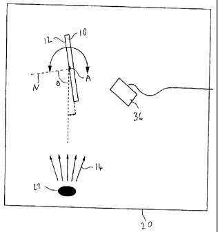
Fig. 1 illustrates the physical process
underlying growth of a slanted columnar film microstructure
as is known in the prior art. A substrate 10, for example
a silicon wafer, has a surface 12 with normal N and is
exposed to an oblique incident vapor flux 14 whose angle of
incidence, defined in relation to the normal N, is 8. As
atoms in the vapor flux 14 are deposited onto the substrate
10, film growth areas atoms shadow adjacent regions 16,
preventing deposition of vapor in these regions. Atoms in
the vapor flux 14 continue to be deposited in regions that
are not shadowed, thus forming columns 18. Atoms diffuse
adatomically across the tops of the columns as shown at 19.
Slanted columnar microstructures will grow if the angle 0
is sufficiently large to create the shadowing effect, and
there is limited adatom diffusion 19, such that adatom
diffusion does not fill in the gaps between columns. In
practice, angle 0 need only be slightly above 01 to form
reasonably defined columns and columnar structures will
form in many substances at 0 = 0 , though they may be hard
to discern under conditions such that the films have high
atom diffusion lengths, for example due to high
temperatures or materials with low melting points. The
CA 02591651 2007-05-14
8
angle R of the axis of the columns 18 to the normal N of
the substrate is less than 0. The actual relationship
between 0 and 0 is poorly understood, but approximations of
the relationship are known in the art.
"Oblique" as used in this patent document in
relation to an angle means sufficiently departing from 0
that atomic shadowing has an effect on the growth of
columnar microstructures. The substrate may be any solid
material on which a vapor may be deposited, and will depend
on the application. Silicon substrates will be commonly
used. The material to be deposited may be any material for
which conditions are achievable to support vapor generation
and deposition of the vaporized material on the substrate.
In some cases, this may require cooling or heating of the
substrate. To assist in bonding one vaporized material to
another, an intervening layer may be first deposited, as
for example using a chromium intermediate layer to bond
gold to amorphous silicon dioxide (glass). The processes
described here should be carried out in conditions in which
the vapor flux arrives at the substrate in approximately a
straight line. For this reason, it is preferred that the
process be carried out under conditions approximating a
vacuum, at less than 10-3 torr, for example at 10-6 torr. At
higher pressures, scattering from gas molecules tends to
prevent well defined structures from growing. In addition,
the material used should have a sticking co-efficient of at
least about 0.9 to enable the formation of distinct
structures.
Referring now to Figs. 2, 3 and 4, an apparatus
according to the invention is shown for growing a thin film
on a substrate 10 having a surface 12. A conventional vapor
source 22 is located within a vacuum chamber 20. A
conventional shutter (not shown) located above the vapor
source 22 is used to control whether or not the substrate
CA 02591651 2007-05-14
9
is exposed to vapor. Various conventional means (not
shown separately) for causing the vapor source 22 to emit
a vapor flux 14 may be used. A substrate 10 is supported in
the vacuum chamber 20 on a motor 24 (Fig. 4) disposed in
5 the vacuum chamber 20 above the vapor source 22. The motor
24 rotates the substrate about an axis A lying parallel to
and preferably in the plane defined by the surface 12 of
the substrate 10. Rotation of the substrate 10 about axis
A alters the polar angle, namely the angle of incidence 0
10 of the vapor flux 14. Motor 26, also disposed in the vacuum
chamber 20 above the vapor source 22, has a rotational axis
coinciding with the normal N of the substrate 10 and thus
alters the azimuthal angle. The polar angle and the
azimuthal angles are both measures of the orientation of
the surface of the substrate to the incident flux.
As shown in Fig. 4A, the substrate 10 is
preferably mounted on a disc 11 which is attached to motor
26. Various mounting arrangements of motor 24 and motor 26
may be used. For example, motor 26 may be mounted on a
frame 25, and the frame 25 may be mounted to rotate with
the drive shaft 27 of motor 24. Motor 24 itself may be
mounted by any of various conventional methods for mounting
motors within a vacuum chamber such as on a support 29.
Referring now to Fig. 4, motors 24 and 26 are
preferably conventional stepper motors driven by stepper
motor drive electronics 28 and controlled by computer
controller 30. The computer controller 30 includes a data
acquisition board 32 and a software based interface 34 such
as LabVIE" available from National Instruments. The data
acquisition board 32 receives signals indicative of thin
film growth on the substrate output from a deposition rate
monitor 36 of conventional construction located within the
vacuum chamber 20 in a location in which film growth on the
deposition rate monitor 36 is representative of film growth
CA 02591651 2007-09-24
on the substrate 10. In response to receiving the output
signals from the deposition rate monitor 36, the computer
controller 30 instructs the driver 28 to cause the motors 24
and 26 to rotate according to a desired pattern. As
5 described herein, the computer automatically controls the
rate of change of the orientation of the surface in response
to the output control signals to grow the thin film
according to the desired pattern. An exemplary software
program for programming the computer controller 30 may be
10 designed using LabVIEWT' software from the disclosure herein.
Start and stop signals for vapor deposition may be sent by
the computer to a drive for the shutter for starting vapor
deposition, or the shutter may be opened manually. Normally,
the motors are started before the shutter opens to initiate
deposition.
The software receives a deposition rate from the
deposition rate monitor. The actual thickness (T2) of the
film growing on the substrate is related to the thickness on
the deposition rate monitor by an empirically determined
scaling factor known as the tooling factor. The software
also knows the motor positions at the last time instant (Xfi
for motor 24, Xci for motor 26) and receives as input from
the operator, the number (N) of turns to be made by the
motor 26, the tooling factor (ratio of vertical film growth
rate to measured deposition rate), an initial deposition
rate estimate, an initial angle of incidence for the vapor
flux during sculpted film growth, motor rotation direction,
and various parameters that define the desired pattern of
growth for the film. The inputs to the computer establish
the desired pattern of film growth.
In the case of formation of helical film growths,
the pitch w of the helix must be specified, and in the case
of a capping layer for a film growth, both the cap thickness
CA 02591651 2007-09-24
11
(Tc) and number of turns (Nc) of the motor 24 must be
specified by the operator.
In an embodiment of the invention, the motors 24,
26 are step motors that rotate a fraction of a circle each
time instant, ti, ti+1, ti+2 etc. At any given time ti, the
computer has just updated the thickness of the film from the
deposition rate monitor 36 and changed the motor step rate
so that at ti+1, the motor 24, 26 will be at approximately
the desired position according to the desired pattern.
Between time instants ti and ti+1, the software calculates
what the thickness of the film growth will be at ti+2 and
calculates how fast the motors must rotate in order to give
the desired thickness at ti+2. At ti+2, the computer then
reads the new thickness from the deposition rate monitor as
well as the motor stepping rates, and adjusts the motor
stepping rate so that at ti+3 the film growth pattern will
be approximately as desired. The software continues in this
fashion until a stop signal is received, for example when
the film has reached a desired thickness.
Algorithms for controlling the motors 24, 26 in
the case of a helical film with a cap are illustrated
graphically in Figs. 5A-5D. For the motor 26, if helical
film growth has not reached the desired thickness, that is,
T2 is less than w*N, where * indicates multiplication
throughout this patent document, then Xc2 is 360 /w*T2, that
is, the substrate 10 is rotated to a position equal to 360
times the ratio of T2 to w. If T2 is greater than or equal
to w*N, that is, the helical film thickness has been
achieved, then during a capping process, Xc2 is
360*N+360*Nc/Tc*(T2-w*N), that is, Xc2 gradually increases
from 360*N to 360*(N+Nc) proportionally to the capping layer
thickness (T2-w*N). This rotation rate will typically be
faster than
CA 02591651 2007-05-14
12
the rotation rate during helical film growth, depending on
the choice of the factor Nc/Tc.
For the motor 24, if helical film growth has not
reached the desired thickness, the motor 24 does not change
position, hence polar or flux angle remains the same. If T2
is greater than or equal to w*N, then the new motor
position Xf2 equals the motor position at the last time
instant (Xfi) plus (90 - Xfi) times the ratio of the
difference of T2 from w*N to the thickness of the cap (that
is, Xfi = Xfi + (90 - Xfi)/Tc*(T2-w*N).
This last formula is represented graphically in
Fig. 5A. The polar angle (angle of incidence measured from
the normal) is kept constant over an initial period 40,
during which the surface of the substrate is exposed to
oblique incident vapor flux, and then rotated at a constant
angular rate to zero, while continuing to expose the
surface to vapor flux. Changing of the polar angle towards
zero produces a cap for the sculpted film growths. At zero
polar angle, the flux is normally incident. The algorithm
for controlling the azimuthal angle results in the
substrate rotating N times to achieve a helical film growth
of thickness T2 = w*N. During the capping process, the
substrate continues to rotate about the azimuth, typically,
but not necessarily, at a faster rate than during helical
film growth. During the period 40, the substrate 10 may be
(a) rotated about a normal to its surface to create helical
microstructures, (b) shifted 180 to form zig-zags, (c)
translated, (d) kept at a constant orientation to the vapor
source, or (e) otherwise rotated or translated to obtain a
desired growth pattern under the cap.
Alternatively, the cap for a film growth may be
created by exponentially decreasing polar angle as
illustrated in Fig. 5B. The algorithm for controlling the
polar angle is the same during helical film growth as for
CA 02591651 2007-05-14
13
the linear cap: the angle is the kept constant. During
capping, Xf2 is assigned the value Xfi plus (90-Xfi) times
e raised to the power of ((T2-w*N-Tc)/k), where k is the
exponential scale factor or time constant (for example,
800). Hence, the polar angle drops monotonically from near
900 to zero as T2 approaches the sum of w*N (the desired
thickness of the columnar layer) and Tc (the thickness of
the cap). As illustrated in Fig. 5B, polar angle is
constant during helical film growth (area 44) and
exponentially decreasing to zero in area 46. Rotation speed
of the substrate about its normal depends in part on the
deposition rate. For MgF2 at 85 angle of incidence, and a
pitch of about 50 nm, the speed is about 2 rpm. Typical
rotation speeds used in the process are about 0.2 to 3 rpm.
For higher deposition rates, higher speeds will be
possible, but the speed should not be so high so as to
destroy the distinct columnar features produced by the
invention.
Fig. 7A illustrates a thin film microstructure
produced by the process described here with rotation of the
substrate about a normal to the substrate. Vapor deposited
material extends in distinct (separate from one another)
helical columns 70 from the substrate 10. Fig. 7B
illustrates the same thin film with the distinct helical
columns 70 terminating distally from the substrate 10 in a
region of denser material forming a cap 74 for the helical
columns. The cap 74 may be produced by changing the angle
of incidence of the flux from 0 near 900 to zero (as in
Fig. 2) as described above (corresponding to rotation about
an axis parallel to the substrate surface), or, it is
believed on reasonable grounds that, the deposition of the
helical columns may be ended under conditions giving rise
to a higher diffusion length, as for example higher
substrate temperature or changing to a lower melting point
CA 02591651 2007-05-14
14
material. Increased substrate temperature may be created by
exposing the substrate to light from quartz lamps.
Temperatures of within about 100 C to 200 C of the melting
point of the material being deposited may be required to
create conditions of high diffusion length.
In these cases, the substrate 10 is planar. If
the substrate 10 is not planar, a mask may be used to
expose the substrate 10 to vapor only through slits in the
mask and thus control the angle of incidence of the vapor.
The mask may then be moved across the substrate to produce
the desired thin film by sequential exposure of different
portions of the substrate.
The desired pattern of film growth may also be
tailored further. For example, a film may be started with
a planar film of low porosity by rotating the substrate
through exponentially increasing polar angles (zero to near
90 , as seen in Fig. 5C, area 48), with rapid azimuthal
rotation (Fig. 5D), and then columns may be grown on the
substrate 10, with or without rotation. In one embodiment
of a tailored growth pattern, the substrate 10 is
maintained at a constant polar angle (area 50 in Fig. 5C)
while the substrate is repeatedly (a) rotated azimuthally
a set number of degrees, for example 90 , and (b) held at
a constant azimuthal position while the film grows
obliquely, but linearly. The result is a helix with square
sides in this instance. In general, the number of sides of
the helix is 360/y, where y is the number of degrees the
substrate is rotated during periods of deposition.
In a further variation, the rotation of the motor
26 may be reversed during deposition to produce helices
with sections of different handedness, one section having
a right handed twist, and the other a left handed twist.
Since the deposition rate tends to vary
considerably during deposition, to achieve helical growths
CA 02591651 2007-05-14
with constant pitch, the rotation speed may need to be
increased and/or decreased during deposition. In addition,
by increasing/decreasing rotation relative to the
deposition rate, helices with reduced/increased pitch, or
5 helices with graded pitch may be obtained.
In general, the polar angle during an initial
deposition period in which helical microstructures are to
be produced should be greater than about 800. The following
table shows density of substances deposited as an obliquely
10 incident vapor flux onto a substrate rotating about a
normal to the surface of the substrate. The density given
is the measured density of the helical film as a percent of
the density of a planar film deposited at zero polar angle
(normal incidence).
15 Table 1
Polar Angle %
Substance in Degrees Density
Cu 85 46
Cu 88 37
MgF2 85 32
CaF2 75 19
CaF2 85 9.3
SiO 85 32
SiO 88 22
SiO 85 42
SiO 75 89
Al 85 32
Mn 85 52
Cr 85 27
Ag 85 52
While the porosity of CaF2 at a polar angle of
75 is high, CaF2 exhibits apparently poor structural
features at 75 . The high porosity is believed to be due to
the fact that CaF2 molecules have extremely low surface
mobility and thus, when molecules of CaF2 collide with
already deposited material, the molecules do not move far
and they form very fine microstructures. By contrast, SiO
CA 02591651 2007-05-14
16
at about 70 polar angle produces a layered structure
without well defined helices.
Fig. 6 is a micrograph of helical growths of MgF2
on a glass substrate. Source material was evaporated by
resistively heating a filled tantalum foil boat in a vacuum
chamber with pressure 1x10⁻⁶ torr. The polar angle was 85 .
The growth shown here used feedback from the deposition
rate monitor to ensure a film growth with constant pitch
(w). Helices of similar form have been grown with pitches
ranging from 50 to 2,000 nm, and in films composed of MgF21
SiO, CaF21 Cr, Mn, Ag and Cu. It is believed on reasonable
grounds that the process will work with any column forming
depositable material. Depositable material is column
forming when it exhibits limited adatom diffusion and a
sufficiently high sticking factor that structures are
formed, rather than unformed masses. Tests show that the
MgF2 helical film growths thus produced exhibit optical
rotatory dispersion when Avac > navgw, where Avac is the
wavelength of light in a vacuum and navg is the index of
refraction of the MgF2 film. The MgF2 film has been found
to exhibit optical rotation approximating 340 degrees/mm in
a film with 17.3 turns and w = 360 nm. Optical rotation for
MgF2 is counterclockwise for a right-handed helix, and
clockwise for a left-handed helix.
As shown in Fig. 8, small mounds 80 may be
micromachined or otherwise formed on the substrate 10 to
form preferred locations for helical growths to initiate
growth. The mounds 80 should be sufficiently close that
shadowing effects prevent deposition of vapor between the
mounds. In the case of mounds 80 having a height in the
order of 1 micron, the mounds 80 should not be more than a
few microns apart in case of the angle of incidence of the
vapor being greater than 80 . The desired separation of the
mounds 80 depends on the height of the mounds, the angle of
CA 02591651 2007-05-14
17
incidence of the vapor, and the diffusion length of the
vapor. An approximation of the separation L is given by L
= htanO where h is the height of the mounds. The mounds may
have any shape, but the diameter is preferably selected so
that only one column grows on each mound. The mounds 80
restrict growth of helixes to the mounds 80, and thus the
growths can be forced to grow in specific locations.
Various patterns of mounds for growing helical collumns can
be made such as one shown in Fig. 9. The mounds can be used
to grow slanted columns (no rotation of the substrate), and
can be used to grow helices (with rotation of the sustrate.
Control of the separation of the columnar growths is
believed to be useful in applications such as operation of
the thin film microstructure as a delay line, where the
acoustic wave characteristics depend on the spacing of the
helical columns, or use of the thin film microstructure as
a biological filter.
Applications for the sculpted thin film helical
growths described here include uses as helicoidal
bianisotropic media, which are useful in a wide range of
applications, as for example as isolators, circular
polarizers, quarter-wave and half-wave plates, frequency
converters and notch filters. When used as helicoidal
bianositropic media, the vapor deposited material should be
at least partially transparent at the wavelength of the
electromagnetic radiation of interest. The helical growths
70, illustrated in Fig. 7A, deposited on a substrate 10,
and grown with rotation of the substrate about a normal to
the surface of the substrate, (with or without capping) may
be sandwiched between two transparent charged electrodes 72
as shown in Fig. 7C. The electrodes 72 are shown
schematically and in practice may be thicker. The
electrodes 72 may be made from indium tin oxide or other
transparent electrically conducting material and preferably
CA 02591651 2007-05-14
18
take the form of plates. The cap 74 is preferably made from
the same material as the helical growths, but need not be.
When used with bounding electrodes such as those shown in
Fig. 7C, the cap 74 and substrate 10 act as insulators. If
insulators are not required in an application, then the
substrate 10 may be conducting and the cap may form the
upper electrode. The structure shown in Fig. 7C may be used
as an optical filter for circularly polarized light. By
appying a charge to the electrodes 72, the electrodes 72
may be pulled together or pushed apart and thus change the
pitch of the helices 70. This has the effect of tuning the
filter created by the thin film.
In a further application, particularly of the
helical growths 70 as illustrated in Fig. 7B with a cap 74,
pairs of electrodes 76 and 78 may be placed at opposed ends
of the structure spaced from each other. A varying voltage
may be applied to one electrode 76 to sequentially compress
and expand the structure, with the helical columns thus
functioning as microscopic springs, in a direction parallel
to the helices 70 in accordance with the varying voltage.
The series of compressions and expansions will then
propagate along the structure as an acoustic wave to the
other end where the electrodes 78, acting as a capacitative
acoustic wave sensor, convert the acoustic wave to an
electrical signal. Such a device may act for example as an
electronic delay line, with a long delay in a very short
structure.
Other applications for the thin films described
here include use as electroluminescent devices wherein the
substrate is formed of a metal, and the columnar growths
are oxidized and crystallized to generate an array of
quantum wires.
The quantum wire array may be ion-etched to
remove the topmost oxide and overcoated with a transparent
CA 02591651 2007-05-14
19
conductor under conditions that lead to a dense film. The
lid would also provide electrical continuity to all wires.
Polarizing, retarding, and/or optical interference coatings
can be deposited over the transparent conductor in order to
tailor the wavelength, the polarization, and the intensity
of the emitted light.
Sculpted thin films can also be designed
consisting of a highly porous thick retarder film on top of
a transparent substrate. An optical sensing system may use
a linearly polarized laser beam to illuminate the film so
as to yield a half-wave phase-shift at the appropriate
laser wavelength. Adsorption of a chemical or biological
species on the pore surfaces gives rise to small but
detectable changes in the birefringence. This, in turn,
generates a non-zero detector signal when viewed through a
polarizer parallel to the incident laser beam.
A more advanced method uses a similar optical
configuration but with coil elements (helical columns). In
this case, the combination of birefringence and optical
rotation will give a complex spatial irradiance pattern at
the detector which can be detected with a two-dimensional
array. The changes in this pattern may provide a
recognizable optical signature of the adsorbed species.
Through the use of pattern recognition techniques, a single
sculpted thin film may thus be able to distinguish a wider
range of chemical species than existing devices. Such
chemical sensors will combine the high sensitivity of a
large surface-to-volume ratio with optical phase detection.
They operate on the principle that the interface dipoles
associated with an effective fractional monolayer's
coverage are sufficient to generate a detectable change in
the birefringence and optical rotation of the films (which
can be modeled with the use of known effective medium
theories).
CA 02591651 2007-05-14
In addition, because the sculpted thin films are
porous they can be impregnated with molecular monolayers or
discrete clusters designed to react with specific chemical
species. Alternatively, they can act as catalyst supports
5 such that catalytic reactions take place and are sensed
when a properly dispersed catalyst is exposed to gases.
Sculpted thin films as made in accordance with
the invention may also be used as micro-sieves. Columnar
sculpted thin films are highly porous, the backbone
10 elements taking up about 10-30% of space. After a STF has
been made, it may be dipped in a chemical bath to
conformally coat the backbone elements with selected
chemicals. When a biological fluid is forced through the
micro-sieve thus made, particles in the fluid interact with
15 the chemicals over large surface areas and are filtered
out. This is believed to be particularly effective for
particles of linear dimensions 10-50 mm. As described
earlier, the backbone elements can be cleverly designed to
fit the particle shapes, much as a key fits a lock.
20 In a different approach for realizing micro-
sieves, the void regions of a columnar thin film may be
filled with some material (e.g. a polymer) and the initial
material then removed, leaving the replamineform with 70-
90% space filled and embedded sculpted thin film void
nanostructure. The resulting nanostructure would be
smaller in volume (10-30%) as well as in size (30-100 nm).
With this extension to the manufacture of sculpted thin
films, the matrix as well as the void phases can be varied
continuously from 10% to 90% while still retaining large
internal surface area.
Thus, a sculpted thin film micro-sieve may serve as a
trap or filter for viruses quite effectively. Another use
of a micro-sieve may be to provide a biocompatible
substrate for tissue to grow on. Two bone fragments can
CA 02591651 2007-05-14
21
possibly be joined by placing a sculpted thin film in
between them and letting tissue grow through the thin film.
Likewise, tissue can be made to grow on a biocompatible
sculpted thin film attached to a prosthetic device. The
replamineform approach based upon natural structures, such
as corals, is currently used commercially for biomedical
applications.
Other uses for thin films with helical growths
include applications in semiconductor integrated circuit
fabrication such as very low dielectric insulators for high
speed devices, thermal barrier coatings on high temperature
cycling parts such as jet turbine blades, flat panel
displays, thermoelectric cooling panels, solar absorbers,
adhesive surfaces, electron emitters, tactile sensing for
smart skins, magnetic devices, anti-reflection/low
dielectric constant coatings, humidity sensing and
microfluid pumping systems.
The technique of changing the polar angle after
columnar deposition may be used to cap films with slanted,
curved, vertical or other variably shaped columns.
A cap for a porous microstructure may also be
formed by exposing the porous microstructure to conditions
in which the atoms in the vapor flux have a higher
diffusion length than during formation of the porous
microstructure, as by changing the substrate temperature or
changing to a lower melting point material in the vapor
flux. It will be understood that in performing the
inventive steps described herein the film composition may
be altered during deposition by changing the material in
the vapour flux. This may occur during formation of a
porous microstructure, immediately before capping, or even
during capping to form a layer, composite structure.
Multiple layered shadow sculpted thin films may
be made by growing further columns, including helical
CA 02591651 2007-05-14
22
columns, on a cap such as cap 74 shown in Fig. 7B, capping
the further columns, and growing still further columns. In
this way, thin film may be grown with columnar layers
interspersed with caps, or flat layers.
A person skilled in the art could make immaterial
modifications to the invention described in this patent
document without departing from the essence of the
invention that is intended to be covered by the scope of
the claims that follow.