Note: Descriptions are shown in the official language in which they were submitted.
CA 02591957 2007-06-26
WO 2006/072549 - 1 - PCT/EP2005/056985
Method for the conversion of logical into real block addresses in flash
memories
The invention describes a method for managing memory blocks in a non-volatile
memory system comprising individually erasable memory blocks which can be
addressed with the aid of real memory block numbers, and can be addressed by
converting the address from a logical block number into one of the real memory
block
numbers, respectively, with the aid of allocator tables.
Flash memories are used with many computer systems, in particular also in
exchangeable memory cards for digital cameras and portable computers. Flash
memories are organized in memory blocks with many sectors each. Substantial
properties of these memories are, that only a limited number of write and
delete
operations is possible, and that the deletion is possible only in units of
memory blocks,
which contain several sectors. The writing and deleting processes take much
more time
(up to the factor 50) than reading.
The conversion of logical memory addresses into real memory addresses is well-
known
with flash memory systems, for instance from the DE 102 27 256 for the even
wear of
real memory blocks, or from the DE 103 41 616 for the management of defective
real
memory blocks.
With constantly growing storage capacity, the memory block addresses of the
memory
systems get longer, and the conversion tables of logical into real memory
block
addresses become larger.
Small memory block sizes, of 4 Kbytes for instance, are favourable, in order
to
minimize the loss caused by non-used space in the memory blocks in file
systems with
many small files. Frequently larger memory blocks, from 32 Kbytes to 256
Kbytes, are
then built, in order to correspondingly keep the conversion tables smaller. In
doing so, it
is important to limit the address pointers in the tables to 16 bits in order
to accomplish
the address conversion fast and efficiently.
It is the object of the invention to manage efficiently memory systems of
varying
dimensions with uniform table structures and varying real memory block sizes.
CA 02591957 2007-06-26
WO 2006/072549 - 2 - PCT/EP2005/056985
This object is met in such a way, that the logical block number is allocated
to a physical
memory block number via a first table, and the physical memory block number is
allocated to a real memory block number via a second table, one or several
real memory
blocks being addressed with the aid of one physical memory block number.
Favourable embodiments of the invention are indicated in the subclaims.
The second table allocates one or several real memory blocks to a physical
memory
block number, the size of the real memory blocks being given by the
structuring of the
memory chips used. Chips with block sizes of 4 Kbytes or with block sizes of
32
Kbytes, 64 Kbytes, 128 Kbytes or with still larger real blocks are used.
It is an advantage of the method that the first address conversion of logical
memory
block numbers into physical memory block numbers is accomplished independently
of
the size of the real memory blocks. The method can thus be applied to many
memory
systems of varying dimensions. The management of defective real memory blocks
is
done exclusively by means of the second address conversion table, by replacing
the
numbers of defective memory blocks with the numbers of functioning memory
blocks
in the second table. The numbers of defective memory blocks are then recorded
in
unused areas of the second table.
Building the physical memory blocks in the first address conversion table has
the
advantage that large memory blocks are built from several real memory blocks,
which
are jointly subjected to one memory operation, independent of the location of
the real
memory blocks in the memory chips. This increases the speed of processing of
the
memory operations.
The speed of processing of the memory operations is further increased, if the
real
memory blocks are located in different memory chips. Then the memory
operations,
like write or delete are done simultaneously in the memory chips
(interleaving).
With some types of memory chips, a large number of memory blocks are pooled in
so
called banks, which can execute memory operations simultaneously. If then the
physical
CA 02591957 2007-06-26
WO 2006/072549 - 3 - PCT/EP2005/056985
memory blocks each consist exclusively of real memory blocks, which are
located in
different banks and in different memory chips, the simultaneous processing of
memory
operations is done in all real memory blocks, and a maximum execution speed is
reached.
The tables for the address conversion are stored in non-volatile real memory
blocks
reserved for the administration. They are thus available even after a power
failure. For
the fast processing of the memory operations, copies of currently needed parts
of the
address conversion tables are stored additionally in an internal fast RAM
memory
(caching).
The numbers of the memory blocks reserved for the administration of the memory
system are not recorded in the first table for address conversion.
Consequently they can
not be addressed from the outside via logical sector numbers.
A small percentage of memory blocks, about 3%, are reserved for the
substitution of
memory blocks which have become defective. The numbers of these real memory
blocks, too, are not recorded in the first table for address conversion.
Consequently they
can not be addressed from the outside via logical sector numbers.
A favourable embodiment of the invention is described in the figures by way of
example.
Fig. 1 shows a block diagram of a memory system with 12 memory chips.
Fig. 2 shows the structure of the two address conversion tables.
Fig. 3 shows two examples for the conversion from logical addresses into real
addresses.
Fig. 1 shows a block diagram for a memory system with twelve memory chips CO
to
C I 1 with a storage capacity of 128 megabyte each. Consequently the memory
system
has a size of 1,5 gigabyte. Memory operations like read and write can be
done with
logical sectors of 512 Byte each. Eight real memory sectors of 512 Byte are
combined
to real blocks of 4 Kbytes, which are jointly deletable.
The twelve memory chips CO to Cl 1 have 262144 real sectors each, every four
of
CA 02591957 2007-06-26
WO 2006/072549 - 4 - PCT/EP2005/056985
which build a page. Each two pages build a real memory block, said memory
blocks
being arranged in four banks BAO to BA3 each. Four memory chips respectively
are
combined logically into a superchip SCO to SC3. A physical memory block PB
then
contains sixteen real memory blocks consisting of the four chips of one
superchip of
four independent banks each, together 64 Kbytes. In the case shown here the
physical
block PB is built in the superchip SCO with the chips CO to C3 with
respectively one
real memory block in every single of the four times four banks BAO to BA3.
Consequently all real memory blocks of the physical block PB can process a
memory
operation simultaneously.
Fig. 2A and 2B show two examples of address conversions.
In Fig. 2A a memory operation on the logical sector LSN with the number 127 is
to be
accomplished. For that purpose the logical sector number is split into the
components
sector number in a page PN, tuple index TI, and logical block number LBN.
Since
sixteen blocks with eight sectors each are combined to one physical sector, a
physical
sector number between 0 and 127 results. The real sector numbers in a page are
not
necessarily sequential, but can show gaps depending on the size of the page.
It is
assumed here, that a page consists of four real sectors, and two pages each
are combined
to form a real block. Since sequential pages are arranged in sequential banks,
gaps
emerge in the numbering of the real sectors in a real block according to the
number of
the banks and chips. In this example therefore, for the creation of the real
sector number
the Bit6 B6 is regarded as the highest bit of the real sector number. In this
case the
logical block number LBN equals 0, the tuple index TI equals 15 and the page
number
PN equals 3. The physical sector number PSN becomes 127. The bit B6 is used as
the
fifth bit of the real sector number RSN. Thus the real sector number RSN
equals 31.
The logical block number LBN indexes the first table LTP from Fig. 3, and
supplies the
superchip number SC = 0 and the physical block number PBN = 0.
In the same way the logical sector number 1011769 in Fig. 2B is split up. Here
the page
number PN becomes 1, the tuple index TI = 10 and the logical block number LBN
=
7904. The physical sector number has the value 125. The bit B6 is used as the
fifth bit
of the real sector number RSN. Thus the real sector number RSN becomes 25.
CA 02591957 2007-06-26
WO 2006/072549 - 5 - PCT/EP2005/056985
The logical block number LBN indexes the first table LTP from Fig. 3 and
supplies the
superchip number SC= 1 and the physical block number PBN = 0.
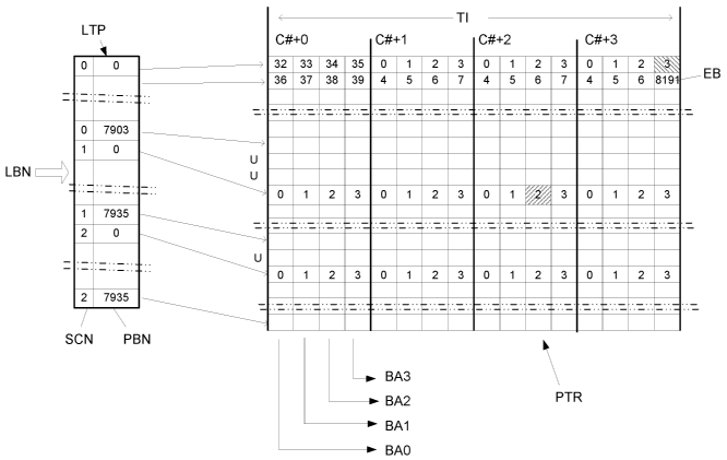
In Fig.3 the structure of the two tables LTP and PTR is shown. In the first
table for
address conversion LTP the logical block number LBN is converted into the
address of
a physical block, which consists of the components superchip number SCN and
physical
block number PBN. In the example presented here three superchips with the
numbers 0
to 2 are present. The superchip number is thus 2 bits long. A physical block
number
consists of thirteen bits and can take values from 0 to 8191 thereby. In order
to leave
space for 32 administrative blocks and in each case 256 reserve blocks, the
values can
go up only to 7903 or respectively to 7935.
As shown in Fig. 2, the logical block number LBN in this example is 16 bits
long and
can take on values between 0 and 24319, according to the sum of the physical
blocks of
the three superchips SCO to SC2.
The pointers from the first table LTP serve as index in the second table PTR.
They point
in each case to a tuple of sixteen real blocks, which are arranged in four
times four
banks BAO to BA3. A tuple is arranged in four chips of a superchip. Thus a
table with
16 columns results, in which the real block numbers of a bank are indicated
respectively. Values between 0 and 7903 or 7935 respectively can be indicated,
as long
as no spare blocks were registered. In this manner for instance a spare block
EB is
registered in the second line at last position, which has then a larger block
number. The
block numbers can only have values modulo of the bank number. By
administrative
operations however, the block numbers can arbitrarily be interchanged within
the banks.
The lines of the table PTR, which can not be addressed with the aid of a
physical block
number, are unused, here characterized by a U in each case.
The real memory blocks, which can be addressed by the two examples from Fig.
2, are
marked in the table by shading. The logical sector number LSN = 127 addresses
here
the block 3 in the first line of the table PTR over SCN = 0 and PBN = 0 with
the tuple
index TI = 15, and belongs to chip 0*4+3 = 3. The logical sector number LSN =
1011769 addresses here the block 2 over SCN=1 and PBN=O with the tuple index
TI =
10, and belongs to chip 1 *4+2 = 6.
CA 02591957 2007-06-26
WO 2006/072549 - 6 - PCT/EP2005/056985
Reference signs
BAn - memory bank number
Cn - chip number
EB - spare block
LBN - logical block number
LSN - logical sector number
LTP - first allocator table (logtophys)
PBn - physical block number
PTR - second allocator table (phystoreal)
RBN - real block number
RSN - real sector number
PN - page number
PSN - physical sector number
SCn - super chip number
SN - sector number
TI - tuple index
U - unused physical blocks