Note: Descriptions are shown in the official language in which they were submitted.
CA 02592187 2007-06-18
HARD FILM AND METHOD OF MANUFACTURING THE SAME
BACKGROUND OF THE INVENTION
1. Field of the Invention
The present invention relates to a hard film, which is formed on
a surface of a cutting tool such as a tip, a drill, and an end mill,
and a surface of a plastic working tool such as a forging die and a
punch for improving wear resistance of the tools, and relates to a method
useful for manufacturing such a hard film.
2. Description of Related Art
Usually, coating of a hard film of TiN, TiCN, TiAlN or the like
has been performed for the purpose of improving wear resistance of a
cutting tool using sintered hard alloy, cermet, or high speed tool steel
as a base material. In particular, since a composite nitride of Ti and
Al (hereinafter, abbreviated as "TiAlN") exhibits excellent wear
resistance as disclosed in Japanese Patent No. 2644710, a film of the
composite nitride is increasingly used for a cutting tool for cutting
a very hard material (work material) such as a high speed cutting
material or hardened steel in place of a film including nitride (TiN)
or carbonitride (TiCN) of Ti.
However, a film further improved in wear resistance is now
required with recent increase in hardness of work material or increase
in cutting speed.
The hard film is further required to have oxidation resistance
under high temperature. In the TiAlN film as above, oxidation
resistance is comparatively high, and oxidation starts near 800 to 900 C,
1
CA 02592187 2007-06-18
however, there is a difficulty that deterioration of the film tends
to progress under a more severe environment. Therefore, a hard film
is proposed, in which the TiAlN film is added with Cr, thereby the
concentration of Al is increased while keeping a cubic crystal structure
with high hardness, and consequently oxidation resistance is further
improved (e.g., JP-A-2003-71610) . Moreover, a hard film is proposed,
in which oxidation resistance is further improved by adding Si or B
into a TiCrAlN film (e.g., JP-A-2003-71611), or a hard film is proposed,
in which oxidation resistance is further improved by adding Nb, Si or
B into a CrAlN film (e.g., W02006-005217) is proposed.
However, the hard films proposed so far cannot be regarded to be
excellent in wear resistance and oxidation resistance, and actually,
further improvement in properties is desired.
SUMMARY OF THE INVENTION
In view of foregoing, it is desirable to provide a hard film that
is obviously excellent in wear resistance, and exhibits excellent
oxidation resistance even under a condition that hot heat generation
easily occurs due to friction heating, consequently exhibits excellent
properties compared with a usual hard-film including TiAlN, TiCrAlN,
TiCrAlSiBN, CrAlSiBN, or NbCrAlSiBN, and provide a method useful for
manufacturing such a hard film.
A hard film of an embodiment of the invention is summarized in
that it includes (M) aCrbAl,SidBeYfZ (however, M is at least one element
selected from a group 4A element, a group 5A element, and a group 6A
element (except for Cr) in the periodic table, and Z shows one of N,
2
CA 02592187 2009-06-25
CN, NO and CNO), wherein
a+b+c+d+e+f=l,
0<a:~0.3, 0 . 0 5<-b<-0 . 4, 0.4<-c<-0.8, 0<-d<-0.2, 0<-e<0.2,
0.01:~f:~0.l,and at least one of d?0.03 and e_0.03 (a, b, c, d, e
and f show atomic ratios of M, Cr, Al, Si, B and Y respectively).
Moreover, such a subject can be achieved by a hard film
including CrbAl~SiaBeYfZ (however, Z shows one of N, CN, NO and
CNO), wherein
b+c+d+e+f=l,
0.2<-b_0.5, 0.4<-c<-0.7, 0<-d<-0.2, 0<-e<-0.2, and 0.01<-f<-0.1
(however, d+e>0),
(b, c, d, e and f show atomic ratios of Cr, Al, Si, B and Y
respectively).
As a preferable mode of the hard film of an embodiment of
the invention, a hard film is given, in which hard films as above
(within a composition range shown as above) are alternately
stacked with compositions being different from each other, and
thickness of each layer is between 5 nm and 200 nm.
When the hard film as above is manufactured, the hard film
is preferably formed by a cathode discharge arc ion plating
method.
Advantage of the Invention
The hard film of an embodiment of the invention is in a hard
film structure as expressed by a certain expression, thereby a
hard film can be achieved, in which wear resistance is obviously
excellent, and deterioration in property due to oxidation is not
caused even under a condition that hot heat generation easily
occurs due to friction heating. Such a hard film is extremely
useful as a hard film formed on surfaces of base materials of
various cutting tools, or plastic
3
CA 02592187 2007-06-18
working tools such as a forging die and a punch.
BRIEF DESCRIPTION OF THE DRAWINGS
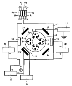
Fig. 1 is a schematic illustrative diagram showing a configuration
example of an arc ion plating apparatus (AIP apparatus) for
manufacturing the hard film of an embodimerlt of the invention.
DESCRIPTION OF THE PREFERRED EMBODIMENT
The inventors made investigation from various points of view to
further improve high-temperature resistance (oxidation resistance) of
a hard film. As a result, they found that Cr was contained as an
indispensable component, and Y was contained in place of Si or B being
regarded to be effective for improving oxidation resistance, or
contained in addition to Si or B, leading to extreme improvement in
oxidation resistance of a hard film, consequently completed an
embodiment of the invention. Hereinafter, a reason for selecting each
element in the hard film of an embodiment of the invention, and a reason
for limiting a composition range of each element are described.
The hard film of an embodiment of the invention is expressed by
the following general expression (1). A reason for selecting each
element in the hard film of an embodiment of the invention, and a reason
for limiting a composition range of each element are described.
(I"!) aCrvAlcSldBeYfZ =o= (1) i
(a, b, c, d, e and f show atomic ratios of M, Cr, Al, Si, B and Y
respectively, and Z shows one of N, CN, NO and CNO).
A metal element M is at least one element except for Cr selected
4
CA 02592187 2007-06-18
from a group 4A element, a group 5A element, and a group 6A element
(Ti, Zr, Hf, V, Nb, Ta, Mo and W) in the periodic table. The metal element
exhibits an operation of forming a nitride (MN) having high hardness
in a film, and thus increasing film hardness. However, since nitrides
of the elements are bad in oxidation resistance compared with CrN, large
content of the metal element M reduces oxidation resistance of a film.
Therefore, an upper limit of an atomic ratio of M in the film needs
to be 0.3 (that is, when a+b+c+d+e+f=l is given, a needs to be 0.3 or
less).
Moreover, when the metal element M is not contained at all,
hardness tends to be slightly decreased, therefore a lower limit of
the metal element is more than 0 (that is, a>0). A preferable range
of the metal element M is 0. 02 to 0.2 in the light of oxidation resistance
and hardness. As the metal element M, Ti or Hf is preferably selected
in the light of hardness, and Nb is preferably selected in the light
of oxidation resistance and hardness.
The hard film of an embodiment of the invention contains Cr as
an indispensable component. Cr is a necessary element for configuring
the film to improve oxidation resistance of the film, and dissolve A1N
in a CrN nitride of a cubic rocksalt type to form metastable cubic A1N.
A lower limit of an atomic ratio of Cr needs to be 0.05 (that is, a
subscript b is not less than 0.05) in the hard film so that Cr exhibits
such effects. However, CrNislowin hardness compared with the nitrides
of M, and excessive content of Cr may cause reduction in hardness of
a film. Therefore, an upper limit of Cr is 0.4 (that is, b<_0.4). A
preferable range of the Cr content is in a range of 0.1 to 0.25 in an
CA 02592187 2009-06-25
atomic ratio (0.1<_b<_0.25).
Al is an element necessary for improving oxidation resistance of
a hard film, and needs to be contained in an atomic ration of 0.4 or
more (that is, c?0.4) to exhibit such an effect. However, since a stable
phase of AlN primarily includes a hexagonal structure, when Al is
excessively contained and significantly exceeds the total sum of added
amount of metal elements M and Cr, transfer into a hexagonal structure
occurs, resulting in softening of a film. Therefore, an upper limit
of an atomic ratio of the content of Al needs to be 0.8 (that is, c<_0.8) .
A preferable range of the Al content is 0.5 to 0.6 in an atomic ratio
( 0 . 5<_c<_0 . 6) .
Si, B and Y are added in a film with an upper limit of 0.2 (0.1
in the case of Y) in an atomic ratio to improve oxidation resistance
respectively. Since Y has the largest effect of improving oxidation
resistance among them, Y needs to be added in an atomic ratio of 0.01
or more (that is, f_0.01).
Addition of Si and B provides an operation of fining crystal grains
of a film and thus increasing hardness, in addition, when Si and B are
contained together with Y, an effect of further improving oxidation
resistance is provided. Si and B are preferably added in an atomic ratio
of 0.03 or more (that is, d_0.03, e_0.03) to exhibit such effects
respectively. However, since addition of the elements tends to cause
a film to be transferred into an amorphous or hexagonal structure, upper
limits of them are specified to be 0.2 in Si, 0.2 in B, and 0.1 in
Y(that is, d50.2, e<0.2, and f<0.1) respectively. As a more preferable
6
CA 02592187 2007-06-18
range, Si of 0.03 to 0.07, B of 0.05 to 0.1, and Y of 0.02 to 0.05 are
given.
The hard film of an embodiment of the invention may include any
form of a nitride, carbonitride, nitrogen oxide, and carbon-nitrogen
oxide (Z is N, CN, NO or CNO in the general expression (1)). However,
preferably, the form is essentially a nitride, and a ratio (atomic ratio)
of N in Z is 0.5 or more. More preferably, the ratio is 0.8 or more.
As an element other than N, C or 0 is contained as the remainder.
In an application requiring more improved oxidation resistance,
a composition of the hard film contains Cr and Y as indispensable
components as expressed in the following general expression (2), thereby
stability can be added at further high temperature.
CrbAlcSidBeYfZ =e= (2),
(b, c, d, e and f show atomic ratios of Cr, Al, Si, B and Y respectively,
and Z shows one of N, CN, NO and CNO).
In such a hard film, since the metal element M being a stabilizing
element of the cubic rocksalt structure is not present, a crystal
structure is easily transferred into a hexagonal structure in a case
of some Al content. Therefore, the content of Cr needs to be 0.2 or
more (that is, b20.2) to stabilize a cubic AlN compound. However, when
Cr is excessively contained, hardness is decreased even if a crystal
structure is cubic. Therefore, an upper limit of the content of Cr needs
to be 0.5 (that is, b_0.5). A preferable range of the Cr content is
about 0.3 to 0.4 in an atomic ratio (that is, 0.35bS0.4).
Regarding the Al content in the hard film, since the hexagonal
structure is easily formed in the hard film, an upper limit of the Al
7
CA 02592187 2007-06-18
content is specified to be 0.7. More preferably, it is 0.5 to 0.6 (that
is, 0.55c<-0.6). Regarding Si, B and Y, a specified range and a
preferable range are the same as in the hard film expressed in the general
expression (1) . However, at least one of Si and B needs to be contained
(that is, d+e>0) in the light of fining of film crystal grains and
increase in hardness by adding Si or B.
The hard film of an embodiment of the invention needs not be wholly
configured by a film having a single composition, but may be a hard
film of a stacked type in which at least one or two layers are stacked,
the layers having different compositions from one another in the
composition range of the general expression (1) or (2) . As an example
(combination) of such a stacked-type hard film, TiCrAlSiYN/NbCrAlYN,
TiCrAlBYN/HfCrAlYN and the like are given. In these examples,
compositions of the films are made different from each other by changing
kinds of elements configuring the respective films. However, even in
a combination of the same element, compositions can be made different
from each other by differing composition ranges from each other.
When the films different in composition or element are stacked
as above, since lattice constants of the films are different from each
other, lattice distortion is induced between layers, leading to further
increase in hardness of the films. In the case that the films are stacked,
thickness of each layer is preferably 5 nm or more, and when the thickness
is less than 5 nm, the films exhibits the same performance as that of
a film having a single structure. When thickness of each layer exceeds
200 nm, since the number of stacking is decreased because thickness
of about several micrometers is required for a cutting tool or other
8
CA 02592187 2007-06-18
tools, the number of interfaces in which distortion is stored is
decreased, consequently the effect of increase in hardness is hardly
obtained. More preferably, thickness of each layer is about 10 to 100
nm.
While a method of manufacturing the hard film of an embodiment
of the invention is not particularly limited, a PVD method using a solid
target is recommended for the method. In particular, the cathode
discharge arc ion plating method (AIP method) is preferably used. In
formation of the hard film of a multi-component system as above, if
a sputtering method is used, difference in target composition is
increased between a target composition and a film composition. However,
such a difficulty of difference in composition is substantially
eliminated in the AIP method. Moreover, there is an advantage that since
an ionization ratio of a target element is high in the AIP method, a
formed film is tight and high in hardness.
In the hard film of an embodiment of the invention, the hard film
is provided as a stacked film in which films are stacked, the films
having compositions as shown in the general expression (1) or (2)
respectively, thereby film performance can be improved. However, the
stacked film can be configured by combining a film having the relevant
composition and a hard film having a composition other than the film
composition as shown in the general expression (1) or (2) . For example,
the film can be configured by stacking a film including a nitride,
carbide, or carbonitride of at least one element selected from a group
including a group 4A element, a group 5A element, and a group 6A element
in the periodic table, and Al, Si, and B, and a film having a composition
9
CA 02592187 2007-06-18
as shown in the general expression (1) or (2) . As such a film, a film
of TiAl(CN), TiCrAl(CN), CrAl(CN), TiSi(CN), TiVAl(CN), TiNbAl(CN),
NbCrAl(CN) or the like is exemplified.
Fig. 1 is a schematic illustrative diagram showing. a configuration
example of an arc ion plating apparatus (AIP apparatus) for
manufacturing the hard film of an embodiment of the invention. In the
apparatus shown in Fig. 1, a turntable 2 is disposed within a vacuum
chamber 1, and four rotation tables 3 are symmetrically attached to
the turntable 2. Each rotation table 3 is mounted with a body to be
treated (base material) 5. Around the turntable 2, a plurality of (two
in Fig. 1) arc evaporation sources 6a, 6b (cathode side), and heaters
7a, 7b, 7c and 7d are disposed. Arc voltage sources 8a, 8b are disposed
at respective sides of the evaporation sources 6a, 6b to evaporate the
sources respectively.
In the figure, 11 is a filament-type ion source, 12 is an AC power
supply for filament heating, and 13 is a DC power supply for discharge,
wherein a filament (made of W) is heated by current from the AC power
supply for filament heating 12, then emitted thermoelectrons are
introduced into the vacuum chamber by the DC power supply for discharge
13, so that plasma (Ar) is generated between the filament and the chamber
to generate Ar ions. Cleaning of the body to be treated (base material)
is performed using the Ar ions. The inside of the vacuum chamber is
configured in such a way that the inside is evacuated to a vacuum by
a vacuum pump P, and various kinds of deposition gas is introduced
through a mass flow controller 9a, 9b, 9c or 9d.
Targets having various compositions are used for the respective
CA 02592187 2007-06-18
evaporation sources 6a, 6b. The turntable 2 and the rotation tables
3 are rotated while the targets are evaporated in a deposition gas
(C-source-contained gas, 02 gas, and N-source-contained gas, or diluted
gas of them with inert gas) using the filament-type ion source 11,
thereby hard films can be formed on a surface of the body to be treated
5. In the figure, 10 is a bias voltage source provided for applying
a negative voltage (bias voltage) to the base materials 5.
The hard film of the stacked type can be achieved (1) by using
a plurality of different arc evaporation sources 6a, 6b, in addition,
it can be achieved (2) by periodically changing a negative voltage (bias
voltage) applied to the body to be treated 5, or (3) by changing an
atmospheric gas. In particular, a ratio of the C-source-contained gas
in the atmospheric gas is periodically changed to stack at least two
kinds of films having values of carbon in the expression (1) being
different from each other.
Control of a period of the hard film of the stacked type (repetition
period of stacking) and thickness of each layer can be achieved by
controlling rotation frequencies of the turntable and rotation tables
and input power for the respective evaporation sources (proportional
to the amount of evaporation) in the (1), time for applying the bias
voltage in the (2), and time for introducing the atmospheric gas in
the (3).
As a base material for forming the hard film of an embodiment of
the invention, sintered hard alloy, cermet, cBN or the like is given
as an applicable tool material, the hard film can be applied to an
iron-based alloy material such as cold-worked tool steel, hot-worked
11
CA 02592187 2007-06-18
tool steel, or high speed tool steel.
While the invention is described more specifically with examples
hereinafter, it will be appreciated that the invention is not restricted
by the following examples, and the invention can be obviously carried
out with being appropriately altered or modified within a scope suitable
for the content described before and after, and all of such alterations
or modifications are encompassed within a technical scope of the
invention.
Examples
Example 1
A target containing M, Cr, Al, Si, B and Y in various ratios was
disposed on the arc evaporation source 6a of the apparatus (AIP
apparatus) shown in Fig. 1, and a super-alloy tip, a super-alloy boll
end mill (10 mm in diameter, two flute) as the bodies to be treated
5, and a platinum foil for an oxidation test (30 mm in length, 5 mm
in width, and 0.1 mm in thickness) were mounted on the rotation tables
3, then the inside of the vacuum chamber was evacuated into a vacuum.
Then, the bodies to be treated 5 were heated to a temperature of 550 C
by the heaters 7a, 7b, 7c and 7d disposed within the vacuum chamber
1, and subjected to cleaning using Ar ions (Ar, pressure of 0.6 Pa,
voltage of 500 V, and time of 5 min), and then nitrogen gas (N2 gas)
was introduced to increase pressure in the chamber 1 to 4.0 Pa to start
arc discharge, consequently hard films 3 m in thickness were formed
on surfaces of the bodies to be treated S. When C or 0 was contained
in the film, methane gas (CH4 gas) or oxygen gas (02 gas) was introduced
into the deposition apparatus in a range of flow ratio to N2 gas of 5
12
CA 02592187 2007-06-18
to 50 in volume percent. During deposition, a bias voltage of 20 to
100 V was applied to a substrate such that electric potential of the
bodies to be treated 5 is negative with respect to ground potential.
For obtained hard films, metal compositions in the films were
measured by EPMA, and Vickers hardness (load of 0.25 N, and holding
time of 15 sec) was investigated. Moreover, crystal structures of the
films, and characteristics (oxidation start temperature, and wear
width) of the films were evaluated.
Analysis Condition of Crystal Structure
Evaluation of the crystal structures were performed by X-ray
diffraction in e-29 using an X-ray diffraction apparatus manufactured
by Rigaku Corporation. At that time, X-ray diffraction for a cubic
structure was performed using a CuKa radiation source, and peak
intensity for (111) face was measured near 26=37.78 , peak intensity
for (200) face near 26=43.9 , and peak intensity for (220) face near
20=63.8 . X-ray diffraction for a hexagonal structure was performed
using the CuKa radiation source, and peak intensity for (100) face was
measured near 20=32 to 33 , peak intensity for (102) face near 20=48
to 50 , and peak intensity for (110) face near 26=57 to 58 . A crystal
structure index X was calculated using values of them according to the
following expression (3), and crystal structures of the films were
determined according to the following standard.
(IB(111)+IB(200)+IB(220) ) / (IB(111)+IB(200)+IB(220)+IH(100)+IH
(102)+IH(110) ) === (3),
wherein IB (111) , IB(200) and IB(220) show peak intensity of
13
CA 02592187 2007-06-18
respective faces of the cubic structure. IH(100), IH(102) and IH(110)
show peak intensity of respective faces of the hexagonal structure.
A case of the index X of 0.9 or more: cubic crystal structure (in
the following tables, described as Bl)
A case of the index X of not less than 0.1 and less than 0. 9: mixed
type (in the following tables, described as Bl+B4)
A case of the index X of less than 0. 1: hexagonal crystal structure
(in the following tables, described as B4)
Oxidation Start Temperature
A platinum sample obtained in the example (platinum foil having
a hard film formed thereon) was heated from room temperature at a heating
rate of 5 C/min in artificial dry air, and change in mass of the sample
was investigated by a thermobalance. Oxidation start temperature was
determined from an obtained mass increase curve.
Using a test end mill obtained in the example (ball end mill made
of sintered hard alloy having a hard film formed on a surface thereof) ,
cutting was performed at the following cutting conditions with SKD 11
(HRC60) as a work material, then an edge was observed by a light
microscope to measure wear width of a boundary portion between a cutting
face and a flank.
Cutting speed: 150 m/min
Cutter feed: 0.04 mm/cutter
Axial cutting depth: 4.5 mm
Radial cutting depth: 0.1 m/s
Cutting length: 50 m
down cut, dry cut, and air blow only
14
CA 02592187 2007-06-18
Results of them are shown in the following Tables 1 and 2 together
with the compositions of the hard films.
CA 02592187 2007-06-18
m
5y. ¾t¾t r ~, m_ = a_
. . N N co l6 m p O `p O
E N N N N N O V i) z
p~ N O
> > > > > w ui W
:D :3 7 Z) w
0
C 0 O O O 0 O LO O O tn O u> O O 0 M in in O 0 in O 0 O 0 in O LO LO
ID 00 0) OD It P') M M <O N N M ~ CD N N M ~t (O N t0 M N N M It CO
U
B
~ a> O O O O 0 O O O O O O O O O O O O O O O O O O O O O O O O
Om O O O 0 O O 0 O 0 O 0 O O 0 O 0 0 0 0 O M 0 O 0 lD ~f1 tn tn
~ O O N N M M M N N N O N N N N N
r r r r r r r r r'- r r r r r r r r r r r.- r r r r r
v a`~ r
O
O O O O 0 O O O O O O O O O O O O O O O O O O O O O O O O
O O O O O O O O O O O O O lD O O~ lD O O O M O O O Om O O
. '? S Op p 0) p) 0) 00 N M N N (, C') M N N 00 N N P') N 00 M 0) r N M r r 00
N M N N N N M M M M N M M M M N M M M M N M N M M C) M M N
_
U m m C~ CD m Cfl Cfl CO CO C~ m CD C~ m m m CO m C~ +(fl C~ CD m 0] Cfl 47 +
N m m
O O O O O 0 O O O O O O O O O O O O O O O O O O O O O O O O
r r r r r r r r r r r.- r r r r r r r r r r r r r r r r
Z
U o O 0 O 0 O o O O O O o O O O O O O O O O O O O O O O O O
E
r r r r r r r r r r r r r r r r r r r r r r r r r r r r
U)
'. . ~ N lf) O lD N N N N N N N N N N N M CM M M M M M
o ~ O O O O O p O O r O O O O O O O O 00 O O O O O O O O
O O O O O O O O O O O O O O O O O O O O O O O
. '. N LO N O 0 N
CO O O O O O O O O O O O O O O O O O O N N O O O O O O O O
- O O O O O O
2
ln l!) LO M 1~ N O ln M
. . O O O p 0 p O O O O O O O r N N O O O O O O O O O O O O O
O O O O O O O O 111 0
Ln in Ln 0 O O r h N O O m O O O r aD r O O OD ~ O O O O O 0
- 0 ID LO ID (O t0 (O tfl lD W (O 0 0 0 0 t0 0 0 0 0 0 M ~t 0 0 I, CO OD
. a O O O O O O O O O O O O O O O O O O O O O O O O O O O O O
LO ~ d ~ N N M I- M N N N 0 M N t, N f~ O ln O n
p r 0 O N N N N N N N N r r N N N r r N M M N N r r 0
0 610 o p O o O O o 0 0 0 0 0 0 o o 0 0 o O o 0 0 0 o O
H F- F F H F F 1- F- F= F I F H I F F F= H F F H 1- H t F H H
~ ~
. . ~t N N 0 W W W ('M d d' M ~F M O M M M M O M tn LL) O I~ N I~ tl)
[t M r N N N 0 0
O O O O O O O O O O O O O O O O O O O O O O O O O O O O
~O N M d' In CO I~ 00 ~ O N M d' Ln (O I, 00 0)
z L N M ~ W W r OC) N N N N N N N N N
M
16
CA 02592187 2007-06-18
U
N z
W W
W
O O OLn O LO tn O O O LO O r O OLn O O tn tfl tn O u) O O O Lo LO 0 Ln 0 LO
r d M N M M 00 00 V M N M(O V M M N M M M N M N M N N N V N N M V
O O O O O O O O O O O O O O O O O O O O O O O O O O O O O O O O
. p~ 0 Li) O OLO O O O lC1 LO O O OLf) O O O O tn LO LO OLfl 0 LO O O Lf) tfl
tf) tf) tn
-~ m O N N N O N N N N N O ~ N ~ M N.- ~ N N N N N N N N N N N
U
O O O O O O O O O O O O O O O O O O O O O O O O O O O O O O O O
c S u') O O V1 O O O O ln O O N O LO O LO LO LO N LO O tC) O O tn L17 l() U)
LO 1f) lf) Lf1
0) N N N 0) 00 N() M . - -- N N M N N N M N N C7 M M C) M M M M
N M M M M N N C`7 M M M M M M M M M M M M M M C) M M M M M M M M
a> _
~ m m m m m m m m m m m m m m m m m m m m m m m m m m m m m m m m
U N
N M 7
O O O O O O O O O O O O O O O O O O O O O O O O O O O O O
O O O O
. ,. rn 00 r rn m r cD
z
. . O O O O O O O
N C'M
U O O O O O O O O O O O O O O O O O O O O O O O O 0 O O O O
O O O
E . r- '-- . . . . . f-
M
M M C`) C`') M M M M M M M M M C) C) M(`7 M M M(`') M M M C) M M M M C7 M C`7
. ~, O O O O O O O O O O O O O O O O O O O O O O O O O O O O O O O O
010 O O O O O O O O O O O O O O O O O O O O O O O O O O O O O O
0
E C~ O O O O O O O O O O O O O O O O O O O O O O O O O O O O O O O O
0
m
E
O O O O O O O O O O O O O O O O O
2 ~
in tn in U~ r r oo rin r r r r r r r r r r r r r r r r r r ~
1P) O ~ ln LO LO ln 1n LO tf) ~ LO LO l!) tn LO LO !n L() LO tf) LO LO LO U)
LC) LO ln N tf)
.- O .- O .- O O ~ O O O O O O O O O O O
'. Q O O O O O O O O O O O O O O O O O O O O O O O O O O O O O O O O
l() ln t() a ~ LO LO N N r t() LO LO U) U) lfl LO lf) LO lf1 LO LO If) ln ln
ln l(/ LC) lfi
O O '- ~ N M N N N N N N N N N N N N N N N N N N N N
U ~ O ~ p O O O 0 p O O O O O O O O O O O O O O O O O O O O O
~-- O
F _
. .. ~ N N r r r N r O~~ ~~~~ tn tn tn ln L[) ln ln ln ln tn
~ M N N r- ~ O O ~ - - - '- .- - r-
O O O O O O O O O O O O O O O O O O O - - - - O O O O O O 11010
O O O O
N
2 ln (O r 00 M O N (7 LO CO r 00 O O - N M V LO (0 r CO 0) O ~
-a Z M M M M M M M M M Vk V V V V V~t V' V Ln lS7 LC) tf) U) LO LO Lf1 L() !n
(D (O
17
CA 02592187 2007-06-18
Sample Nos. 6 to 10, 12 to 15, 17 to 20, 22, 24 to 29, 31 to 35,
38 to 41, and 43 to 61 in the Tables 1 and 2 correspond to hard films
satisfying requirements specified in an embodiment of the invention,
and the hard films are excellent in hardness, oxidation start
temperature, wear width and the like compared with usual hard films
(Nos. 1 to 5) and hard films varied from the requirements specified
in an embodiment of the invention (Nos. 11, 16, 21, 23, 30, 36, 37,
41 and 42).
Example 2
A target containing Cr, Al, Si, B and Y in various ratios was
disposed on the arc evaporation source 6a of the apparatus (AIP
apparatus) shown in Fig. 1, and a super-alloy tip, a super-alloy boll
end mill (10 mm in diameter, two flute) as the bodies to be treated
5, and a platinum foil for an oxidation test (30 mm in length, 5 mm
in width, and 0.1 mm in thickness) were mounted on the rotation tables
3, then the inside of the vacuum chamber was evacuated into a vacuum.
Then, the bodies to be treated 5 were heated to a temperature of 550 C
by the heaters 7a, 7b, 7c and 7d disposed within the vacuum chamber
1, and subjected to cleaning using Ar ions (Ar, pressure of 0.6 Pa,
voltage of 500 V, and time of 5 min), and then nitrogen gas (N2 gas)
was introduced to increase pressure in the chamber 1 to 4.0 Pa to start
arc discharge, consequently hard films 3 m in thickness were formed
on surfaces of the bodies to be treated 5. When C or 0 was contained
in the film, methane gas (CH4 gas) or oxygen gas (02 gas) was introduced
into the deposition apparatus in a range of flow ratio to N2 gas of 5
to 50 in volume percent. During deposition, a bias voltage of 20 to
18
CA 02592187 2007-06-18
100 V was applied to a substrate such that electric potential of the
bodies to be treated 5 is negative with respect to ground potential.
For obtained hard films, metal compositions in the films were
measured by EPMA, and Vickers hardness (load of 0.25 N, and holding
time of 15 sec) was investigated. Similarly as in the example 1, crystal
structures of the films, and characteristics (oxidation start
temperature, and wear width) of the films were evaluated.
Results of them are collectively shown in the following Table 3.
It is known that hard films satisfying the requirements specified in
an embodiment of the invention (sample Nos. 66 to 69, 71 to 74, 77 to
80, 85 to 87, and 89 to 91) are excellent in hardness, oxidation start
temperature, wear width and the like compared with usual hard films
(sample Nos. 62 to 65) and hard films varied from the requirements
specified in an embodiment of the invention (sample Nos. 70, 75, 76,
81 to 84, and 88).
19
CA 02592187 2007-06-18
r in a c~
~ ` oy 0c 5 ~
> > > > w LU LU w
N N N N
n D W
0
~ O) 00 OD tn ~ r- N 0 1~ CC) In N 0 0 0 1~ ~ t0 0 0 0 0 0 (0 n 0 t, ln 0~
. '. 0 O O O
7 M M M t0 N N N V l0 l0 M N N N 1~ 00 OD ~ ~t N N I~ N N N
3
a) O O O O O O O O O O O O O O O O O O O O O O O O O O O O O O
0 O O ln O O
otj O O O O t) O l() i!) O O tP1 ln 0 O M O O 0 0 0 ~ O O 0
O O r- N M M M r- N N CM N N O CM M M M N N ~ M N M M ~ ~ N N
0
O O O O O O O O O O O O O O O O O O O O O O O O O O O O O O
a) S O O O O O ~n N 0 O O O 0 O O O O O O O O in u~ O O O O O ~n ~n
' ~ S 00 0) W O) .- ~ '- ~ 1~ M M N N 00 O) ~ N M '- 0) OD 00 ~ N r- O) Q) N N
~~' N N N N M M M M N M M M M N N M M M M N N N M M M N N M M M
m m m m m m m m m m m m m m m m m m m~~ m m m m m m m m m
U N
O O O O O O O O O O O O O O O O O O O O O O O O O O O O O
O O
m co n m c0
z O O O O O
U O O O O O O O O O O O O O O O O O O O O O O O 00 O O O O O 11
Z,
M
N ~ N l() lD N N N N N M C) C'M M M M M M M M M M M N N N
>- O O O O O O O '- ~ O O O O O O O O O O O O O O O O O O O O O
O O O O O O O O O O O O O O O O O O O O O O O O O O O
LO N M
m O O O O O O O O O O O O O O O O O O O O O O O O O O O O 0
p O O O
tn C') M M C) C) M 1~ N In ~ V It 7 V <t 7 N LO N N N N C`7 N N
1 ~ N O- O O O O O O O O O ~ N N O O O O O O O O O O O O O O O O
O O O O O O O O O O O O O O O O O O O O O O O O O O O O
0 0 0 1f) ~ t0 LO ln N (0 ~ LO In lf) c.~ ) V l!) (O 1, 00 00 00 ~ ~ LO M (O
t0 (O
O O O O O O 0 0 0 O 0 0 0 O O 0 0 o O O O
0 0 0 0 0 0 0 0 0
. . . C ~ L. a M ~ N LO (O <O [0 M 00 M M M M C") CO l!) a ~t M
a a
C") M C'M M M CC) C`') M N N lf) Ln 4 M N .- O ~ N N It LO (0 M M M
O O O O O O O O O O O O O O O O O O O O O O O 6 O O O O O O
M
~ ~ ln (O 1~ a0 0) O - N M ~ ln (O I~ 00 01 O ~ N C) V ln fD 1~ 0D 01 O ~
Z N co C)co co co cfl co cfl co ~ ~ ~ ~ ~ ~ ~ r ~ ~ eo 00 ao ao co 00 0o co
co 00 rn rn
CA 02592187 2007-06-18
Example 3
The plurality of arc evaporation sources 6a, 6b were installed
in the apparatus (AIP apparatus) shown in Fig. 1, and stacked films
including films having compositions as shown in the following Table
4 were formed. At that time, the plurality of targets 6a, 6b were
simultaneously discharged, and the base materials (bodies to be treated
5) were mounted on the rotating rotation tables 3 such that the base
materials alternately pass through respective fronts of the arc
evaporation sources 6a, 6b, thereby the stacked films were formed. For
a stacked film having a long stacking period, the arc evaporation sources
6a, 6b were alternately discharged to form the stacked film. Other film
formation conditions were the same as those in the examples 1 and 2.
For obtained hard films, metal compositions in the films, Vickers
hardness, crystal structures of the films, and characteristics of the
films were evaluated in the same way as in the examples 1 and 2.
Results of them are collectively shown in the following Table 4.
It is known that all samples (sample Nos. 92 to 102) are excellent in
hardness, oxidation start temperature, wear width and the like.
21
CA 02592187 2007-06-18
0 U) 0 0 U) 0 tC) 0 0 1f) lC)
~~ C) N N N N C) ('7 N ~t t=) N
v 0 0 0 0 0 0 0 0 0 0 0
lf) 0 lf) 0 t() lf) ln t!) 0 0 lf)
0 m N N N N N N N N r N N
'G a`> r r r r r r r r r r r
O
~ O O O O O O O O O O O
c S O O U) l() l!) 0 l!) l!) 0 0 0
N f") (") M N N r N N N C)
= v C~ m M m C7 N) P7 C) C) (`') (`')
r r r r r r r r r r Cf
T~ m m m m m m m m m m m
O O O O O O O O O O O
0 0 0 0 0 0 0 0 0 0 0
O O O O O 00 O O O O O
~' (`~ f~') (~') (`~ C~') N C) C`') C) (`7 C~)
F
O O
tn O ~ M 0 f- ln ~ r r
M
0
~ O O O O O O O O O
WN LO LOLO N (`~ (`9 lA O N
r r
Z Z Z Z Z Z Z -Z Z
m M M M M M M M o Z z o 0 0 0 0 0 0 0
N o 0 0 0 0 0 o M M o
} } } } } } } } o o r
J o 0 0 o c o o } } o
~
.. Y a a a a a a a a a a a
- 'N N N N N N N O O N
i i i
O D U O O U O U o o U
0 0 0 0 0 0 o'
1- i- F- F- F- F- F- Z
'
O O O O O O O O O
N ln N O ~ N ('~ (`~ 0 O N
N
a z z z z z z z z Z
o O o O O O O O Z
a
Z ~ C
. (O O O O G G G C
} G
. J } } } } } } } o
Y a a a a a a a a a
L
V
U 0 U U O D U U ~ _N CS
N N -Z
Z
. ~... ~i `,
`14
O r N
N c) ~t tn c0 r oo rn O O O
~ Z O) O) d) O) d) 0) O) 4) r r r
22