Note: Descriptions are shown in the official language in which they were submitted.
CA 02592734 2007-06-29
WO 2006/076091 PCT/US2005/043917
METHODS AND APPARATUS FOR OPTICAL
WIRELESS COMMUNICATION
CROSS REFERENCE TO RELATED APPLICATIONS
5[001] This application is related to and claims priority from the United
States utility patent application having application no. 11/036,479, filed on
January 13, 2005.
FIELD OF THE INVENTION
[002] The present invention relates generally to optical wireless
communication, and in particular to wireless optical delivery of a video
signal.
BACKGROUND
[003] The preferred consumer digital video interfaces are High Definition
Multimedia Interface (HDMI) and Digital Visual Interface (DVI). DVI is
commonly used by PC equipment to drive digital video displays. DVI
typically supports 24-bit RGB at video rates up to 165MHz. A DVI driver
accepts 24-bit RGB data and serializes it into three serial channels. The
video clock is added as a fourth channel. As the RGB data is serialized, it is
encoded using an 8b/10b encoding scheme called Transition Minimized
Differential Signaling (TMDS). HDMI is backwards compatible with DVI.
It supports alternate (non-RGB) color spaces and includes the ability to
carry digital audio.
[004] As with DVI, HDMI data is encoded to represent active video periods
and control periods. In addition, HDMI includes a third entity called a
Data Island. Data Islands are used to communicate additional data during
the blanking interval. For example, data islands are used to send digital
audio data in HDMI.
[005] Data delivered using a DVI or HDMI interface may be encrypted
using High-Bandwidth Digital-Content Protection (HDCP).
Implementation of HDCP requires a set of unique secret device keys.
1
CA 02592734 2007-06-29
WO 2006/076091 PCT/US2005/043917
During authentication, the receiver will only receive content once it
demonstrates knowledge of the keys. Furthermore, to prevent
eavesdropping and stealing of the data, the transmitter and receiver will
generate a shared secret value that is consistently checked throughout the
transmission. Once authentication is established, the transmitter encrypts
the data and sends it to the receiver for decryption.
[006] Heretofore, DVI/HDMI data has only been deliverable using hard
wires due at least in part to the way the data source and the display device
need to communicate with each other. However, it may be desirable for a
consumer to want to place a display device (such as a flat-panel television)
on a wall opposite from the video source (e.g., receiver or DVD player). In
this case, the consumer would typically be required to purchase and install
DVI cabling from the video source to the display. However, this may be
both costly and present difficult installation issues.
[007] A wireless radio frequency (RF) system could be used between a
video source and a display device. However, there may be numerous
reasons for preferring a wireless optical configuration between a digital
video source and a display device. For example, the hardware required for
an optical wireless signal may be less complex than a RF system.
Moreover, a wireless optical solution is more secure since it will not
penetrate walls as with an RF system.
[008] Therefore, a wireless optical system which eliminates the need for
cabling between a digital video source and a digital video sink may be
desirable.
2
CA 02592734 2007-06-29
WO 2006/076091 PCT/US2005/043917
SUMMARY
[009] Methods and apparatus for optical wireless communication are
disclosed. In one embodiment, a system includes a video data source having
a source output, an optical wireless transmitter to receive video data from
the source output and encode the video data into a laser beam, and an
optical wireless receiver to receive the laser beam and to extract the video
data there from. The method further includes a display device having a
destination input, wherein the display device receives the video data from
the optical wireless receiver and presents a video display based on said
video data.
[010] Other aspects, features, and techniques of the invention will be
apparent to one skilled in the relevant art in view of the following detailed
description of the invention.
3
CA 02592734 2007-06-29
WO 2006/076091 PCT/US2005/043917
BRIEF DESCRIPTION OF THE DRAWINGS
[011] FIG. 1 is one embodiment of a system level diagram for a digital
video system in accordance with the principles of the invention;
[012] FIG. 2 is one embodiment of an optical transmitter capable of
carrying out one or more aspect of the invention ;
[013] FIG. 3 is one embodiment of an optical receiver capable of carrying
out one or more aspect of the invention;
[014] FIG. 4 is a more detailed diagram of the transmitter circuit of FIG. 2;
[015] FIG. 5 is one embodiment of an electro-optical interface between the
optical transmitter of FIG. 2 and the optical receiver of FIG. 3;
[016] FIG. 6 is a more detailed diagram of the receiver circuit of FIG. 2;
and
[017] FIG. 7 is one embodiment of a control-channel system implemented
in accordance with the principles of the invention.
4
CA 02592734 2007-06-29
WO 2006/076091 PCT/US2005/043917
DETAILED DESCRIPTION OF THE EXEMPLARY EMBODIMENTS
[018] One aspect of the invention is to provide a wireless optical video
system in which video content (e.g., DVI or HDMI) is wirelessly transmitted
between a digital video source and a display device. In one embodiment,
this wireless optical communication is accomplished using a laser, encoded
with the digital video data, directed from an optical transmitter to an
optical receiver. In another embodiment, the data to be communicated
includes high-definition video content.
[019] Another aspect of the invention is to use a collimating lens to focus a
wireless optical signal onto the focusing lens of a receiver. While in one
embodiment, the laser beam to be transmitted is between approximately 1/4
inch to approximately 1/2 inch, it should equally be appreciated that the
beam may equally have a thicker or thinner diameter.
[020] Another aspect of the invention is to provide the video data to the
display at the same resolution and with the same video clock speed as that
of the video source. For example, HDMI and DVI provide a mechanism for
the video source to query the video sink as to what video formats are
supported. Once queried, the video source may select the "best" video
format for sending video data to the display. This selected video format
may then be passed from the video source, through a wireless optical link,
and on to a display device.
[021] In one embodiment, the invention also makes use of a control
channel communication system to enable DVI and HDMI content to be
transinitted wirelessly. Heretofore, DVI/HDMI data has only been
deliverable using hard wires given that the data source and the display
device are required to actively communicate with each other. In one
embodiment, this control channel communication system is provided by a
low data-rate 2.4GHz RF link. It should further be appreciated that a
control-channel communication system may be implemented with an
5
CA 02592734 2007-06-29
WO 2006/076091 PCT/US2005/043917
alternate technology, such as for example an Infrared optical
communication link.
[022] While much of the following description is in terms of HDMI/DVI
content and system components, it should equally be appreciated that the
principles of the invention are not limited and such, and may be applied to
any other type of video content, such as serial digital interface (SDI) and
high-definition serial digital interface (HD SDI).
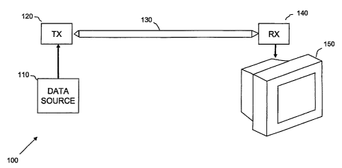
[023] Referring now to FIG. 1, depicted is a digital video system 100 usable
to implement one or more aspects of the invention. As depicted in FIG. 1, a
video source 110 may be coupled to an optical transmitter 120. In one
embodiment, the video source is an HDMI/DVI video source, such as an
ATSC tuner, DVD player, etc. In another embodiment, the video source 110
is a high-definition video source. In still another embodiment, the video
source 110 may be any known video source (e.g., HD SDI, 1080i, 720p,
480p, 480i, standard definition, etc.). Moreover, the signal provided to the
optical transinitter 120 by the video source 110 may be encrypted with a
copyright protection protocol, such as High-bandwidth Digital Content
Protection (HDCP).
[024] Continuing to refer to FIG. 1, in one embodiment the video source
110 provides video data to the optical transmitter 120, which in turn
provides a wireless optical signal 130 to optical receiver 140. As will be
described in more detail below, this optical signal 130 may be encoded with
the video data being provided by the video source 110. In one embodiment,
the optical signal 130 contains uncompressed high-definition video data.
Once the video data is received by receiver 140, it may be decoded for
display device 150.
[025] Transmitter 200 of FIG. 2 is a more detailed diagram of one
embodiment of the optical transmitter 120 of FIG. 1. Transmitter 200,
which receives the video signal from data source 110, is depicted as
including a DVI/HDMI receiver 210, a transmitter circuit 220, a system
clock 230 and a transmitter electro-optical interface 240. While in one
6
CA 02592734 2007-06-29
WO 2006/076091 PCT/US2005/043917
embodiment, the data source 110 is an HDMI or DVI video source (e.g.,
ATSC tuner, DVD player, etc.), it may similarly be another type of data
source.
[026] As depicted in FIG. 2, the data source 110 provides a digital signal to
the DVI/HDMI receiver 210. The DVI/HDMI receiver 210 may be used to
convert the DVI/HDMI digital signal from the data source 110 into a digital
video signal, such as 24-bit RGB. DVI/HDMI receivers are known in the
field and beyond the scope of this disclosure. In another embodiment, the
DVI/HDMI receiver 210 and the transmitter circuit 220 may be combined
into a single logical circuit. While in one embodiment, the transmitter
circuit 220 is a Field Programmable Gate Array (FPGA) or an Application-
Specific Integrated Circuit (ASIC), it may similarly have other
implementations. The other input for the transmitter circuit 220 comes
from the system clock 230, which provides a clock signal. In one
embodinient, this clock signal is a 110 MHz signal. The output of the
transmitter circuit 220 is to a transmitter electro-optical interface 240. One
embodiment of the transmitter circuit 220 will be described in more detail
below with reference to FIG. 4, while one einbodiment of the transmitter
electro-optical interface 240 is described in more detail below with reference
to FIG. 5.
[027] Receiver 250 of FIG. 3 is a more detailed diagram of one embodiment
of the optical receiver 140 of FIG. 1. In this embodiment, optical receiver
250, which receives the optical signal 130 from optical transmitter 120, is
depicted as including a receiver electro-optical interface 260, a receiving
circuit 270, a phase lock loop (PLL) 280, a DVI/HDMI transmitter 290, and
a system clock 300. The optical transmitter 250 is further depicted as
outputting video data to display device 150. While in one embodiment, the
digital video data output to the display device 150 is one of HDMI and DVI
data, it may similarly be another type of data.
[028] As depicted in FIG. 3, the optical receiver 250 includes a DVI/HDMI
transmitter 290, the details of which are known in the field and beyond the
7
CA 02592734 2007-06-29
WO 2006/076091 PCT/US2005/043917
scope of this disclosure. In another embodiment, the DVIIHDMI
transmitter 290 and the receiver circuit 270 may be combined into a single
logical circuit. As mentioned above, another input to the receiver circuit
270 comes from the system clock 300, which provides a clock signal. In one
embodiment, this clock signal is a 110 MHz signal. The transmitter circuit
270 is further depicted as being in communication with PLL 280, which
may be used to help regenerate the video clock of the DVI/HDMI
transmitter 290.
[029] Referring now to FIG. 4, depicted is a block diagram of one
embodiment of the transmitter circuit of FIG. 2. In this embodiment,
transmitter circuit 400 includes a front end 405 which may be used to
receive digital video data (such as 24-bit RGB) with control data from
HDMI/DVI receiver 210, and optional ancillary data. The front end 405
may then output a near continuous stream of data to the optional RS (Reed-
Solomon) Encoder 410. In one embodiment, this data is a 20-bit stream
output at 110MHz. If the incoming video data rate is insufficient to satisfy
the RS Encoder 410, null words may be generated such that the RS Encoder
410 is never starved for data. In one embodiment, the RS Encoder 410 may
be comprised of two 10-bit encoders that apply an RS code of (216,200). The
RS Encoders 410 may each accept 200 10-bit words of data and add 16
words of forward error correction (FEC) data. This coding scheme enables
the receiver to correct up to eight errors in each RS block of 216 words. In
another embodiment, forward error correction may not be performed.
[030] The RS Encoder may then output the data to the scrambler 415,
which randomizes the data. The scrambler 415 may randomize the data to
ensure that frequent transitions occur in the data stream. Frequent
transitions help the receiver 270 synchronize itself to the 2.2GHz bit clock
and recover the data. In one embodiment, the scrambler 415 may use a
pseudo-random number (PRN) generator to create a 20-bit random number
for each 20-bit word. The incoming word is exclusive-OR'ed with the
random number to produce a scrambled output. As will be described below,
8
CA 02592734 2007-06-29
WO 2006/076091 PCT/US2005/043917
an identical PRN generator may be used on the receiver-side to unscramble
the data.
[031] The header generator 420 may be used to output a word header. For
example, in one embodiment, every 20uS the header generator 420 may
output a 40 word header. A first portion of this header (e.g., first 20 words)
may be comprised of preset data used to synchronize the receiver, followed
by a second portion (e.g., next 20 words) of variable data, which can include
control information for the receiver-side.
[032] The serializer 425 receives the data stream from the header
generator, according to one embodiment. The serializer 425 is used to
accept the encoded data in parallel and shift it out a bit at a time. In one
embodiment, the serializer 425 outputs a high rate video data stream to the
transmitter electro-optical interface 240. The clock generator 430
synthesizes a clock (e.g., 2.2GHz) used by the serializer 425 for shifting the
parallel data though the system based on the clock signal 435 (e.g.,
110MHz) provided by a system clock (e.g., systein clock 230). 2.2GHz may
be used when electro-optical system 500 is tuned to operate at this specific
bit rate. A 2.2 GHz bit rate may be used because it is exactly 20 times the
110 MHz clock rate.
[033] Continuing to refer to FIG. 4, the controller 440 may be used to
synchronize the various components of the transmitter circuit 400. In one
embodiment, it may inform the header generator 420 when to generate a
header. It may also initialize the PRN generator in the scrambler 415.
Moreover, the controller 440 may also start the RS Encoder 410 such that
its output will be present at the proper time. In one embodiment, the
controller 440 may also inform the front end 405 when data must be
available to the RS Encoder 410. In the embodiment of FIG. 4, the
controller 440 outputs a clock to the video clock analyzer (VCA) 445. The
VCA 445 may be used to count the number of video clocks per time interval,
with the resulting count "n" being transmitted to the receiver-side as part of
9
CA 02592734 2007-06-29
WO 2006/076091 PCT/US2005/043917
the header's variable data. In one embodiment, "n" may be used on the
receiver-side to regenerate the video clock.
[034] Referring now to FIG. 5, depicted is a block diagram of one
embodiment of an electro-optical system 500, which includes the
transmitting electro-optical interface 240 of FIG. 2 communicating with the
receiving electro-optical interface 260 of FIG. 3. In this embodiment, the
transmitting electro-optical interface 240 provides an optical signal 550
which is received by the receiving electro-optical interface 260. In this
embodiment, the transmitting circuit 220 provides the video signal in the
form of a digital electrical signal to the laser driver 510 which, in turn,
generates a series of electrical potentials to the laser diode 520., This
sequence of electrical potentials is used by the laser diode 520 to convert
the
signal into an optical signal 550. Moreover, a collimating lens 530 may be
used to focus the optical signal 550 such that it is properly receivable by
the
receiving electro-optical interface 260.
[035] A focusing lens 540 may be used to capture and focus the optical
signal 550 onto a photo diode 560. The photo diode 560 receives and
converts the optical signal 550 into a digital electrical signal which may
then be passed to a trans-impedance amp 570 and then to a limiting amp
580.
[036] Referring now to FIG. 6, depicted is a block diagram of a particular
embodiment of the receiver circuit 270 of FIG. 3. In particular, data is
received by the receiver circuit 600 into a clock/data recovery block 610
from the receiver electo-optical interface 260. In one embodiment, the
function of the clock/data recovery block 610 is to extract the original
transmit clock (e.g., 2.2GHz) and divide it down to reproduce the
transmitter's system clock 230 (e.g., 110MHz) for use in moving the data
through the receiver circuit 600. Moreover, clock/data recovery block 610
may also deserialize the data to determine where one word ends and the
next begins within the serial data stream.
CA 02592734 2007-06-29
WO 2006/076091 PCT/US2005/043917
[037] The header detector 620 may be used to search for the headers
previously inserted by the transmitter circuit's header generator 420. When
the header is found, the header detector 620 may signal the controller 630
to synchronize itself with the data stream. Once synchronized, the
controller 630 may synchronize the other processing blocks in the receiver
circuit 600.
[0381 The remaining processing blocks in the receiver circuit 600 are
complementary to those in the transmitter circuit 400 of FIG. 4. For
example, the descrambler 640 may contain a PRN generator that is
initialized by the controller 630 at the proper tinie such that the data
following the. header is restored to its pre-scrambled values. The RS
Decoder 650 is used to decode the data, followed by final processing and de-
multiplexing by a back-end 660, which is complimentary to the previously-
described front end 405. In one embodiment, the backend 660 is responsible
for taking the data stream and extracting the original video and control
data.
[039] As previously mentioned, one aspect of the invention is to provide the
video data to the display 150 at the same resolution and with the same
video clock speed as that of the video source 110. For example, HDMI and
DVI provide a mechanism for the video source 110 to query the video
display 150 (sink) as to what video formats are supported. Once queried,
the video source 110 may select the "best" video format for sending video
data to the display 150. As will be described in more detail below, this
query communication may be performed over an 12C link.
[040] With that said, the electro-optical system 500 has no way of knowing
what video format will be selected by the video source 110. For tliis reason,
the electro-optical system 500 will be able to accommodate any arbitrary
clock rate, according to one embodiment.
[041] While it may be possible to first convert the incoming video data to a
standard format having a predetermined video clock rate, such an
additional conversion operation is undesirable due to the processing
11
CA 02592734 2007-06-29
WO 2006/076091 PCT/US2005/043917
overhead and image distortion inherent in such a conversion process.
Moreover, such a system would not be able to pass HDMI data due in part
to the fact that the video conversion process necessarily modifies the video
clock which would be needed by the display to extract data-islands in which
audio information is embedded. In addition, such a system would not
support the HDCP scheme. If the video data is encrypted, the display will
not be able to decrypt the data without the original video clock.
[042] Thus, in one embodiment, the video data is transmitted from the
video source 110 through the electro-optical system 500 and to the display
150 in what ever format and with the appropriate video clock, as
determined by the source 110. In one embodiment, this is accomplished by
regenerating the video clock in the receiver 140. The flow of video data
through the system is isochronous and the regenerated video clock must be
phase-locked to the source's video clock. Video clock regeneration may be
accomplished using a video clock counter in the transmitter (e.g., video
clock analyzer 445) and a special PLL (e.g., PLL 280) in the receiver coupled
to the video clock generator 680. At both the receiver and transmitter end,
the same 110 MHz clock signal is used as a reference. This 110 MHz clock
signal originates at the transmitter and is indirectly used to clock data
across the wireless optical link. In the transmitter, the controller 440
divides the 110 MHz clock down to create a 50 kHz clock. This 50 kHz clock
may then be used as a reference for the video clock analyzer 445. In the
receiver, the con.troller 630 divides the 110MHz clock down to create a
50kHz clock. This 50kHz clock is used as a reference for video clock
generator 680. The video clock generator uses the 50kHz reference clock
and the "n" value to regenerate the original video clock.
[043] As previously mentioned, one aspect of the invention is to use a
control channel communication system to enable content (e.g., DVI and
HDMI content) to be transmitted wirelessly. In one embodiment, this
control -channel communication system is provided by a low data-rate
12
CA 02592734 2007-06-29
WO 2006/076091 PCT/US2005/043917
2.4GHz RF link. Other embodiments may implement some of the control-
channel functionality in the optical link.
[044] In another embodiment, the RF link is used to perform required 12C
queries of the display. 12C is an interface used to control components in
consumer electronics. One application of 12C is HDCP (High-bandwidth
Digital Content Protection) to exchange keys and other information over a
DVI/HDMI cable between a source (i.e. DVD player) and a sink (i.e.
display). 12C is a memory-bus-like protocol used over two wires to control
components in consumer electronic systems. A master, such as a
microcontroller, can write commands and read status from register
locations in one or more slave devices. Buffering devices permit wired
extensions but the memory bus nature of the protocol make real-time
wireless extension difficult. Converting the connection to wireless requires
preserving real time response with minimal data transfer latency.
[045] Referring now to FIG. 7, depicted is one embodiment of how a
control-channel communication system 700 may be implemented. In this
embodiment, a master 710 communicates wirelessly through slave
simulator 720, while a slave device 750 communicates wirelessly through
master simulator 740. In one embodiment, the master is the transmitter
120, while the slave 750 is the receiver 140. Moreover, the components
which comprise the slave simulator 720 and the master simulator 740 may
be integrated, in whole or in part, with the transmitter 120 and receiver
140, respectively. Moreover, while in one embodiment wireless link 730 is a
2.4GHz RF link, it should similarly be appreciated that it may be any other
type of wireless link.
[046] With writes from the master 710 to the slave 750, address and data
information are simply relayed with a minimum of overhead. This involves
capturing the writes with appropriate handshakes, wrapping the content
into the wireless protocol, and reconstituting the write operation on the
receiving side. In one embodiment, this may be implemented as a "store
and forward" operation starting with the slave simulator 720 receiving the
13
CA 02592734 2007-06-29
WO 2006/076091 PCT/US2005/043917
command, then passing it over the link to the master simulator 740, which
in turn sends it onto the slave 750. A few milliseconds end-to-end delay
may be introduced, but all protocol timing is met.
[047] 12C reads expect immediate response. There is not sufficient time to
send the read command over the link followed by return of the desired data.
Thus, in one embodiment, a shadow memory may be used on each side.
These memories may mirror what is found in the slave device registers.
The slave side of the link may poll the device registers and maintain a local
shadow copy. When a change of data is noted, updates may be sent over the
link 730 to the master side shadow. This data may then be available to the
master 710 on demand. In this manner, all 12C protocol timing is
maintained and the master 710 has no idea it is not accessing the real
device.
[048] In another embodiment, shadow memory in the slave simulator 720
may be implemented as a dual port RAM and kept current by the master
simulator 740. Any changes in the actual device data may be noted by the
master simulator 740 with updates sent to the slave simulator 720.
[049] As previously mentioned, a second shadow memory may be
maintained in the master simulator 740 attached to the actual slave device
750. It may be used to store the reference values for determining when
slave data has changed. The master simulator 740 may keep both
memories current by polling the slave 750 through, for example, all possible
sub-addresses or, alternatively, only touching the ones known to be volatile.
[050] While the invention has been described in connection with various
embodiments, it will be understood that the invention is capable of further
modifications. This application is intended to cover any variations, uses or
adaptation of the invention following, in general, the principles of the
invention, and including such departures from the present disclosure as
come within the known and customary practice within the art to which the
invention pertains.
14